WO2013046286A1 - プラズマ成膜装置 - Google Patents
プラズマ成膜装置 Download PDFInfo
- Publication number
- WO2013046286A1 WO2013046286A1 PCT/JP2011/071796 JP2011071796W WO2013046286A1 WO 2013046286 A1 WO2013046286 A1 WO 2013046286A1 JP 2011071796 W JP2011071796 W JP 2011071796W WO 2013046286 A1 WO2013046286 A1 WO 2013046286A1
- Authority
- WO
- WIPO (PCT)
- Prior art keywords
- substrate
- cathode electrode
- forming apparatus
- film forming
- substrate holder
- Prior art date
- Legal status (The legal status is an assumption and is not a legal conclusion. Google has not performed a legal analysis and makes no representation as to the accuracy of the status listed.)
- Ceased
Links
Images









Classifications
-
- C—CHEMISTRY; METALLURGY
- C23—COATING METALLIC MATERIAL; COATING MATERIAL WITH METALLIC MATERIAL; CHEMICAL SURFACE TREATMENT; DIFFUSION TREATMENT OF METALLIC MATERIAL; COATING BY VACUUM EVAPORATION, BY SPUTTERING, BY ION IMPLANTATION OR BY CHEMICAL VAPOUR DEPOSITION, IN GENERAL; INHIBITING CORROSION OF METALLIC MATERIAL OR INCRUSTATION IN GENERAL
- C23C—COATING METALLIC MATERIAL; COATING MATERIAL WITH METALLIC MATERIAL; SURFACE TREATMENT OF METALLIC MATERIAL BY DIFFUSION INTO THE SURFACE, BY CHEMICAL CONVERSION OR SUBSTITUTION; COATING BY VACUUM EVAPORATION, BY SPUTTERING, BY ION IMPLANTATION OR BY CHEMICAL VAPOUR DEPOSITION, IN GENERAL
- C23C16/00—Chemical coating by decomposition of gaseous compounds, without leaving reaction products of surface material in the coating, i.e. chemical vapour deposition [CVD] processes
- C23C16/44—Chemical coating by decomposition of gaseous compounds, without leaving reaction products of surface material in the coating, i.e. chemical vapour deposition [CVD] processes characterised by the method of coating
- C23C16/50—Chemical coating by decomposition of gaseous compounds, without leaving reaction products of surface material in the coating, i.e. chemical vapour deposition [CVD] processes characterised by the method of coating using electric discharges
- C23C16/505—Chemical coating by decomposition of gaseous compounds, without leaving reaction products of surface material in the coating, i.e. chemical vapour deposition [CVD] processes characterised by the method of coating using electric discharges using radio frequency discharges
-
- H—ELECTRICITY
- H01—ELECTRIC ELEMENTS
- H01J—ELECTRIC DISCHARGE TUBES OR DISCHARGE LAMPS
- H01J37/00—Discharge tubes with provision for introducing objects or material to be exposed to the discharge, e.g. for the purpose of examination or processing thereof
- H01J37/32—Gas-filled discharge tubes
- H01J37/32009—Arrangements for generation of plasma specially adapted for examination or treatment of objects, e.g. plasma sources
- H01J37/32018—Glow discharge
- H01J37/32036—AC powered
-
- C—CHEMISTRY; METALLURGY
- C23—COATING METALLIC MATERIAL; COATING MATERIAL WITH METALLIC MATERIAL; CHEMICAL SURFACE TREATMENT; DIFFUSION TREATMENT OF METALLIC MATERIAL; COATING BY VACUUM EVAPORATION, BY SPUTTERING, BY ION IMPLANTATION OR BY CHEMICAL VAPOUR DEPOSITION, IN GENERAL; INHIBITING CORROSION OF METALLIC MATERIAL OR INCRUSTATION IN GENERAL
- C23C—COATING METALLIC MATERIAL; COATING MATERIAL WITH METALLIC MATERIAL; SURFACE TREATMENT OF METALLIC MATERIAL BY DIFFUSION INTO THE SURFACE, BY CHEMICAL CONVERSION OR SUBSTITUTION; COATING BY VACUUM EVAPORATION, BY SPUTTERING, BY ION IMPLANTATION OR BY CHEMICAL VAPOUR DEPOSITION, IN GENERAL
- C23C16/00—Chemical coating by decomposition of gaseous compounds, without leaving reaction products of surface material in the coating, i.e. chemical vapour deposition [CVD] processes
- C23C16/44—Chemical coating by decomposition of gaseous compounds, without leaving reaction products of surface material in the coating, i.e. chemical vapour deposition [CVD] processes characterised by the method of coating
- C23C16/458—Chemical coating by decomposition of gaseous compounds, without leaving reaction products of surface material in the coating, i.e. chemical vapour deposition [CVD] processes characterised by the method of coating characterised by the method used for supporting substrates in the reaction chamber
- C23C16/4582—Rigid and flat substrates, e.g. plates or discs
- C23C16/4587—Rigid and flat substrates, e.g. plates or discs the substrate being supported substantially vertically
-
- C—CHEMISTRY; METALLURGY
- C23—COATING METALLIC MATERIAL; COATING MATERIAL WITH METALLIC MATERIAL; CHEMICAL SURFACE TREATMENT; DIFFUSION TREATMENT OF METALLIC MATERIAL; COATING BY VACUUM EVAPORATION, BY SPUTTERING, BY ION IMPLANTATION OR BY CHEMICAL VAPOUR DEPOSITION, IN GENERAL; INHIBITING CORROSION OF METALLIC MATERIAL OR INCRUSTATION IN GENERAL
- C23C—COATING METALLIC MATERIAL; COATING MATERIAL WITH METALLIC MATERIAL; SURFACE TREATMENT OF METALLIC MATERIAL BY DIFFUSION INTO THE SURFACE, BY CHEMICAL CONVERSION OR SUBSTITUTION; COATING BY VACUUM EVAPORATION, BY SPUTTERING, BY ION IMPLANTATION OR BY CHEMICAL VAPOUR DEPOSITION, IN GENERAL
- C23C16/00—Chemical coating by decomposition of gaseous compounds, without leaving reaction products of surface material in the coating, i.e. chemical vapour deposition [CVD] processes
- C23C16/44—Chemical coating by decomposition of gaseous compounds, without leaving reaction products of surface material in the coating, i.e. chemical vapour deposition [CVD] processes characterised by the method of coating
- C23C16/50—Chemical coating by decomposition of gaseous compounds, without leaving reaction products of surface material in the coating, i.e. chemical vapour deposition [CVD] processes characterised by the method of coating using electric discharges
- C23C16/505—Chemical coating by decomposition of gaseous compounds, without leaving reaction products of surface material in the coating, i.e. chemical vapour deposition [CVD] processes characterised by the method of coating using electric discharges using radio frequency discharges
- C23C16/509—Chemical coating by decomposition of gaseous compounds, without leaving reaction products of surface material in the coating, i.e. chemical vapour deposition [CVD] processes characterised by the method of coating using electric discharges using radio frequency discharges using internal electrodes
- C23C16/5096—Flat-bed apparatus
-
- H—ELECTRICITY
- H01—ELECTRIC ELEMENTS
- H01J—ELECTRIC DISCHARGE TUBES OR DISCHARGE LAMPS
- H01J37/00—Discharge tubes with provision for introducing objects or material to be exposed to the discharge, e.g. for the purpose of examination or processing thereof
- H01J37/32—Gas-filled discharge tubes
- H01J37/32009—Arrangements for generation of plasma specially adapted for examination or treatment of objects, e.g. plasma sources
- H01J37/32082—Radio frequency generated discharge
- H01J37/32091—Radio frequency generated discharge the radio frequency energy being capacitively coupled to the plasma
-
- H—ELECTRICITY
- H05—ELECTRIC TECHNIQUES NOT OTHERWISE PROVIDED FOR
- H05H—PLASMA TECHNIQUE; PRODUCTION OF ACCELERATED ELECTRICALLY-CHARGED PARTICLES OR OF NEUTRONS; PRODUCTION OR ACCELERATION OF NEUTRAL MOLECULAR OR ATOMIC BEAMS
- H05H1/00—Generating plasma; Handling plasma
- H05H1/24—Generating plasma
- H05H1/46—Generating plasma using applied electromagnetic fields, e.g. high frequency or microwave energy
Definitions
- the present invention relates to a plasma film forming apparatus for forming a film by forming plasma.
- a plasma film forming apparatus is used in the film forming process because of the advantage that high-precision process control is easy.
- a plasma chemical vapor deposition (CVD) apparatus is known as a plasma film forming apparatus.
- the raw material gas is turned into plasma by high frequency power or the like, and a thin film is formed on the substrate by a chemical reaction.
- a plasma CVD apparatus in which a plurality of electrode plates are prepared and a processing capacity is improved by arranging a substrate on each electrode plate (see, for example, Patent Document 1).
- a method using a shower electrode for supplying a process gas from the inside of the electrode is employed.
- the process gas needs to be uniformly dispersed inside the electrode.
- the substrates are respectively mounted on a plurality of electrodes, it is necessary to make the shower electrodes large in order to achieve uniform dispersion. As a result, there has been a problem that the plasma film forming apparatus is increased in size.
- an object of the present invention is to provide a plasma film forming apparatus in which a uniform film can be efficiently formed on a substrate and an increase in size is suppressed.
- a chamber into which a substrate holder having a mounting surface on which a substrate is mounted is loaded, and (b) a mounting surface that is arranged extending vertically in the chamber.
- a gas supply device for introducing a process gas between the substrate holder and the cathode electrode in the chamber, and (d) supplying AC power between the substrate holder and the cathode electrode,
- a plasma film forming apparatus that includes an AC power source for bringing a process gas into a plasma state between a holder and a cathode electrode, and forms a thin film mainly composed of a raw material contained in the process gas on a substrate.
- the present invention it is possible to provide a plasma film forming apparatus in which a uniform film can be efficiently formed on a substrate and an increase in size is suppressed.
- FIG. 9 is a schematic diagram showing an example of the shape of a gas supply nozzle of a plasma film forming apparatus according to an embodiment of the present invention, and the drawings shown in the upper part of FIGS. 9A to 9C are plan views, The figure shown is a cross-sectional view along the II direction of the plan view. It is a schematic diagram for demonstrating the exhaust method in the plasma film-forming apparatus which concerns on embodiment of this invention.
- a plasma film forming apparatus 10 is disposed in a chamber 20 into which a substrate holder 11 having a mounting surface 110 on which a substrate 1 is mounted is carried, and in the chamber 20.
- An AC power supply 14 for bringing the process gas 100 into a plasma state between the cathode electrodes 12 is provided.
- the cathode electrode 12 is disposed so as to face the mounting surface 110 that is disposed extending in the vertical direction in the chamber 20. According to the plasma film forming apparatus 10, a thin film whose main component is a raw material contained in the process gas 100 is formed on the substrate 1.
- the substrate holder 11 is used as an anode electrode. In the example shown in FIG. 1, the substrate holder 11 is grounded.
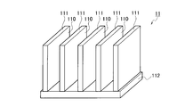
- the substrate holder 11 can employ a structure in which a cross section perpendicular to the mounting surface 110 has a comb shape, for example. That is, as shown in FIG. 2, a mounting surface 110 is defined as a main surface, a plurality of substrate mounting plates 111 that are spaced apart from each other and arranged in parallel, and a fixing plate that fixes the bottom of each of the substrate mounting plates 111.
- the substrate holder 11 having 112 can be employed.
- FIG. 2 shows an example in which the number of substrate mounting plates 111 is five, the number of substrate mounting plates 111 is not limited to five.
- the plurality of substrate mounting plates 111 are arranged alternately with the plurality of cathode electrodes 12 and the outermost side is the substrate mounting plate 111.
- a mounting surface 110 is defined on the surface of the substrate mounting plate 111 facing the cathode electrode 12.
- the substrate holder 11 with the substrate 1 mounted thereon is carried into the chamber 20. Thereafter, a process gas 100 including a film forming source gas is introduced into the chamber 20 from the gas supply device 13.
- the pressure inside the chamber 20 is adjusted by the exhaust device 15.
- a predetermined AC power is supplied between the cathode electrode 12 and the substrate holder 11 by the AC power source 14.
- the process gas 100 in the chamber 20 is turned into plasma.
- the temperature of the substrate 1 during the film forming process may be set by a substrate heater (not shown). By setting the temperature of the substrate 1 during the film formation process to a predetermined temperature, the film formation speed can be increased and the film quality can be improved.
- a desired thin film can be formed by appropriately selecting a source gas in the plasma film forming apparatus 10.
- a silicon semiconductor thin film, a silicon nitride thin film, a silicon oxide thin film, a silicon oxynitride thin film, a carbon thin film, or the like can be formed on the substrate 1.
- a silicon nitride (SiN) film is formed on the substrate 1 using a mixed gas of ammonia (NH 3 ) gas and silane (SiH 4 ) gas.
- a silicon oxide (SiO x) film is formed on the substrate 1 using a mixed gas of silane (SiH 4 ) gas and N 2 O gas.
- the cathode electrode 12 is preferably formed with a through-hole 120 that penetrates the cathode electrode 12 in the thickness direction, for example, as shown in FIG.
- the opening of the through hole 120 is formed on the surface of the cathode electrode 12 so as to face the mounting surface 110 of the substrate mounting plate 111.
- FIG. 3 exemplifies a case where there are three substrate mounting plates 111 of the substrate holder 11 and two cathode electrodes 12.
- the cathode electrode 12 provided with an opening on the surface functions as a hollow cathode electrode for generating a hollow cathode discharge.
- a hollow cathode electrode for generating a hollow cathode discharge.
- electrons emitted from the cathode electrode 12 due to ion incidence on the surface of the cathode electrode 12 are confined in the cathode electrode 12 without an electric field, thereby forming a space for high-density electrons. Gas molecules that have entered the high electron density region repeat ionization and recombination, and are observed as high-intensity emission during recombination.
- the precursor generated in the high-density plasma is a radical species, diffuses to the outside of the through-hole 120 regardless of the electrode potential, and forms a thin film on the surface of the substrate 1 disposed on the mounting surface 110 of the substrate mounting plate 111. To do.
- the cathode electrode 12A shown in FIG. 4 that employs a shower electrode structure to which the process gas 100 is supplied from the inside and that has a recess 401 formed on the surface, the recess 401 in which high-density plasma is generated by hollow cathode discharge.
- the process gas 100 is uniformly released from the gas. Thereby, plasma uniformity can be obtained over the entire surface of the cathode electrode 12A.
- the cathode electrode 12A shown in FIG. 4 it is difficult to uniformly supply the process gas 100 to a large number of the recesses 401.
- the gas ejection port 402 has a very small diameter of about 0.3 mm to 0.4 mm, it is likely to be clogged.
- hollow cathode discharge does not occur in the clogged recess 401, so that the uniformity of discharge over the entire surface of the cathode electrode 12A cannot be maintained.
- the process gas 100 is introduced without passing through the cathode electrode 12. Since the diameter of the through-hole 120 is considerably larger than the diameter of the hole required for the shower electrode, there is no fear of clogging, and maintenance is easy.
- the diameter of the through hole 120 is about 3.8 mm to 8.0 mm, for example, 5 mm.
- the plasma excited on both surfaces of the cathode electrode 12 shown in FIG. Therefore, the difference in density of the plasma concentration on both sides of the cathode electrode 12 is naturally corrected, and a plasma space having a uniform density can be generated on both sides of the cathode electrode 12.
- the multi-hollow discharge is a discharge generated on the surface of the cathode electrode 12 by combining the hollow cathode discharges generated in the respective through holes 120. Thereby, uniform high-density plasma can be realized on the surface of the cathode electrode 12. As a result, the source gas is efficiently decomposed, and a thin film is uniformly formed on the substrate 1 in a large area at a high speed.
- the through-holes 120 are preferably arranged closest to the surface of the cathode electrode 12. By arranging the through holes 120 with the highest possible density, a uniform high electron density electric field can be easily formed on both sides of the cathode electrode 12.
- FIG. 5 shows an example of the surface of the cathode electrode 12 in which the opening of the through hole 120 is formed.
- the inner surface of the through hole 120 of the cathode electrode 12 is preferably subjected to a surface treatment using a material having a good secondary electron emission rate.
- a carbon material that is inexpensive, easy to process, and easy to maintain such as cleaning is suitable for the material of the cathode electrode 12.
- the cathode electrode 12 made of a carbon material can be cleaned by hydrofluoric acid treatment.
- the use of the carbon material does not cause deformation due to high temperature in the plasma treatment process.
- an aluminum alloy or the like on which a metal oxide film is easily formed is a material suitable for the hollow cathode electrode.
- carbon containing carbon fiber, stainless alloy, copper, copper alloy, glass, ceramics, and the like can be used for the cathode electrode 12.
- the above material may be coated by alumite treatment, plating, or thermal spraying.
- a carbon material is also preferably used for the substrate holder 11 used as the anode electrode. Further, carbon containing carbon fiber, aluminum alloy, stainless alloy, copper, copper alloy, glass, ceramics, and the like can be used for the substrate holder 11. Alternatively, these materials may be coated by alumite treatment, plating, or thermal spraying.
- the process gas 100 between the substrate holder 11 and the cathode electrode 12 from below to above.
- gas molecules and radical particles having a light specific gravity that have been turned into plasma naturally flow upward on the surface of the cathode electrode 12 as an upward flow. Therefore, the process gas is uniformly supplied to the surface of the cathode electrode 12 without using a complicated structure such as a shower electrode.
- the surface of the cathode electrode 12 is so flat that the finish symbol is represented by “ ⁇ ” so that the process gas 100 flows smoothly. That is, it is preferable that the maximum height Ry is 6.3S, the ten-point average roughness Rz is 6.3Z, and the arithmetic average roughness Ra is smaller than 1.6a. By reducing the surface roughness of the cathode electrode 12, the growth rate of the thin film formed on the substrate 1 can be increased.
- the surface of the substrate holder 11 is also flat to the extent that the finish symbol is represented by “ ⁇ ”. That is, it is preferable that the maximum height Ry is 25S, the ten-point average roughness Rz is 25Z, and the arithmetic average roughness Ra is smaller than 6.3a.
- the gas supply nozzle 130 that ejects the process gas 100 of the gas supply device 13 is arranged along the bottom surface of the cathode electrode 12 as shown in FIG. It is arranged immediately below. By ejecting the process gas 100 from the gas supply nozzle 130 toward the bottom of the cathode electrode 12, the process gas 100 can be supplied almost evenly to both surfaces of the cathode electrode 12.
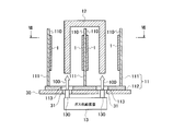
- the gas introduction holes 113 penetrating the fixing plate 112 in the vertical direction are provided between the substrate mounting plates 111 as shown in FIG. 6.
- the fixing plate 112 is formed.
- the process gas 100 is introduced between the substrate mounting plate 111 and the cathode electrode 12 from below the chamber 20 through the gas introduction hole 113.
- the support table 30 penetrates the support table 30 in the vertical direction at a position corresponding to the gas introduction hole 113 of the support table 30.
- An introduction hole 31 is formed.
- the gas supply nozzles 130 When there are a plurality of gas supply nozzles 130, the gas supply nozzles 130 are arranged along the bottom surface of the cathode electrode 12 as shown in FIG. As shown in FIG. 8 illustrating the substrate mounting plate 111 through the cathode electrode 12, the mounting surface 110 is defined on the surface of the substrate mounting plate 111 facing the cathode electrode 12. As a result, the substrate 1 is disposed to face the cathode electrode 12.
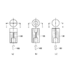
- FIG. 9A to 9C show examples of the shape of the ejection port of the gas supply nozzle 130.
- FIG. 9A shows an example in which a groove is formed along the diameter at the tip of the cylindrical gas supply nozzle 130 and an ejection port is arranged at the center of the groove.
- FIG. 9B shows an example in which a concave portion is provided at the tip of the cylindrical gas supply nozzle 130 and an ejection port is arranged at the central portion of the bottom surface of the concave portion.
- FIG. 9C is an example in which an ejection port is arranged at the center of the tip of the cylindrical gas supply nozzle 130.
- the process gas 100 is a gas in which a plurality of types of gases are mixed
- the process gas 100 in which all the gases are mixed may be supplied from the gas supply nozzle 130, or the gas supply nozzle 130 that is different for each type of gas.
- the gas may be supplied from each.
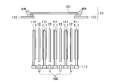
- FIG. 10 shows a configuration example of the exhaust device 15.
- the exhaust device 15 shown in FIG. 10 is disposed on the upper portion of the chamber 20 (not shown).
- the exhaust device 15 has a first exhaust adjustment plate 151 disposed above the substrate holder 11 and the cathode electrode 12 and a frame shape disposed so as to be positioned below the outer edge of the first exhaust adjustment plate 151.
- a second exhaust adjustment plate 152 As shown in FIG. 10, the process gas 100 that has flowed above the substrate holder 11 and the cathode electrode 12 passes through the gap between the first exhaust adjustment plate 151 and the second exhaust adjustment plate 152, and the first gas The gas is discharged from the outer edge of the exhaust adjustment plate 151 to the outside of the chamber 20.
- the exhaust device 15 adjusts the exhaust amount by controlling the width of the gap between the first exhaust adjustment plate 151 and the second exhaust adjustment plate 152.
- FIG. 11 shows another configuration example of the exhaust device 15.
- the exhaust device 15 shown in FIG. 11 is disposed on the upper portion of the chamber 20 (not shown) and has a large number of exhaust holes 150 penetrating in the vertical direction.
- the process gas 100 is exhausted to the outside of the chamber 20 through the exhaust hole 150.
- the exhaust device 15 adjusts the exhaust amount by controlling the opening degree of the exhaust hole 150.
- the substrate 1 can be placed in the chamber 20 with the film forming surface of the substrate 1 vertical by using the substrate holder 11 as an anode electrode. For this reason, a plurality of cathode electrodes 12 are arranged in the chamber 20. Therefore, the plasma film forming apparatus 10 shown in FIG. 1 has a larger number of substrates 1 than the plasma film forming apparatus in which the film forming surface is mounted on a flat substrate plate or the like and the film forming process is performed. Can be stored in the chamber 20 at the same time, and the processing capability can be remarkably improved.
- the cathode electrode 12 in which the through-hole 120 is formed uniform and high-density plasma can be stably generated on both surfaces of the cathode electrode 12.
- uniform high-density plasma can be generated in a large area regardless of the frequency of the AC power supplied from the AC power supply 14.
- the frequency of the AC power supplied by the AC power supply 14 is set to, for example, about 60 Hz to 27 MHz, uniform and high-density plasma can be generated. That is, there is no need to use an AC power supply that supplies expensive VHF band AC power.
- the plasma film forming apparatus 10 can obtain a high-density plasma equivalent to or higher than that of a conventional plasma film forming apparatus using a VHF band AC power source even in a low frequency RF band such as 250 KHz.
- a large-area thin film can be formed on the substrate 1 uniformly at a high speed. That is, according to the plasma film forming apparatus 10, the film thickness and the film quality uniformity of the formed film are improved, and the film forming speed is improved.
- the plasma film forming apparatus 10 it is not necessary to use a shower electrode that has a complicated structure and needs to form fine holes. For this reason, the frequent maintenance like a shower electrode is unnecessary. Furthermore, the shower electrode needs to be enlarged in order to disperse the process gas 100 uniformly, whereas the plasma film forming apparatus 10 does not need to be enlarged. Therefore, according to the plasma film forming apparatus 10, it is possible to provide a plasma film forming apparatus that can efficiently form a uniform film on all the substrates in the chamber 20 and that is suppressed in size.
- the manufacturing period of the plasma film forming apparatus 10 is shorter and the manufacturing yield is improved as compared with a plasma film forming apparatus using a shower electrode that requires processing of several thousand or more micro holes. For this reason, the manufacturing cost of the plasma film-forming apparatus 10 is suppressed.
- FIG. 12 shows an example in which AC power output from the AC power source 14 is supplied between the substrate holder 11 and the cathode electrode 12 via the pulse generator 16.
- the output of the pulse generator 16 is supplied to the cathode electrode 12, and the substrate holder 11 is grounded.
- plasma is stably formed in the chamber 20. This is because by providing a stop period for the supply of AC power, the temperature of the electrons is lowered and the stability of the discharge is improved.
- the AC power is supplied between the substrate holder 11 and the cathode electrode 12 so that the ON time and the OFF time are alternately repeated with the ON time for supplying AC power being 600 ⁇ sec and the OFF time for stopping the supply of AC power being 50 ⁇ sec.
- the on-time is preferably set in the range of about 100 ⁇ s to 1000 ⁇ s
- the off-time is preferably set in the range of about 10 ⁇ s to 100 ⁇ s.
- the supply of AC power between the substrate holder 11 and the cathode electrode 12 is pulse-controlled to periodically turn on / off the supply of AC power, thereby suppressing the occurrence of abnormal discharge.
- FIG. 13 shows an example in which the AC power supply 17 is mounted on the substrate holder 11 which is an anode electrode, in addition to the AC power supply 14 mounted on the cathode electrode 12.
- the frequency of the AC power supplied from the AC power supply 17 may be equal to or lower than the frequency of the AC power supplied from the AC power supply 14.
- the frequency of the AC power supplied from the AC power supply 17 is set to about 60 Hz to 27 MHz.
- plasma cleaning of the substrate 1 can be performed by supplying AC power only from the AC power supply 17 without supplying AC power from the AC power supply 14.
- a sputtering gas is introduced into the chamber 20, and the substrate 1 is cleaned by sputter etching while supplying AC power from the AC power supply 17.
- the output of the AC power supply 14 may be divided by a power splitter 18, and the divided AC power may be supplied to the cathode electrode 12 and the substrate holder 11, respectively.
- the power supplied to the substrate holder 11 may be smaller than the power supplied to the cathode electrode 12. For example, 90% to 100% AC power is supplied to the cathode electrode 12 and 10% to 0% AC power is supplied to the substrate holder 11.
- the plasma film forming apparatus 10 shown in FIG. 1 can be used, for example, as a film forming chamber of an in-line type film forming apparatus.
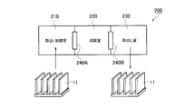
- FIG. 15 shows an example of an in-line film forming apparatus 200 including three chambers: a take-in / heat chamber 210, a film forming chamber 220, and a take-out chamber 230.
- the substrate holder 11 on which the substrate 1 is mounted is taken into the take-in / heating chamber 210.
- the substrate holder 11 is transferred from the take-in / heat chamber 210 to the film formation chamber 220 through the open / close gate 240 ⁇ / b> A.
- the substrate holder 11 is transferred from the film formation chamber 220 to the take-out chamber 230 through the openable gate 240 ⁇ / b> B.
- the substrate holder 11 is taken out from the take-out chamber 230.
- the substrate holder 11 is transferred between the chambers of the inline-type film forming apparatus 200 by a transfer device (not shown).
- the chamber 20 is preferably cylindrical. By making it cylindrical shape, the chamber 20 can have sufficient strength as a vacuum vessel. For this reason, even if the thickness of the chamber 20 is reduced, sufficient strength can be realized with an inexpensive and simple structure including during heating.
- FIG. 17 shows a configuration example of the intake / heating chamber 210.
- the take-in / heating chamber 210 includes heaters 211 ⁇ / b> A disposed above and below the substrate holder 11 and slot heaters 211 ⁇ / b> B disposed between the substrate mounting plates 111 in parallel with the substrate mounting plate 111.
- the substrate holder 11 is supported in the take-in / heating chamber 210 by a support table 212.
- a heat insulating plate 213 is disposed between the support base 212 and the slot heater 211B.
- the slot heater 211 ⁇ / b> B heats the substrate 1 mounted on the substrate holder 11 and the mounting surface 110, thereby preventing a temperature difference between the substrate 1 and the substrate holder 11. For example, when preheating is performed while monitoring the temperature of the substrate holder 11, the temperature of the substrate 1 can be accurately adjusted.
- a lamp heater As the heater 211A and the slot heater 211B, a lamp heater, a ceramic heater, a sheathed heater, an induction heater, or the like can be employed.
- the plasma film forming apparatus 10 shown in FIG. 1 is applied to the in-line type film forming apparatus 200 having two rooms as shown in FIG. May be.
- the substrate holder 11 is taken in and out of the heating chamber 211. After the substrate 1 taken into the heating chamber 211 is preheated to a predetermined temperature in the heating chamber 211, the substrate holder 11 is transferred to the film formation chamber 220 through the openable gate 241. After a thin film is formed on the substrate 1 in the film formation chamber 220, the substrate holder 11 is transferred to the heating chamber 211 through the gate 241.
- the substrate holder 11 is taken out from the heating chamber 211.
- the slot heater 211 ⁇ / b> B between the substrate mounting plates 111 in the heating chamber 211 shown in FIG. 18.
- the shape of the substrate holder 11 is not limited thereto.
- the substrate holder 11 may be a single plate.
- the plasma film forming apparatus of the present invention can be used in the manufacturing industry of semiconductor devices that form a film on a substrate.
Landscapes
- Chemical & Material Sciences (AREA)
- Engineering & Computer Science (AREA)
- Physics & Mathematics (AREA)
- Plasma & Fusion (AREA)
- Organic Chemistry (AREA)
- General Chemical & Material Sciences (AREA)
- Chemical Kinetics & Catalysis (AREA)
- Materials Engineering (AREA)
- Mechanical Engineering (AREA)
- Metallurgy (AREA)
- Analytical Chemistry (AREA)
- Spectroscopy & Molecular Physics (AREA)
- Electromagnetism (AREA)
- Power Engineering (AREA)
- Chemical Vapour Deposition (AREA)
- Plasma Technology (AREA)
Abstract
Description
Claims (12)
- 基板が搭載される搭載面を有する基板ホルダーが搬入されるチャンバーと、
前記チャンバー内で上下方向に延伸して配置される前記搭載面と対向するように配置されたカソード電極と、
前記チャンバー内の前記基板ホルダーと前記カソード電極間にプロセスガスを導入するガス供給装置と、
前記基板ホルダーと前記カソード電極間に交流電力を供給して、基板ホルダーと前記カソード電極間において前記プロセスガスをプラズマ状態にする交流電源と
を備え、前記プロセスガスに含まれる原料を主成分とする薄膜を前記基板上に形成することを特徴とするプラズマ成膜装置。 - 前記ガス供給装置が、下方から上方に向かって前記チャンバー内にプロセスガスを導入することを特徴とする請求項1に記載のプラズマ成膜装置。
- 前記ガス供給装置が、前記カソード電極の底面に沿って配置されたガス供給ノズルから前記カソード電極の底部に向けて前記プロセスガスを噴き出すことを特徴とする請求項2に記載のプラズマ成膜装置。
- 前記基板ホルダーが、前記搭載面が主面にそれぞれ定義され、互いに離間し且つ平行に配置された複数の基板取り付け板を有することを特徴とする請求項1に記載のプラズマ成膜装置。
- 前記複数の基板取り付け板が、前記複数のカソード電極と交互に、且つ最外側が前記基板取り付け板であるように配列され、前記基板取り付け板の前記カソード電極に対向する面に前記搭載面がそれぞれ定義されていることを特徴とする請求項4に記載のプラズマ成膜装置。
- 前記基板ホルダーが、
前記複数の基板取り付け板のそれぞれの底部を固定し、上下方向に貫通するガス導入孔が前記複数の基板取り付け板間に形成された固定板を有し、
前記ガス導入孔を介して前記基板取り付け板と前記カソード電極間に前記プロセスガスが導入されることを特徴とする請求項4に記載のプラズマ成膜装置。 - 前記カソード電極が、前記搭載面に対向する面に開口部が設けられた貫通孔を有することを特徴とする請求項1に記載のプラズマ成膜装置。
- 前記チャンバーが円筒形状であることを特徴とする請求項1に記載のプラズマ成膜装置。
- 前記薄膜を前記基板上に形成する前に前記基板ホルダーが格納される加熱室を更に備え、前記加熱室が、
前記複数の基板取り付け板の間に配置されて、前記基板ホルダー及び前記搭載面に搭載された前記基板を加熱するスロットヒータ
を備えることを特徴とする請求項4に記載のプラズマ成膜装置。 - 前記基板ホルダー及び前記カソード電極の少なくともいずれかがカーボンからなることを特徴とする請求項1に記載のプラズマ成膜装置。
- 前記カソード電極の表面粗さについて最大高さが6.3S以下であることを特徴とする請求項1に記載のプラズマ成膜装置。
- 前記基板ホルダーの表面粗さにおける最大高さが25S以下であることを特徴とする請求項1に記載のプラズマ成膜装置。
Priority Applications (5)
| Application Number | Priority Date | Filing Date | Title |
|---|---|---|---|
| KR1020147001147A KR101650795B1 (ko) | 2011-09-26 | 2011-09-26 | 플라즈마 성막 장치 |
| PCT/JP2011/071796 WO2013046286A1 (ja) | 2011-09-26 | 2011-09-26 | プラズマ成膜装置 |
| JP2013535647A JP5768890B2 (ja) | 2011-09-26 | 2011-09-26 | プラズマ成膜装置 |
| CN201180072547.7A CN103890229B (zh) | 2011-09-26 | 2011-09-26 | 等离子体成膜装置 |
| TW101135387A TWI494466B (zh) | 2011-09-26 | 2012-09-26 | 電漿成膜裝置、結晶太陽電池與半導體元件 |
Applications Claiming Priority (1)
| Application Number | Priority Date | Filing Date | Title |
|---|---|---|---|
| PCT/JP2011/071796 WO2013046286A1 (ja) | 2011-09-26 | 2011-09-26 | プラズマ成膜装置 |
Publications (1)
| Publication Number | Publication Date |
|---|---|
| WO2013046286A1 true WO2013046286A1 (ja) | 2013-04-04 |
Family
ID=47994406
Family Applications (1)
| Application Number | Title | Priority Date | Filing Date |
|---|---|---|---|
| PCT/JP2011/071796 Ceased WO2013046286A1 (ja) | 2011-09-26 | 2011-09-26 | プラズマ成膜装置 |
Country Status (5)
| Country | Link |
|---|---|
| JP (1) | JP5768890B2 (ja) |
| KR (1) | KR101650795B1 (ja) |
| CN (1) | CN103890229B (ja) |
| TW (1) | TWI494466B (ja) |
| WO (1) | WO2013046286A1 (ja) |
Cited By (7)
| Publication number | Priority date | Publication date | Assignee | Title |
|---|---|---|---|---|
| WO2014188576A1 (ja) * | 2013-05-24 | 2014-11-27 | 株式会社島津製作所 | プラズマ処理装置 |
| JP2015015382A (ja) * | 2013-07-05 | 2015-01-22 | 株式会社島津製作所 | 成膜装置及び成膜方法 |
| WO2017005253A1 (de) * | 2015-07-09 | 2017-01-12 | Hanwha Q Cells Gmbh | Vorrichtung zur paarweisen aufnahme von substraten |
| WO2018016131A1 (ja) * | 2016-07-21 | 2018-01-25 | 株式会社日立国際電気 | プラズマ生成装置、基板処理装置及び半導体装置の製造方法 |
| EP3367419A1 (de) * | 2017-02-28 | 2018-08-29 | Meyer Burger (Germany) AG | Elektrodeneinheit mit einem internen elektrischen netzwerk zur zuführung von hochfrequenter spannung und trägeranordnung für eine plasmabehandlungsanlage |
| EP3751018A4 (en) * | 2018-02-06 | 2021-10-13 | Jiangsu Leadmicro Nano-Technology Co., Ltd. | VACUUM REACTION DEVICE AND REACTION METHOD |
| DE102020112641A1 (de) | 2020-05-11 | 2021-11-11 | Hanwha Q Cells Gmbh | Haltevorrichtung und Verwendung der Haltevorrichtung |
Families Citing this family (2)
| Publication number | Priority date | Publication date | Assignee | Title |
|---|---|---|---|---|
| MX2022003626A (es) | 2019-09-25 | 2022-05-03 | Shibaura Machine Co Ltd | Dispositivo de tratamiento de superficie. |
| CN111893455B (zh) * | 2020-09-08 | 2023-10-03 | 河北美普兰地环保科技有限公司 | 金属基材碳纳米膜材料制造设备及其制备方法 |
Citations (4)
| Publication number | Priority date | Publication date | Assignee | Title |
|---|---|---|---|---|
| JPH05209279A (ja) * | 1991-10-29 | 1993-08-20 | Canon Inc | 金属膜形成装置および金属膜形成法 |
| JP2001192835A (ja) * | 2000-01-11 | 2001-07-17 | Kanegafuchi Chem Ind Co Ltd | インライン型プラズマcvd装置において用いられる基板搬送カート |
| JP2007227436A (ja) * | 2006-02-21 | 2007-09-06 | Ishikawajima Harima Heavy Ind Co Ltd | 真空成膜装置 |
| JP2009231385A (ja) * | 2008-03-19 | 2009-10-08 | Sanyo Electric Co Ltd | 半導体装置の製造方法 |
Family Cites Families (4)
| Publication number | Priority date | Publication date | Assignee | Title |
|---|---|---|---|---|
| JP3586197B2 (ja) * | 2000-03-23 | 2004-11-10 | シャープ株式会社 | 薄膜形成用プラズマ成膜装置 |
| WO2002020871A1 (de) | 2000-09-08 | 2002-03-14 | Centrotherm Elektrische Anlagen Gmbh + Co. | Plasmaboot |
| JP2009164515A (ja) * | 2008-01-10 | 2009-07-23 | Shimadzu Corp | 反射防止膜成膜方法および太陽電池 |
| JP2011077323A (ja) * | 2009-09-30 | 2011-04-14 | Tokyo Electron Ltd | 窒化珪素膜の成膜方法および半導体メモリ装置の製造方法 |
-
2011
- 2011-09-26 WO PCT/JP2011/071796 patent/WO2013046286A1/ja not_active Ceased
- 2011-09-26 KR KR1020147001147A patent/KR101650795B1/ko not_active Expired - Fee Related
- 2011-09-26 CN CN201180072547.7A patent/CN103890229B/zh not_active Expired - Fee Related
- 2011-09-26 JP JP2013535647A patent/JP5768890B2/ja not_active Expired - Fee Related
-
2012
- 2012-09-26 TW TW101135387A patent/TWI494466B/zh not_active IP Right Cessation
Patent Citations (4)
| Publication number | Priority date | Publication date | Assignee | Title |
|---|---|---|---|---|
| JPH05209279A (ja) * | 1991-10-29 | 1993-08-20 | Canon Inc | 金属膜形成装置および金属膜形成法 |
| JP2001192835A (ja) * | 2000-01-11 | 2001-07-17 | Kanegafuchi Chem Ind Co Ltd | インライン型プラズマcvd装置において用いられる基板搬送カート |
| JP2007227436A (ja) * | 2006-02-21 | 2007-09-06 | Ishikawajima Harima Heavy Ind Co Ltd | 真空成膜装置 |
| JP2009231385A (ja) * | 2008-03-19 | 2009-10-08 | Sanyo Electric Co Ltd | 半導体装置の製造方法 |
Cited By (12)
| Publication number | Priority date | Publication date | Assignee | Title |
|---|---|---|---|---|
| WO2014188576A1 (ja) * | 2013-05-24 | 2014-11-27 | 株式会社島津製作所 | プラズマ処理装置 |
| JP6065111B2 (ja) * | 2013-05-24 | 2017-01-25 | 株式会社島津製作所 | プラズマ処理装置 |
| JP2015015382A (ja) * | 2013-07-05 | 2015-01-22 | 株式会社島津製作所 | 成膜装置及び成膜方法 |
| WO2017005253A1 (de) * | 2015-07-09 | 2017-01-12 | Hanwha Q Cells Gmbh | Vorrichtung zur paarweisen aufnahme von substraten |
| WO2018016131A1 (ja) * | 2016-07-21 | 2018-01-25 | 株式会社日立国際電気 | プラズマ生成装置、基板処理装置及び半導体装置の製造方法 |
| JPWO2018016131A1 (ja) * | 2016-07-21 | 2019-01-31 | 株式会社Kokusai Electric | プラズマ生成装置、基板処理装置、半導体装置の製造方法及びプログラム |
| EP3367419A1 (de) * | 2017-02-28 | 2018-08-29 | Meyer Burger (Germany) AG | Elektrodeneinheit mit einem internen elektrischen netzwerk zur zuführung von hochfrequenter spannung und trägeranordnung für eine plasmabehandlungsanlage |
| WO2018158013A1 (de) * | 2017-02-28 | 2018-09-07 | Meyer Burger (Germany) Ag | Elektrodeneinheit mit einem internen elektrischen netzwerk zur zuführung von hochfrequenter spannung und trägeranordnung für eine plasmabehandlungsanlage |
| KR20190114015A (ko) * | 2017-02-28 | 2019-10-08 | 마이어 버거 (저머니) 게엠베하 | 고주파수 전압을 공급하기 위한 내부 전기 네트워크를 갖는 전자 유닛 및 플라즈마 처리 시스템을 위한 캐리어 어레인지먼트 |
| KR102124434B1 (ko) | 2017-02-28 | 2020-06-18 | 마이어 버거 (저머니) 게엠베하 | 고주파수 전압을 공급하기 위한 내부 전기 네트워크를 갖는 전자 유닛 및 플라즈마 처리 시스템을 위한 캐리어 어레인지먼트 |
| EP3751018A4 (en) * | 2018-02-06 | 2021-10-13 | Jiangsu Leadmicro Nano-Technology Co., Ltd. | VACUUM REACTION DEVICE AND REACTION METHOD |
| DE102020112641A1 (de) | 2020-05-11 | 2021-11-11 | Hanwha Q Cells Gmbh | Haltevorrichtung und Verwendung der Haltevorrichtung |
Also Published As
| Publication number | Publication date |
|---|---|
| TWI494466B (zh) | 2015-08-01 |
| JP5768890B2 (ja) | 2015-08-26 |
| CN103890229B (zh) | 2015-12-16 |
| KR20140037226A (ko) | 2014-03-26 |
| TW201321550A (zh) | 2013-06-01 |
| CN103890229A (zh) | 2014-06-25 |
| KR101650795B1 (ko) | 2016-08-24 |
| JPWO2013046286A1 (ja) | 2015-03-26 |
Similar Documents
| Publication | Publication Date | Title |
|---|---|---|
| JP5768890B2 (ja) | プラズマ成膜装置 | |
| CN103493602B (zh) | 等离子体处理装置 | |
| CN102017057B (zh) | 用于基板的等离子体辅助处理的等离子体处理装置和方法 | |
| JP6386519B2 (ja) | Cvd装置、及び、cvd膜の製造方法 | |
| CN101971292B (zh) | 等离子体cvd用阴电极和等离子体cvd装置 | |
| KR101696333B1 (ko) | 감소된 공구 풋 프린트를 갖는, 균일한 박막 증착을 위한 평행판 반응기 | |
| CN1323751C (zh) | 等离子体处理装置、生成等离子体反应容器的制造方法及等离子体处理方法 | |
| CN1316095A (zh) | 改进的固定均匀环设计 | |
| TW200816278A (en) | Shower plate, plasma processing device using the same, plasma processing method and manufacturing method of electronic apparatus | |
| US20110042008A1 (en) | Plasma generator | |
| US7927455B2 (en) | Plasma processing apparatus | |
| WO2012160718A1 (ja) | 薄膜形成装置 | |
| TWI744378B (zh) | 工件處理裝置 | |
| CN108779555A (zh) | 设备和方法 | |
| JP2004353066A (ja) | プラズマ源およびプラズマ処理装置 | |
| US20220270860A1 (en) | Spatially controlled plasma | |
| JP2010218801A (ja) | 大気圧プラズマ発生装置 | |
| US6350961B1 (en) | Method and device for improving surfaces | |
| KR102224586B1 (ko) | 처리 챔버들을 위한 코팅 재료 | |
| JP2017054943A (ja) | プラズマ処理装置 | |
| WO2014188576A1 (ja) | プラズマ処理装置 | |
| JP2000034571A (ja) | 表面処理装置 |
Legal Events
| Date | Code | Title | Description |
|---|---|---|---|
| 121 | Ep: the epo has been informed by wipo that ep was designated in this application |
Ref document number: 11872903 Country of ref document: EP Kind code of ref document: A1 |
|
| ENP | Entry into the national phase |
Ref document number: 2013535647 Country of ref document: JP Kind code of ref document: A |
|
| ENP | Entry into the national phase |
Ref document number: 20147001147 Country of ref document: KR Kind code of ref document: A |
|
| NENP | Non-entry into the national phase |
Ref country code: DE |
|
| 122 | Ep: pct application non-entry in european phase |
Ref document number: 11872903 Country of ref document: EP Kind code of ref document: A1 |