WO2013069728A1 - ショットキーバリアダイオード - Google Patents
ショットキーバリアダイオード Download PDFInfo
- Publication number
- WO2013069728A1 WO2013069728A1 PCT/JP2012/078983 JP2012078983W WO2013069728A1 WO 2013069728 A1 WO2013069728 A1 WO 2013069728A1 JP 2012078983 W JP2012078983 W JP 2012078983W WO 2013069728 A1 WO2013069728 A1 WO 2013069728A1
- Authority
- WO
- WIPO (PCT)
- Prior art keywords
- semiconductor layer
- schottky
- layer
- carrier concentration
- electron carrier
- Prior art date
- Legal status (The legal status is an assumption and is not a legal conclusion. Google has not performed a legal analysis and makes no representation as to the accuracy of the status listed.)
- Ceased
Links
Images





Classifications
-
- H—ELECTRICITY
- H10—SEMICONDUCTOR DEVICES; ELECTRIC SOLID-STATE DEVICES NOT OTHERWISE PROVIDED FOR
- H10D—INORGANIC ELECTRIC SEMICONDUCTOR DEVICES
- H10D8/00—Diodes
- H10D8/60—Schottky-barrier diodes
-
- H—ELECTRICITY
- H10—SEMICONDUCTOR DEVICES; ELECTRIC SOLID-STATE DEVICES NOT OTHERWISE PROVIDED FOR
- H10D—INORGANIC ELECTRIC SEMICONDUCTOR DEVICES
- H10D62/00—Semiconductor bodies, or regions thereof, of devices having potential barriers
- H10D62/10—Shapes, relative sizes or dispositions of the regions of the semiconductor bodies; Shapes of the semiconductor bodies
- H10D62/102—Constructional design considerations for preventing surface leakage or controlling electric field concentration
- H10D62/103—Constructional design considerations for preventing surface leakage or controlling electric field concentration for increasing or controlling the breakdown voltage of reverse-biased devices
- H10D62/104—Constructional design considerations for preventing surface leakage or controlling electric field concentration for increasing or controlling the breakdown voltage of reverse-biased devices having particular shapes of the bodies at or near reverse-biased junctions, e.g. having bevels or moats
-
- H—ELECTRICITY
- H10—SEMICONDUCTOR DEVICES; ELECTRIC SOLID-STATE DEVICES NOT OTHERWISE PROVIDED FOR
- H10D—INORGANIC ELECTRIC SEMICONDUCTOR DEVICES
- H10D62/00—Semiconductor bodies, or regions thereof, of devices having potential barriers
- H10D62/10—Shapes, relative sizes or dispositions of the regions of the semiconductor bodies; Shapes of the semiconductor bodies
- H10D62/102—Constructional design considerations for preventing surface leakage or controlling electric field concentration
- H10D62/103—Constructional design considerations for preventing surface leakage or controlling electric field concentration for increasing or controlling the breakdown voltage of reverse-biased devices
- H10D62/105—Constructional design considerations for preventing surface leakage or controlling electric field concentration for increasing or controlling the breakdown voltage of reverse-biased devices by having particular doping profiles, shapes or arrangements of PN junctions; by having supplementary regions, e.g. junction termination extension [JTE]
- H10D62/106—Constructional design considerations for preventing surface leakage or controlling electric field concentration for increasing or controlling the breakdown voltage of reverse-biased devices by having particular doping profiles, shapes or arrangements of PN junctions; by having supplementary regions, e.g. junction termination extension [JTE] having supplementary regions doped oppositely to or in rectifying contact with regions of the semiconductor bodies, e.g. guard rings with PN or Schottky junctions
-
- H—ELECTRICITY
- H10—SEMICONDUCTOR DEVICES; ELECTRIC SOLID-STATE DEVICES NOT OTHERWISE PROVIDED FOR
- H10D—INORGANIC ELECTRIC SEMICONDUCTOR DEVICES
- H10D62/00—Semiconductor bodies, or regions thereof, of devices having potential barriers
- H10D62/40—Crystalline structures
- H10D62/405—Orientations of crystalline planes
-
- H—ELECTRICITY
- H10—SEMICONDUCTOR DEVICES; ELECTRIC SOLID-STATE DEVICES NOT OTHERWISE PROVIDED FOR
- H10D—INORGANIC ELECTRIC SEMICONDUCTOR DEVICES
- H10D62/00—Semiconductor bodies, or regions thereof, of devices having potential barriers
- H10D62/80—Semiconductor bodies, or regions thereof, of devices having potential barriers characterised by the materials
-
- H—ELECTRICITY
- H10—SEMICONDUCTOR DEVICES; ELECTRIC SOLID-STATE DEVICES NOT OTHERWISE PROVIDED FOR
- H10D—INORGANIC ELECTRIC SEMICONDUCTOR DEVICES
- H10D62/00—Semiconductor bodies, or regions thereof, of devices having potential barriers
- H10D62/80—Semiconductor bodies, or regions thereof, of devices having potential barriers characterised by the materials
- H10D62/82—Heterojunctions
-
- H—ELECTRICITY
- H10—SEMICONDUCTOR DEVICES; ELECTRIC SOLID-STATE DEVICES NOT OTHERWISE PROVIDED FOR
- H10D—INORGANIC ELECTRIC SEMICONDUCTOR DEVICES
- H10D62/00—Semiconductor bodies, or regions thereof, of devices having potential barriers
- H10D62/80—Semiconductor bodies, or regions thereof, of devices having potential barriers characterised by the materials
- H10D62/875—Semiconductor bodies, or regions thereof, of devices having potential barriers characterised by the materials being semiconductor metal oxide, e.g. InGaZnO
-
- H—ELECTRICITY
- H10—SEMICONDUCTOR DEVICES; ELECTRIC SOLID-STATE DEVICES NOT OTHERWISE PROVIDED FOR
- H10D—INORGANIC ELECTRIC SEMICONDUCTOR DEVICES
- H10D64/00—Electrodes of devices having potential barriers
- H10D64/60—Electrodes characterised by their materials
- H10D64/64—Electrodes comprising a Schottky barrier to a semiconductor
-
- H—ELECTRICITY
- H10—SEMICONDUCTOR DEVICES; ELECTRIC SOLID-STATE DEVICES NOT OTHERWISE PROVIDED FOR
- H10D—INORGANIC ELECTRIC SEMICONDUCTOR DEVICES
- H10D99/00—Subject matter not provided for in other groups of this subclass
-
- H—ELECTRICITY
- H10—SEMICONDUCTOR DEVICES; ELECTRIC SOLID-STATE DEVICES NOT OTHERWISE PROVIDED FOR
- H10P—GENERIC PROCESSES OR APPARATUS FOR THE MANUFACTURE OR TREATMENT OF DEVICES COVERED BY CLASS H10
- H10P14/00—Formation of materials, e.g. in the shape of layers or pillars
- H10P14/20—Formation of materials, e.g. in the shape of layers or pillars of semiconductor materials
- H10P14/22—Formation of materials, e.g. in the shape of layers or pillars of semiconductor materials using physical deposition, e.g. vacuum deposition or sputtering
-
- H—ELECTRICITY
- H10—SEMICONDUCTOR DEVICES; ELECTRIC SOLID-STATE DEVICES NOT OTHERWISE PROVIDED FOR
- H10P—GENERIC PROCESSES OR APPARATUS FOR THE MANUFACTURE OR TREATMENT OF DEVICES COVERED BY CLASS H10
- H10P14/00—Formation of materials, e.g. in the shape of layers or pillars
- H10P14/20—Formation of materials, e.g. in the shape of layers or pillars of semiconductor materials
- H10P14/29—Formation of materials, e.g. in the shape of layers or pillars of semiconductor materials characterised by the substrates
- H10P14/2901—Materials
- H10P14/2918—Materials being semiconductor metal oxides
-
- H—ELECTRICITY
- H10—SEMICONDUCTOR DEVICES; ELECTRIC SOLID-STATE DEVICES NOT OTHERWISE PROVIDED FOR
- H10P—GENERIC PROCESSES OR APPARATUS FOR THE MANUFACTURE OR TREATMENT OF DEVICES COVERED BY CLASS H10
- H10P14/00—Formation of materials, e.g. in the shape of layers or pillars
- H10P14/20—Formation of materials, e.g. in the shape of layers or pillars of semiconductor materials
- H10P14/29—Formation of materials, e.g. in the shape of layers or pillars of semiconductor materials characterised by the substrates
- H10P14/2926—Crystal orientations
-
- H—ELECTRICITY
- H10—SEMICONDUCTOR DEVICES; ELECTRIC SOLID-STATE DEVICES NOT OTHERWISE PROVIDED FOR
- H10P—GENERIC PROCESSES OR APPARATUS FOR THE MANUFACTURE OR TREATMENT OF DEVICES COVERED BY CLASS H10
- H10P14/00—Formation of materials, e.g. in the shape of layers or pillars
- H10P14/20—Formation of materials, e.g. in the shape of layers or pillars of semiconductor materials
- H10P14/34—Deposited materials, e.g. layers
- H10P14/3402—Deposited materials, e.g. layers characterised by the chemical composition
- H10P14/3434—Deposited materials, e.g. layers characterised by the chemical composition being oxide semiconductor materials
-
- H—ELECTRICITY
- H10—SEMICONDUCTOR DEVICES; ELECTRIC SOLID-STATE DEVICES NOT OTHERWISE PROVIDED FOR
- H10P—GENERIC PROCESSES OR APPARATUS FOR THE MANUFACTURE OR TREATMENT OF DEVICES COVERED BY CLASS H10
- H10P14/00—Formation of materials, e.g. in the shape of layers or pillars
- H10P14/20—Formation of materials, e.g. in the shape of layers or pillars of semiconductor materials
- H10P14/34—Deposited materials, e.g. layers
- H10P14/3438—Doping during depositing
- H10P14/3441—Conductivity type
- H10P14/3442—N-type
Definitions
- the present invention relates to a Schottky barrier diode formed by bringing a metal and a semiconductor into Schottky contact.
- a Schottky barrier diode using SiC is known as a high voltage diode used in, for example, an inverter circuit (see, for example, Patent Document 1).
- a Schottky barrier diode generally has a small forward voltage (VF) and a short reverse recovery time (trr) and is excellent in switching characteristics as compared with a PN junction diode having a comparable current capacity.
- VF forward voltage
- trr reverse recovery time
- VF forward voltage
- VRM reverse breakdown voltage
- an object of the present invention is to provide a Schottky barrier diode capable of suppressing an increase in forward voltage and an increase in contact resistance with an ohmic electrode layer even if the reverse breakdown voltage is increased.
- the present invention provides the following Schottky barrier diodes described in [1] to [4].
- An n-type semiconductor layer made of a Ga 2 O 3 -based compound semiconductor having n-type conductivity and an electrode layer in Schottky contact with the n-type semiconductor layer, A Schottky barrier diode in which a first semiconductor layer that is in Schottky contact with the electrode layer and a second semiconductor layer having a higher electron carrier concentration than the first semiconductor layer are formed.
- a Schottky barrier diode capable of suppressing an increase in forward voltage and an increase in contact resistance with an ohmic electrode layer even if the reverse breakdown voltage is increased.
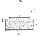
- FIG. 1 is a cross-sectional view showing a configuration example of a Schottky diode according to an embodiment of the present invention.
- FIG. 2A shows the case where Si is used as the semiconductor material and Ga 2 O 3 is used, and when the reverse breakdown voltage is set to 100 V, the electron carrier concentration, resistivity, and thickness of the n ⁇ semiconductor layer and n + semiconductor. It is a comparison table which shows the relationship between voltage drop.
- FIG. 2B shows the case where SiC is used as the semiconductor material and Ga 2 O 3 is used, and when the reverse breakdown voltage is set to 600 V, the electron carrier concentration, resistivity, and thickness of the n ⁇ semiconductor layer and n + semiconductor. It is a comparison table which shows the relationship between voltage drop.
- FIG. 2A shows the case where Si is used as the semiconductor material and Ga 2 O 3 is used, and when the reverse breakdown voltage is set to 100 V, the electron carrier concentration, resistivity, and thickness of the n ⁇ semiconductor layer and n + semiconductor. It is a comparison table which
- FIG. 2C shows the case where SiC is used as the semiconductor material and Ga 2 O 3 is used, and when the reverse breakdown voltage is set to 1000 V, the electron carrier concentration, resistivity and thickness of the n ⁇ semiconductor layer and n + semiconductor. It is a comparison table which shows the relationship between voltage drop.
- FIG. 2D shows the case where SiC is used as the semiconductor material and Ga 2 O 3 is used, and when the reverse breakdown voltage is set to 10000 V, the electron carrier concentration, resistivity and thickness of the n ⁇ semiconductor layer and n + semiconductor. It is a comparison table which shows the relationship between voltage drop.
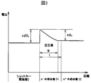
- FIG. 3 is a schematic view illustrating an energy band in the Schottky diode according to the embodiment of the invention.
- FIG. 3 is a schematic view illustrating an energy band in the Schottky diode according to the embodiment of the invention.
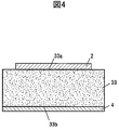
- FIG. 4 is a cross-sectional view illustrating a configuration example of a Schottky diode according to a comparative example.
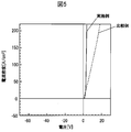
- FIG. 5 is a graph showing voltage-current density characteristics of the Schottky diode according to the example and the Schottky diode according to the comparative example.
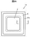
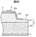
- FIG. 6A is a plan view showing a Schottky diode according to a first modification of the embodiment of the present invention. 6B is a cross-sectional view taken along the line AA in FIG. 6A.
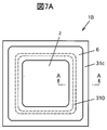
- FIG. 7A is a plan view showing a Schottky diode according to a second modification of the embodiment of the present invention.
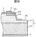
- FIG. 7B is a cross-sectional view taken along the line AA in FIG. 7A.
- FIG. 8A is a plan view showing a Schottky diode according to a third modification of the embodiment of the present invention.
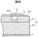
- FIG. 8B is a cross-sectional view taken along the line AA in FIG
- Schottky diode Schottky barrier diode
- FIG. 1 is a diagram schematically showing a cross-sectional configuration of a Schottky diode 1 according to the present embodiment.
- the Schottky diode 1 includes an n-type semiconductor layer 3 made of a Ga 2 O 3 -based compound semiconductor having n-type conductivity, and a Schottky electrode layer in Schottky contact with the first main surface 3 a of the n-type semiconductor layer 3. 2 and an ohmic electrode layer 4 in ohmic contact with the second main surface 3b opposite to the first main surface 3a of the n-type semiconductor layer 3.
- a laminated film including the Schottky electrode layer 2 in the lowermost layer may be provided on the first main surface 3a side of the n-type semiconductor layer 3.
- a laminated film including the ohmic electrode layer 4 in the lowest layer may be provided on the second main surface 3b side of the n-type semiconductor layer 3.
- the n-type semiconductor layer 3 is based on ⁇ -Ga 2 O 3 , but Ga is added with at least one selected from the group consisting of Cu, Ag, Zn, Cd, Al, In, Si, Ge, and Sn. You may comprise with the oxide which made the main component. More specifically, for example, a gallium oxide represented by (Al x In y Ga (1-xy) ) 2 O 3 (where 0 ⁇ x ⁇ 1, 0 ⁇ y ⁇ 1, 0 ⁇ x + y ⁇ 1) is used. Can be used.
- the n-type semiconductor layer 3 includes an n ⁇ semiconductor layer 31 having a low electron carrier concentration as a first semiconductor layer and a high semiconductor layer as a second semiconductor layer having an electron carrier concentration higher than that of the n ⁇ semiconductor layer 31.
- the n ⁇ semiconductor layer 31 having a low electron carrier concentration is formed on the side of the n-type semiconductor layer 3 that is in Schottky contact with the Schottky electrode layer 2.
- the n-type semiconductor layer 3 is formed by supplying Ga vapor and oxygen-based gas into a vacuum chamber by, for example, MBE (Molecular Beam Epitaxy) method, and forming a ⁇ -Ga 2 O 3 single crystal on a ⁇ -Ga 2 O 3 substrate. Can be formed by epitaxial crystal growth. In order to improve controllability of the low electron carrier concentration, the purity of the Ga raw material is preferably 6N or more.
- This ⁇ -Ga 2 O 3 substrate corresponds to the n + semiconductor layer 32, and the epitaxial layer formed thereon corresponds to the n ⁇ semiconductor layer 31.
- the ⁇ -Ga 2 O 3 substrate can be produced by, for example, an EFG (Edge-defined Film-fed Growth) method.
- the electron carrier concentration of the ⁇ -Ga 2 O 3 substrate (the electron carrier concentration of the n + semiconductor layer 32) is determined by the amount of oxygen defects and Si and other dopants that occur during the substrate fabrication.
- the dopant is preferably Si in which the amount of dopant incorporated during crystal growth is stable.
- the controllability of the electron carrier concentration is increased by using Si as a dopant.
- the electron carrier concentration of the n ⁇ semiconductor layer 31 can be adjusted by controlling the supply amount of an IV group dopant such as Si or Sn or oxygen defects during epitaxial crystal growth, for example. Further, when considering substitution with Ga, Sn having a close ionic radius is preferable.
- the electron carrier concentration Nd of the n ⁇ semiconductor layer 31 is, for example, 10 16 cm ⁇ 3 , but this electron carrier concentration Nd is in a range lower than 10 18 cm ⁇ 3. Can be set.
- the electron carrier concentration Nd is preferably set to a value lower than 10 17 cm ⁇ 3 .
- the n ⁇ semiconductor layer 31 may be constituted by an n ⁇ layer having a relatively low electron carrier concentration and an n layer having an electron carrier concentration between the n ⁇ layer and the n + semiconductor layer 32.
- the electron carrier concentration Nd of the n ⁇ semiconductor layer 31 can be set based on the reverse breakdown voltage VRM required for the Schottky diode 1 and the electric field breakdown strength Em of Ga 2 O 3 .
- the electric field breakdown strength Em is a value intrinsic to Ga 2 O 3 , and is smaller than the electric field breakdown strength Em of Ga 2 O 3 compared to the electric field breakdown strength of Si or SiC used as a conventional n-type semiconductor material. It has been confirmed by the present inventors that this is larger.
- the reverse breakdown voltage of a Schottky diode is proportional to the square of the electric field breakdown strength and inversely proportional to the electron carrier concentration. Therefore, if the electric field breakdown strength increases, the reverse breakdown voltage increases even if the electron carrier concentration is the same. Further, if the reverse breakdown voltage is the same, the electron carrier concentration can be increased by increasing the electric field breakdown strength. As the electron carrier concentration increases, the electrical resistance decreases and the forward voltage (VF) decreases.
- FIG. 2A to 2D show the electron carrier concentration and resistance of the n ⁇ semiconductor layer (epitaxial layer) and n + semiconductor layer (substrate) when Si or SiC is used as the semiconductor material and when Ga 2 O 3 is used.
- FIG. 2A is a comparison table showing the relationship between the rate, thickness, and voltage drop when the current density is 200 A / cm 2
- FIG. 2A is a comparison when the reverse breakdown voltage is 100 V using Si and Ga 2 O 3.
- Figure 2C is a case where the reverse breakdown voltage with SiC and Ga 2 O 3 1000V and (1 kV)
- FIG. 2D is a comparison table when SiC and Ga 2 O 3 are used and the reverse breakdown voltage is 10000 V (10 kV).
- the electron carrier concentration and thickness of the n ⁇ semiconductor layer are 2.47 ⁇ 10 15 cm ⁇ 3 and 7.5 ⁇ m for Si, In Ga 2 O 3 according to the present embodiment, it is 8.29 ⁇ 10 17 cm ⁇ 3 and 0.402 ⁇ m.
- the voltage drop in the n ⁇ semiconductor layer is 0.1955 V in the case of Si, and 0.0005 V in the case of Ga 2 O 3 .
- the total voltage drop including the n ⁇ semiconductor layer and the n + semiconductor layer is 0.2226 V in the case of Si and 0.0811 V in the case of Ga 2 O 3 , and the voltage drop is reduced by about 64%. can do.
- the electron carrier concentration and thickness of the n ⁇ semiconductor layer are 2.16 ⁇ 10 16 cm ⁇ 3 and 5.46 ⁇ m in SiC.
- Ga 2 O 3 according to the present embodiment, it is 1.66 ⁇ 10 17 cm ⁇ 3 and 2.0 ⁇ m.
- the voltage drop in the n ⁇ semiconductor layer is 0.0345 V in the case of SiC, and 0.0107 V in the case of Ga 2 O 3 .
- the total voltage drop including the n ⁇ semiconductor layer and the n + semiconductor layer is 0.0546 V in the case of SiC and 0.0376 V in the case of Ga 2 O 3 , and the voltage drop is reduced by about 31%. can do.
- the electron carrier concentration and thickness of the n ⁇ semiconductor layer are 1.30 ⁇ 10 16 cm ⁇ 3 and 9.1 ⁇ m in SiC.
- Ga 2 O 3 according to the present embodiment, it becomes 9.95 ⁇ 10 16 cm ⁇ 3 and 3.3 ⁇ m.
- the voltage drop in the n ⁇ semiconductor layer is 0.0914 V in the case of SiC, and 0.0296 V in the case of Ga 2 O 3 .
- the total voltage drop including the n ⁇ and n + semiconductor layers is 0.1115 V for SiC and 0.0565 V for Ga 2 O 3 , reducing the voltage drop by about 49%. can do.
- the electron carrier concentration and thickness of the n ⁇ semiconductor layer are 1.30 ⁇ 10 15 cm ⁇ 3 and 90.9 ⁇ m in SiC.
- Ga 2 O 3 according to the present embodiment, it becomes 9.95 ⁇ 10 15 cm ⁇ 3 and 33.3 ⁇ m.
- the voltage drop in the n ⁇ semiconductor layer is 8.118 V in the case of SiC, and 2.9449 V in the case of Ga 2 O 3 .
- the total voltage drop including the n ⁇ semiconductor layer and the n + semiconductor layer is 8.1319 V in the case of SiC and 2.9718 V in the case of Ga 2 O 3 , and the voltage drop is reduced by about 63%. can do.
- the Schottky electrode layer 2 shown in FIG. 1 is formed on the first main surface 3a of the n-type semiconductor layer 3 (n ⁇ semiconductor layer 31) by, for example, EB (Electron Beam) vapor deposition, vacuum vapor deposition, or sputtering. Be filmed.
- EB Electro Beam
- a metal capable of making a Schottky contact with Ga 2 O 3 constituting the n ⁇ semiconductor layer 31 is selected.
- Pt is deposited on the n-type semiconductor layer 3 as the Schottky electrode layer 2.
- the relationship between the electron affinity ⁇ of the semiconductor and the work function ⁇ m of the metal serving as the electrode must be ⁇ ⁇ m .
- metals that satisfy this relationship include V, Mo, Ni, Pd, and the like in addition to Pt according to the present embodiment.
- the ohmic electrode layer 4 is formed on the second main surface 3b of the n-type semiconductor layer 3 (n + semiconductor layer 32) by a vacuum evaporation method or a sputtering method.
- Ti is selected as the material of the ohmic electrode layer 4.
- the work function ⁇ m is smaller than the electron affinity ⁇ of Ga 2 O 3 , other elements may be used as the material of the ohmic electrode layer 4.
- FIG. 3 is a schematic diagram showing an energy band of a Schottky contact portion.
- q is a single electron charge
- phi d is the potential barrier (internal potential).
- the thickness t of the n ⁇ semiconductor layer 31 corresponds to the depletion layer width W when the reverse voltage of the reverse breakdown voltage VRM is applied, and is made larger than the depletion layer width W. .
- the depletion layer width W matches the thickness t of the n ⁇ semiconductor layer 31. This is because if the thickness t of the n ⁇ semiconductor layer 31 is larger than the depletion layer width W, the electrical resistance in the n ⁇ semiconductor layer 31 increases accordingly.
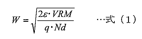
- the depletion layer width W of the Schottky diode 1 depends on the electron carrier concentration Nd of the n ⁇ semiconductor layer 31 as expressed by the following equation (1).
- ⁇ is the dielectric constant of Ga 2 O 3 . That is, if the reverse breakdown voltage VRM and the electron carrier concentration Nd are determined, the depletion layer width W can be obtained.
- the n ⁇ semiconductor layer 31 is formed so that the thickness of epitaxial growth of Ga 2 O 3 having a low electron carrier concentration is equal to or greater than the depletion layer width W (t ⁇ W) with the depletion layer width W as a target.
- the electron carrier concentration of the n + semiconductor layer 32 is set to a necessary concentration (for example, higher than 10 18 cm ⁇ 3 ) according to the electrical resistance (forward ON resistance) or the forward voltage required for the Schottky diode 1. value).
- the electron carrier concentration of the n + semiconductor layer 32 is desirably 10 times or more higher than the electron carrier concentration of the n ⁇ semiconductor layer 31. This is because the electric resistance of the n-type semiconductor layer 3 as a whole becomes smaller as the electron carrier concentration of the n + semiconductor layer 32 is higher.
- a Ga 2 O 3 compound is used as the material for the n-type semiconductor layer 3. Since this Ga 2 O 3 -based compound has a higher electric field breakdown strength than Si and SiC used as a material for conventional Schottky diodes, the reverse breakdown voltage can be increased more than when these conventional materials are used. it can.
- the n-type semiconductor layer 3 is composed of an n ⁇ semiconductor layer 31 having a low electron carrier concentration and an n + semiconductor layer 32 having a high electron carrier concentration.
- the Ga 2 O 3 compound has a high electric field breakdown strength, so that the reverse breakdown voltage can be increased.
- the reverse breakdown voltage is increased. Is inversely proportional to the electron carrier concentration, which limits the effect of increasing the reverse breakdown voltage.
- the n ⁇ semiconductor layer 31 is formed on the Schottky electrode layer 2 side, the reverse breakdown voltage can be further increased.
- the thickness of the n ⁇ semiconductor layer 31 is formed to be thicker than the depletion layer width W when the reverse voltage of the reverse breakdown voltage VRM is applied, the reverse voltage of the reverse breakdown voltage VRM is applied. However, the depletion layer does not reach the n + semiconductor layer 32.
- a reverse breakdown voltage VRM of 1000 V or more can be ensured.
- a reverse breakdown voltage VRM of 10000 V or more can be secured.
- a ⁇ -Ga 2 O 3 substrate having a thickness of 600 ⁇ m manufactured by FZ (Floating Zone) method was used as the n + semiconductor layer 32.
- This ⁇ -Ga 2 O 3 substrate was doped with Si as a dopant, and the electron carrier concentration was 1 ⁇ 10 19 cm ⁇ 3 .
- the plane orientation of the substrate was (010). Although it does not specifically limit about the surface orientation of a board
- the substrate surface orientation may be a surface rotated by an angle of 37.5 ° or less from the (010) plane.
- the interface between the n + semiconductor layer 32 and the n ⁇ semiconductor layer 31 can be made sharp, and the thickness of the n ⁇ semiconductor layer 31 can be controlled with high accuracy.
- the n ⁇ semiconductor layer 31 was formed by epitaxially growing a ⁇ -Ga 2 O 3 single crystal having a thickness of 1.4 ⁇ m on the ⁇ -Ga 2 O 3 substrate (n + semiconductor layer 32) by the MBE method. Sn was used as the dopant, and the electron carrier concentration was 4 ⁇ 10 16 cm ⁇ 3 .
- the Schottky electrode layer 2 has a two-layer structure of 30 nm thick Pt in Schottky contact with the n ⁇ semiconductor layer 31 and 170 nm thick Au formed on the Pt.
- the ohmic electrode layer 4 has a two-layer structure of Ti having a thickness of 100 nm that is in ohmic contact with the n + semiconductor layer 32 and Au having a thickness of 100 nm formed on the Ti.
- FIG. 4 is a diagram schematically showing a cross-sectional configuration of a Schottky diode 10 shown as a comparative example.
- the Schottky diode 10 the ⁇ -Ga 2 O 3 substrate having a thickness of 400 ⁇ m was prepared by the EFG process n - a single layer structure using a semiconductor layer 33, the n - one main surface 33a of the semiconductor layer 33
- the Schottky electrode layer 2 was formed, and the ohmic electrode layer 4 was formed on the other main surface 33b.
- the configurations of the Schottky electrode layer 2 and the ohmic electrode layer 4 are the same as those in the above-described embodiment.
- the n ⁇ semiconductor layer 33 has a thickness of 400 ⁇ m and is not doped and is not subjected to heat treatment in a nitrogen atmosphere, so that the electron carrier concentration is 8 ⁇ 10 16 cm ⁇ 3 .
- FIG. 5 is a graph showing voltage-current density characteristics of the Schottky diode 1 according to the embodiment of the present invention configured as described above and the Schottky diode 10 according to the comparative example. As shown in this figure, in the Schottky diode 1, the current density rises sharply when a positive voltage is applied, whereas in the Schottky diode 10, the current density rises compared to the Schottky diode 1. Has become moderate.
- the semiconductor layer 3 has a multi-layer structure including the n ⁇ semiconductor layer 31 and the n + semiconductor layer 32, and the electrical resistance of the n + semiconductor layer 32 is lowered, so that the forward voltage is reduced. It shows that it was possible.
- the contact resistance between the ohmic electrode 4 and the semiconductor layer 3 is decreased by increasing the electron carrier concentration of the n + semiconductor layer 32 in contact with the ohmic electrode 4, which contributes to reducing the forward voltage. it seems to do.
- Modification 1 6A and 6B show a Schottky diode 1A according to a first modification of the embodiment of the present invention, FIG. 6A is a plan view, and FIG. 6B is a cross-sectional view taken along line AA of FIG. 6A.
- the Schottky diode 1A has a quadrangular shape in a plan view, and the same Schottky electrode layer 2 is formed at the center.
- the Schottky diode 1A includes an n-type semiconductor layer 3.
- the n-type semiconductor layer 3 includes an n ⁇ semiconductor layer 31 having a low electron carrier concentration and a high electron carrier concentration higher than that of the n ⁇ semiconductor layer 31.
- the n ⁇ semiconductor layer 31 having a low electron carrier concentration is formed on the side of the n-type semiconductor layer 3 that is in Schottky contact with the Schottky electrode layer 2.
- An ohmic electrode 4 is formed on the surface of the n + semiconductor layer 32 opposite to the n ⁇ semiconductor layer 31.
- a lower surface 31c parallel to the upper surface 31a is formed outside the side surface 31b so as to surround the side surface 31b.
- the Schottky electrode layer 2 is formed on the upper surface 31a with a predetermined interval between the side surface 31b.
- a PV (passivation) film 6 is formed in a region between the peripheral edge of the Schottky electrode layer 2 and a part on the side surface 31b side of the lower surface 31c.
- the PV film 6 is formed so as to cover a peripheral portion of the Schottky electrode layer 2 and a part of the upper surface 31a, the side surface 31b, and the lower surface 31c on the side surface 31b side of the n + semiconductor layer 32 outside the Schottky electrode layer 2.
- FIG. 7A and 7B show a Schottky diode 1B according to a second modification of the embodiment of the present invention.
- FIG. 7A is a plan view and FIG. 7B is a cross-sectional view taken along line AA of FIG. 7A.
- the Schottky diode 1B is different from the Schottky diode 1A in that the resistance layer 310 is formed in a part of the n ⁇ semiconductor layer 31, and the other configuration is the same as that of the Schottky diode 1A.
- the resistance layer 310 is formed from the portion in contact with the peripheral edge of the Schottky electrode layer 2 on the upper surface 31a side of the n ⁇ semiconductor layer 31 to the side surface 31b.
- the resistance layer 310 can be formed by, for example, annealing in an oxygen atmosphere after forming the n ⁇ semiconductor layer 31 on the n + semiconductor layer 32. Further, this region may be a P-type layer instead of the resistance layer 310.
- the electric field concentration at the end of the Schottky electrode layer 2 is caused by the electric field relaxation effect by the resistance layer 310 or the P-type layer in addition to the electric field relaxation effect by the mesa structure of the n ⁇ semiconductor layer 31. Since it is further relaxed, it is further suppressed that the reverse breakdown voltage decreases due to the electric field concentration at the end of the Schottky electrode layer 2.
- Modification 3 8A and 8B show a Schottky diode 1C according to a third modification of the embodiment of the present invention, FIG. 8A is a plan view, and FIG. 8B is a cross-sectional view taken along line AA of FIG. 8A.
- the Schottky diode 1 ⁇ / b> C has a quadrangular shape in plan view, and includes an n-type semiconductor layer 3 including an n ⁇ semiconductor layer 31 and an n + semiconductor layer 32.
- an n-type semiconductor layer 3 including an n ⁇ semiconductor layer 31 and an n + semiconductor layer 32.
- the PV film 6 is formed on the periphery.
- a Schottky electrode layer 2 is formed at the center of the upper surface 31 a of the n ⁇ semiconductor layer 31.
- the Schottky electrode layer 2 is formed so that a partial region in the peripheral portion covers the PV film 6.
- a resistance layer 310 is formed in a region including the boundary between the Schottky electrode layer 2 and the PV film 6 on the upper surface 31 a side of the n ⁇ semiconductor layer 31. Further, instead of the resistance layer 310, this region may have a guard ring structure made of a P-type layer. Furthermore, the resistance layer 310 and the PV film 6 may have a structure of only the PV film 6 without the resistance layer 310.
- An ohmic electrode 4 is formed on the surface of the n + semiconductor layer 32 opposite to the n ⁇ semiconductor layer 31.
- the electric field concentration at the end of the Schottky electrode layer 2 is alleviated by the field plate effect by the Schottky electrode layer 2 formed on the PV film 6, so that the Schottky electrode
- the reverse breakdown voltage is suppressed from decreasing due to the electric field concentration at the end of the layer 2.
- the resistance layer 310 or the P-type layer is formed, the electric field concentration effect is further relaxed by the electric field relaxation effect, so that the resistance layer 310 or the P-type layer is moved to the end of the Schottky electrode layer 2. It is further suppressed that the reverse breakdown voltage decreases due to the electric field concentration.
- the Schottky diode 1 may be a horizontal type in which the Schottky electrode layer 2 and the ohmic electrode layer 4 are vapor-deposited on the same surface side of the n-type semiconductor layer 3 in addition to the configuration of the above embodiment (vertical type). Good.
- a Schottky barrier diode capable of suppressing an increase in forward voltage and an increase in contact resistance with an ohmic electrode layer even when the reverse breakdown voltage is increased.
Landscapes
- Electrodes Of Semiconductors (AREA)
- Chemical & Material Sciences (AREA)
- Crystallography & Structural Chemistry (AREA)
Abstract
Description
ショットキーダイオード1に対して順方向(ショットキー電極層2側が正電位)に電圧Vを加えると、図3に示すφdが(φd-V)となり、n型半導体層3からショットキー電極層2へ移動する電子による電流が増大する。これにより、順方向電流がショットキー電極層2からオーミック電極層4へ流れる。
本実施の形態によれば、下記の作用効果がある。
図4は、比較例として示すショットキーダイオード10の断面構成を模式的に示す図である。このショットキーダイオード10は、EFG法により作製した厚さ400μmのβ-Ga2O3基板をn-半導体層33として用いた単層構造であり、このn-半導体層33の一方の主面33aにショットキー電極層2を形成し、他方の主面33bにオーミック電極層4を形成した。ショットキー電極層2及びオーミック電極層4の構成は、上記の実施例と共通の構成とした。また、n-半導体層33は、厚さを400μmとし、ノンドープかつ窒素雰囲気熱処理を行わないことで、電子キャリア濃度を8×1016cm-3とした。
次に、本発明の実施の形態に係るショットキーダイオードの構造の3つの変形例を図6A~図8Bを参照して説明する。これらの変形例において、n-半導体層31及びn+半導体層32のキャリア濃度及び厚み等の諸元は、上記説明したものと同様に設定することができる。
図6Aおよび図6Bは、本発明の実施の形態の第1の変形例に係るショットキーダイオード1Aを示し、図6Aは平面図、図6Bは図6AのA-A断面図である。
図7Aおよび図7Bは、本発明の実施の形態の第2の変形例に係るショットキーダイオード1Bを示し、図7Aは平面図、図7Bは図7AのA-A断面図である。
図8Aおよび図8Bは、本発明の実施の形態の第3の変形例に係るショットキーダイオード1Cを示し、図8Aは平面図、図8Bは図8AのA-A断面図である。
Claims (5)
- n型の導電性を有するGa2O3系化合物半導体からなるn型半導体層と、前記n型半導体層に対してショットキー接触する電極層とを備え、
前記n型半導体層には、前記電極層にショットキー接触する第1の半導体層と、前記第1の半導体層よりも高い電子キャリア濃度を有する第2の半導体層とが形成されているショットキーバリアダイオード。 - 前記第1の半導体層の厚みは、逆方向耐圧に対応する空乏層の厚みよりも大きい請求項1に記載のショットキーバリアダイオード。
- 前記第1の半導体層における電子キャリア濃度が1×1017cm-3よりも低い請求項1又は2に記載のショットキーバリアダイオード。
- 前記第2の半導体層における電子キャリア濃度が1×1018cm-3よりも高い請求項1又は2に記載のショットキーバリアダイオード。
- 前記第2の半導体層における電子キャリア濃度が1×1018cm-3よりも高い請求項3に記載のショットキーバリアダイオード。
Priority Applications (11)
| Application Number | Priority Date | Filing Date | Title |
|---|---|---|---|
| EP12848460.7A EP2779242A4 (en) | 2011-11-09 | 2012-11-08 | SCHOTTKY BARRIER DIODE |
| KR1020207002030A KR102191283B1 (ko) | 2011-11-09 | 2012-11-08 | 쇼트키 배리어 다이오드 |
| KR1020197022358A KR102070847B1 (ko) | 2011-11-09 | 2012-11-08 | 쇼트키 배리어 다이오드 |
| US14/357,176 US9171967B2 (en) | 2011-11-09 | 2012-11-08 | Schottky barrier diode |
| KR1020147014887A KR102025449B1 (ko) | 2011-11-09 | 2012-11-08 | 쇼트키 배리어 다이오드 |
| CN201280054764.8A CN103918082B (zh) | 2011-11-09 | 2012-11-08 | 肖特基势垒二极管 |
| US14/918,129 US9412882B2 (en) | 2011-11-09 | 2015-10-20 | Schottky barrier diode |
| US15/208,469 US9595586B2 (en) | 2011-11-09 | 2016-07-12 | Schottky barrier diode |
| US15/436,508 US10600874B2 (en) | 2011-11-09 | 2017-02-17 | Schottky barrier diode |
| US16/801,993 US11264466B2 (en) | 2011-11-09 | 2020-02-26 | Schottky barrier diode |
| US17/582,924 US12557361B2 (en) | 2011-11-09 | 2022-01-24 | Schottky barrier diode with high withstand voltage |
Applications Claiming Priority (2)
| Application Number | Priority Date | Filing Date | Title |
|---|---|---|---|
| JP2011245519A JP2013102081A (ja) | 2011-11-09 | 2011-11-09 | ショットキーバリアダイオード |
| JP2011-245519 | 2011-11-09 |
Related Child Applications (2)
| Application Number | Title | Priority Date | Filing Date |
|---|---|---|---|
| US14/357,176 A-371-Of-International US9171967B2 (en) | 2011-11-09 | 2012-11-08 | Schottky barrier diode |
| US14/918,129 Continuation US9412882B2 (en) | 2011-11-09 | 2015-10-20 | Schottky barrier diode |
Publications (1)
| Publication Number | Publication Date |
|---|---|
| WO2013069728A1 true WO2013069728A1 (ja) | 2013-05-16 |
Family
ID=48290098
Family Applications (1)
| Application Number | Title | Priority Date | Filing Date |
|---|---|---|---|
| PCT/JP2012/078983 Ceased WO2013069728A1 (ja) | 2011-11-09 | 2012-11-08 | ショットキーバリアダイオード |
Country Status (7)
| Country | Link |
|---|---|
| US (6) | US9171967B2 (ja) |
| EP (1) | EP2779242A4 (ja) |
| JP (1) | JP2013102081A (ja) |
| KR (3) | KR102191283B1 (ja) |
| CN (2) | CN110233178A (ja) |
| TW (2) | TWI627748B (ja) |
| WO (1) | WO2013069728A1 (ja) |
Cited By (2)
| Publication number | Priority date | Publication date | Assignee | Title |
|---|---|---|---|---|
| CN110085681A (zh) * | 2019-05-20 | 2019-08-02 | 中山大学 | 一种氧化镓基异质pn结二极管及其制备方法 |
| JP2020502801A (ja) * | 2016-12-15 | 2020-01-23 | グリフィス・ユニバーシティGriffith University | 炭化シリコンショットキーダイオード |
Families Citing this family (50)
| Publication number | Priority date | Publication date | Assignee | Title |
|---|---|---|---|---|
| KR102267094B1 (ko) * | 2013-08-19 | 2021-06-18 | 이데미쓰 고산 가부시키가이샤 | 산화물 반도체 기판 및 쇼트키 배리어 다이오드 |
| JPWO2015025499A1 (ja) * | 2013-08-19 | 2017-03-02 | 出光興産株式会社 | 酸化物半導体基板及びショットキーバリアダイオード |
| CN106415845B (zh) * | 2014-07-22 | 2019-12-10 | 株式会社Flosfia | 结晶性半导体膜和板状体以及半导体装置 |
| JP2016031953A (ja) | 2014-07-25 | 2016-03-07 | 株式会社タムラ製作所 | 半導体素子及びその製造方法、半導体基板、並びに結晶積層構造体 |
| JP6260553B2 (ja) * | 2015-02-27 | 2018-01-17 | 豊田合成株式会社 | 半導体装置およびその製造方法 |
| JP6758569B2 (ja) * | 2015-03-20 | 2020-09-23 | 株式会社タムラ製作所 | 高耐圧ショットキーバリアダイオード |
| JP2017045969A (ja) * | 2015-08-28 | 2017-03-02 | 株式会社タムラ製作所 | ショットキーバリアダイオード |
| JP6744523B2 (ja) * | 2015-12-16 | 2020-08-19 | 株式会社タムラ製作所 | 半導体基板、並びにエピタキシャルウエハ及びその製造方法 |
| CN107068773B (zh) | 2015-12-18 | 2021-06-01 | 株式会社Flosfia | 半导体装置 |
| TWI726964B (zh) | 2015-12-25 | 2021-05-11 | 日商出光興產股份有限公司 | 積層體 |
| KR102382656B1 (ko) | 2015-12-25 | 2022-04-04 | 이데미쓰 고산 가부시키가이샤 | 적층체 |
| JP6975530B2 (ja) * | 2015-12-25 | 2021-12-01 | 出光興産株式会社 | 半導体素子及びそれを用いた電気機器 |
| JP2017139289A (ja) | 2016-02-02 | 2017-08-10 | トヨタ自動車株式会社 | ダイオード |
| JP2017139293A (ja) * | 2016-02-02 | 2017-08-10 | トヨタ自動車株式会社 | ダイオード |
| JP6845397B2 (ja) | 2016-04-28 | 2021-03-17 | 株式会社タムラ製作所 | トレンチmos型ショットキーダイオード |
| JP7433611B2 (ja) * | 2016-04-28 | 2024-02-20 | 株式会社タムラ製作所 | トレンチmos型ショットキーダイオード |
| WO2018020849A1 (ja) * | 2016-07-26 | 2018-02-01 | 三菱電機株式会社 | 半導体装置および半導体装置の製造方法 |
| CN109643660B (zh) * | 2016-08-31 | 2024-03-05 | 株式会社Flosfia | p-型氧化物半导体及其制造方法 |
| US20180097073A1 (en) * | 2016-10-03 | 2018-04-05 | Flosfia Inc. | Semiconductor device and semiconductor system including semiconductor device |
| JP6812758B2 (ja) * | 2016-11-09 | 2021-01-13 | Tdk株式会社 | ショットキーバリアダイオード及びこれを備える電子回路 |
| CN106935661B (zh) * | 2017-01-23 | 2019-07-16 | 西安电子科技大学 | 垂直型肖特基二极管及其制作方法 |
| CN106876484B (zh) * | 2017-01-23 | 2019-10-11 | 西安电子科技大学 | 高击穿电压氧化镓肖特基二极管及其制作方法 |
| JP6558385B2 (ja) * | 2017-02-23 | 2019-08-14 | トヨタ自動車株式会社 | 半導体装置の製造方法 |
| JP7116409B2 (ja) | 2017-02-27 | 2022-08-10 | 株式会社タムラ製作所 | トレンチmos型ショットキーダイオード |
| TWI641152B (zh) * | 2017-03-24 | 2018-11-11 | 王中林 | 電壓增加而電阻值增加的電阻元件 |
| JP6809334B2 (ja) * | 2017-03-29 | 2021-01-06 | Tdk株式会社 | 半導体装置及びその製造方法 |
| JP7008293B2 (ja) * | 2017-04-27 | 2022-01-25 | 国立研究開発法人情報通信研究機構 | Ga2O3系半導体素子 |
| CN110809826B (zh) * | 2017-06-29 | 2022-10-28 | 三菱电机株式会社 | 氧化物半导体装置以及氧化物半导体装置的制造方法 |
| JP7037142B2 (ja) * | 2017-08-10 | 2022-03-16 | 株式会社タムラ製作所 | ダイオード |
| JP7147141B2 (ja) * | 2017-09-11 | 2022-10-05 | Tdk株式会社 | ショットキーバリアダイオード |
| CN108597985B (zh) * | 2018-04-17 | 2020-12-22 | 中山大学 | 一种叠层结构 |
| JPWO2020013244A1 (ja) * | 2018-07-12 | 2021-07-15 | 株式会社Flosfia | 半導体装置 |
| KR102371319B1 (ko) | 2019-04-16 | 2022-03-07 | 한국전자통신연구원 | 쇼트키 장벽 다이오드 및 그의 제조 방법 |
| KR102275146B1 (ko) * | 2019-05-20 | 2021-07-08 | 파워큐브세미 (주) | 쇼트키 다이오드 및 그의 제조방법 |
| CN110265486B (zh) | 2019-06-20 | 2023-03-24 | 中国电子科技集团公司第十三研究所 | 氧化镓sbd终端结构及制备方法 |
| JP7612136B2 (ja) * | 2019-10-03 | 2025-01-14 | 株式会社Flosfia | 半導体素子および半導体装置 |
| JP7391326B2 (ja) * | 2019-12-26 | 2023-12-05 | 株式会社ノベルクリスタルテクノロジー | 半導体装置 |
| KR102335550B1 (ko) | 2020-05-06 | 2021-12-08 | 파워큐브세미 (주) | 멀티에피를 활용하여 러기드니스가 강화된 실리콘카바이드 정션 배리어 쇼트키 다이오드 |
| US11342484B2 (en) | 2020-05-11 | 2022-05-24 | Silanna UV Technologies Pte Ltd | Metal oxide semiconductor-based light emitting device |
| JP7469201B2 (ja) | 2020-09-18 | 2024-04-16 | 株式会社デンソー | 半導体装置とその製造方法 |
| JP7442428B2 (ja) * | 2020-12-11 | 2024-03-04 | 株式会社デンソー | 半導体装置の製造方法 |
| JP2022187481A (ja) * | 2021-06-07 | 2022-12-19 | 株式会社Flosfia | 半導体装置 |
| EP4423325A4 (en) | 2021-10-27 | 2025-08-27 | Silanna UV Technologies Pte Ltd | METHODS AND SYSTEMS FOR HEATING A WIDE BANDGAP SUBSTRATE |
| EP4430674A4 (en) | 2021-11-10 | 2025-10-01 | Silanna UV Technologies Pte Ltd | EPITAXIAL OXIDE MATERIALS, STRUCTURES AND DEVICES |
| JP7829033B2 (ja) | 2021-11-10 | 2026-03-12 | シランナ・ユー・ブイ・テクノロジーズ・プライベート・リミテッド | 酸化マグネシウムゲルマニウムを含む超ワイドバンドギャップ半導体デバイス |
| JP7814510B2 (ja) | 2021-11-10 | 2026-02-16 | シランナ・ユー・ブイ・テクノロジーズ・プライベート・リミテッド | エピタキシャル酸化物材料、構造、及びデバイス |
| JPWO2024005152A1 (ja) * | 2022-06-29 | 2024-01-04 | ||
| CN117954504A (zh) * | 2022-10-19 | 2024-04-30 | 广州华瑞升阳投资有限公司 | 一种肖特基势垒二极管 |
| EP4404277A4 (en) * | 2022-12-06 | 2024-10-23 | Shindengen Electric Manufacturing Co., Ltd. | SCHOTTKY BARRIER DIODE |
| CN116344626B (zh) * | 2023-05-16 | 2024-06-18 | 重庆邮电大学 | 具有斜面终端的沟槽氧化镓异质结二极管 |
Citations (3)
| Publication number | Priority date | Publication date | Assignee | Title |
|---|---|---|---|---|
| JP2006253521A (ja) | 2005-03-14 | 2006-09-21 | Kansai Tlo Kk | 半導体ダイオード装置及びその製造方法 |
| JP2009200222A (ja) * | 2008-02-21 | 2009-09-03 | Nippon Light Metal Co Ltd | 紫外線センサ及びその製造方法 |
| JP2010233406A (ja) * | 2009-03-27 | 2010-10-14 | Koha Co Ltd | スイッチング制御装置及びショットキーダイオード |
Family Cites Families (20)
| Publication number | Priority date | Publication date | Assignee | Title |
|---|---|---|---|---|
| US5686753A (en) * | 1994-11-11 | 1997-11-11 | Murata Manufacturing Co., Ltd. | Schottky barrier diode having a mesa structure |
| JP3123452B2 (ja) | 1996-12-10 | 2001-01-09 | 富士電機株式会社 | ショットキーバリアダイオード |
| US6184563B1 (en) * | 1998-07-27 | 2001-02-06 | Ho-Yuan Yu | Device structure for providing improved Schottky barrier rectifier |
| JP4100652B2 (ja) | 1999-08-10 | 2008-06-11 | 富士電機デバイステクノロジー株式会社 | SiCショットキーダイオード |
| KR100348269B1 (ko) * | 2000-03-22 | 2002-08-09 | 엘지전자 주식회사 | 루데니움 산화물을 이용한 쇼트키 콘택 방법 |
| US20030015708A1 (en) | 2001-07-23 | 2003-01-23 | Primit Parikh | Gallium nitride based diodes with low forward voltage and low reverse current operation |
| KR100787272B1 (ko) | 2003-02-24 | 2007-12-20 | 각코호진 와세다다이가쿠 | Ga2O3계 발광 소자 및 그 제조 방법 |
| JP4630986B2 (ja) * | 2003-02-24 | 2011-02-09 | 学校法人早稲田大学 | β−Ga2O3系単結晶成長方法 |
| JP4670034B2 (ja) * | 2004-03-12 | 2011-04-13 | 学校法人早稲田大学 | 電極を備えたGa2O3系半導体層 |
| TWI375994B (en) * | 2004-09-01 | 2012-11-01 | Sumitomo Electric Industries | Epitaxial substrate and semiconductor element |
| JP2006100801A (ja) | 2004-09-01 | 2006-04-13 | Sumitomo Electric Ind Ltd | エピタキシャル基板および半導体素子 |
| JP5303819B2 (ja) * | 2005-08-05 | 2013-10-02 | 住友電気工業株式会社 | 半導体装置およびその製造方法 |
| JP5052807B2 (ja) | 2006-03-29 | 2012-10-17 | 古河電気工業株式会社 | 半導体装置及び電力変換装置 |
| JP2008034572A (ja) | 2006-07-28 | 2008-02-14 | Matsushita Electric Ind Co Ltd | 半導体装置とその製造方法 |
| JP4730422B2 (ja) | 2008-10-24 | 2011-07-20 | 住友電気工業株式会社 | Iii族窒化物半導体電子デバイス、iii族窒化物半導体電子デバイスを作製する方法、及びiii族窒化物半導体エピタキシャルウエハ |
| JP2011176090A (ja) * | 2010-02-24 | 2011-09-08 | Nippon Light Metal Co Ltd | 紫外線センサ、およびその製造方法 |
| JP5543672B2 (ja) * | 2011-09-08 | 2014-07-09 | 株式会社タムラ製作所 | 結晶積層構造体 |
| WO2013035464A1 (ja) | 2011-09-08 | 2013-03-14 | 株式会社タムラ製作所 | 結晶積層構造体及びその製造方法 |
| JP5857337B2 (ja) * | 2011-09-21 | 2016-02-10 | 並木精密宝石株式会社 | 酸化ガリウム基板とその製造方法 |
| US9304396B2 (en) | 2013-02-25 | 2016-04-05 | Lam Research Corporation | PECVD films for EUV lithography |
-
2011
- 2011-11-09 JP JP2011245519A patent/JP2013102081A/ja active Pending
-
2012
- 2012-11-08 KR KR1020207002030A patent/KR102191283B1/ko active Active
- 2012-11-08 KR KR1020147014887A patent/KR102025449B1/ko active Active
- 2012-11-08 US US14/357,176 patent/US9171967B2/en active Active
- 2012-11-08 KR KR1020197022358A patent/KR102070847B1/ko active Active
- 2012-11-08 CN CN201910677483.1A patent/CN110233178A/zh active Pending
- 2012-11-08 WO PCT/JP2012/078983 patent/WO2013069728A1/ja not_active Ceased
- 2012-11-08 EP EP12848460.7A patent/EP2779242A4/en not_active Withdrawn
- 2012-11-08 CN CN201280054764.8A patent/CN103918082B/zh active Active
- 2012-11-09 TW TW105119585A patent/TWI627748B/zh active
- 2012-11-09 TW TW101141829A patent/TWI585973B/zh active
-
2015
- 2015-10-20 US US14/918,129 patent/US9412882B2/en active Active
-
2016
- 2016-07-12 US US15/208,469 patent/US9595586B2/en active Active
-
2017
- 2017-02-17 US US15/436,508 patent/US10600874B2/en active Active
-
2020
- 2020-02-26 US US16/801,993 patent/US11264466B2/en active Active
-
2022
- 2022-01-24 US US17/582,924 patent/US12557361B2/en active Active
Patent Citations (3)
| Publication number | Priority date | Publication date | Assignee | Title |
|---|---|---|---|---|
| JP2006253521A (ja) | 2005-03-14 | 2006-09-21 | Kansai Tlo Kk | 半導体ダイオード装置及びその製造方法 |
| JP2009200222A (ja) * | 2008-02-21 | 2009-09-03 | Nippon Light Metal Co Ltd | 紫外線センサ及びその製造方法 |
| JP2010233406A (ja) * | 2009-03-27 | 2010-10-14 | Koha Co Ltd | スイッチング制御装置及びショットキーダイオード |
Non-Patent Citations (1)
| Title |
|---|
| See also references of EP2779242A4 |
Cited By (3)
| Publication number | Priority date | Publication date | Assignee | Title |
|---|---|---|---|---|
| JP2020502801A (ja) * | 2016-12-15 | 2020-01-23 | グリフィス・ユニバーシティGriffith University | 炭化シリコンショットキーダイオード |
| JP7112099B2 (ja) | 2016-12-15 | 2022-08-03 | グリフィス・ユニバーシティ | 炭化シリコンショットキーダイオード |
| CN110085681A (zh) * | 2019-05-20 | 2019-08-02 | 中山大学 | 一种氧化镓基异质pn结二极管及其制备方法 |
Also Published As
| Publication number | Publication date |
|---|---|
| US12557361B2 (en) | 2026-02-17 |
| US20160322467A1 (en) | 2016-11-03 |
| EP2779242A1 (en) | 2014-09-17 |
| TW201338155A (zh) | 2013-09-16 |
| TWI585973B (zh) | 2017-06-01 |
| KR20190094249A (ko) | 2019-08-12 |
| US20160043238A1 (en) | 2016-02-11 |
| US10600874B2 (en) | 2020-03-24 |
| US20140332823A1 (en) | 2014-11-13 |
| US9171967B2 (en) | 2015-10-27 |
| US20220149158A1 (en) | 2022-05-12 |
| TW201703255A (zh) | 2017-01-16 |
| KR102070847B1 (ko) | 2020-01-30 |
| CN103918082B (zh) | 2019-08-20 |
| US20200194560A1 (en) | 2020-06-18 |
| EP2779242A4 (en) | 2015-03-25 |
| TWI627748B (zh) | 2018-06-21 |
| CN103918082A (zh) | 2014-07-09 |
| KR20200011561A (ko) | 2020-02-03 |
| US20170162655A1 (en) | 2017-06-08 |
| US11264466B2 (en) | 2022-03-01 |
| KR20140095080A (ko) | 2014-07-31 |
| KR102191283B1 (ko) | 2020-12-15 |
| JP2013102081A (ja) | 2013-05-23 |
| CN110233178A (zh) | 2019-09-13 |
| US9412882B2 (en) | 2016-08-09 |
| US9595586B2 (en) | 2017-03-14 |
| KR102025449B1 (ko) | 2019-09-25 |
Similar Documents
| Publication | Publication Date | Title |
|---|---|---|
| US12557361B2 (en) | Schottky barrier diode with high withstand voltage | |
| JP7349672B2 (ja) | ショットキーバリアダイオード及びpn接合部 | |
| JP4872158B2 (ja) | ショットキーダイオード、pn接合ダイオード、pin接合ダイオード、および製造方法 | |
| US9171914B2 (en) | Semiconductor device | |
| US11728393B2 (en) | Semiconductor device | |
| WO2018010545A1 (zh) | 一种异质结终端的碳化硅功率器件及其制备方法 | |
| KR102745528B1 (ko) | 산화니켈-산화갈륨 이종접합 다이오드 제조 방법 | |
| JP7142047B2 (ja) | ショットキーバリアダイオード | |
| JP6204436B2 (ja) | ショットキーバリアダイオード | |
| JP6673984B2 (ja) | ショットキーバリアダイオード | |
| JP6367436B2 (ja) | ショットキーバリアダイオード |
Legal Events
| Date | Code | Title | Description |
|---|---|---|---|
| 121 | Ep: the epo has been informed by wipo that ep was designated in this application |
Ref document number: 12848460 Country of ref document: EP Kind code of ref document: A1 |
|
| WWE | Wipo information: entry into national phase |
Ref document number: 14357176 Country of ref document: US |
|
| NENP | Non-entry into the national phase |
Ref country code: DE |
|
| WWE | Wipo information: entry into national phase |
Ref document number: 2012848460 Country of ref document: EP |
|
| ENP | Entry into the national phase |
Ref document number: 20147014887 Country of ref document: KR Kind code of ref document: A |