WO2013077237A1 - Module de source de lumière, dispositif électronique le comportant et dispositif d'affichage à cristaux liquides - Google Patents
Module de source de lumière, dispositif électronique le comportant et dispositif d'affichage à cristaux liquides Download PDFInfo
- Publication number
- WO2013077237A1 WO2013077237A1 PCT/JP2012/079593 JP2012079593W WO2013077237A1 WO 2013077237 A1 WO2013077237 A1 WO 2013077237A1 JP 2012079593 W JP2012079593 W JP 2012079593W WO 2013077237 A1 WO2013077237 A1 WO 2013077237A1
- Authority
- WO
- WIPO (PCT)
- Prior art keywords
- light
- guide member
- light guide
- light source
- source module
- Prior art date
- Legal status (The legal status is an assumption and is not a legal conclusion. Google has not performed a legal analysis and makes no representation as to the accuracy of the status listed.)
- Ceased
Links
Images






Classifications
-
- G—PHYSICS
- G02—OPTICS
- G02B—OPTICAL ELEMENTS, SYSTEMS OR APPARATUS
- G02B6/00—Light guides; Structural details of arrangements comprising light guides and other optical elements, e.g. couplings
- G02B6/0001—Light guides; Structural details of arrangements comprising light guides and other optical elements, e.g. couplings specially adapted for lighting devices or systems
- G02B6/0011—Light guides; Structural details of arrangements comprising light guides and other optical elements, e.g. couplings specially adapted for lighting devices or systems the light guides being planar or of plate-like form
- G02B6/0033—Means for improving the coupling-out of light from the light guide
- G02B6/0035—Means for improving the coupling-out of light from the light guide provided on the surface of the light guide or in the bulk of it
- G02B6/004—Scattering dots or dot-like elements, e.g. microbeads, scattering particles, nanoparticles
- G02B6/0043—Scattering dots or dot-like elements, e.g. microbeads, scattering particles, nanoparticles provided on the surface of the light guide
-
- G—PHYSICS
- G02—OPTICS
- G02B—OPTICAL ELEMENTS, SYSTEMS OR APPARATUS
- G02B6/00—Light guides; Structural details of arrangements comprising light guides and other optical elements, e.g. couplings
- G02B6/0001—Light guides; Structural details of arrangements comprising light guides and other optical elements, e.g. couplings specially adapted for lighting devices or systems
- G02B6/0011—Light guides; Structural details of arrangements comprising light guides and other optical elements, e.g. couplings specially adapted for lighting devices or systems the light guides being planar or of plate-like form
- G02B6/0033—Means for improving the coupling-out of light from the light guide
- G02B6/0058—Means for improving the coupling-out of light from the light guide varying in density, size, shape or depth along the light guide
-
- G—PHYSICS
- G02—OPTICS
- G02B—OPTICAL ELEMENTS, SYSTEMS OR APPARATUS
- G02B6/00—Light guides; Structural details of arrangements comprising light guides and other optical elements, e.g. couplings
- G02B6/0001—Light guides; Structural details of arrangements comprising light guides and other optical elements, e.g. couplings specially adapted for lighting devices or systems
- G02B6/0011—Light guides; Structural details of arrangements comprising light guides and other optical elements, e.g. couplings specially adapted for lighting devices or systems the light guides being planar or of plate-like form
- G02B6/0033—Means for improving the coupling-out of light from the light guide
- G02B6/0058—Means for improving the coupling-out of light from the light guide varying in density, size, shape or depth along the light guide
- G02B6/0061—Means for improving the coupling-out of light from the light guide varying in density, size, shape or depth along the light guide to provide homogeneous light output intensity
Definitions
- the present invention relates to a light source module, and an electronic apparatus and a liquid crystal display device including the light source module.
- Liquid crystal display devices such as liquid crystal televisions are used in various fields because they are suitable for thinning and weight reduction.
- the liquid crystal display device includes a light source module called a backlight that irradiates a liquid crystal panel from the back side.
- a backlight that emits light from a light source in a planar shape by a light guide member has been attracting attention because it is more suitable for thinning than other types.
- the light source of the backlight for example, an LED (Light Emitting Diode) is used.
- Examples of the backlight using the light guide member include those described in Patent Document 1.
- FIG. 10 is a cross-sectional view showing the configuration of the light source module 200 described in Patent Document 1.
- a light source 202 for coupling light to the light guide member 201 is disposed on the end surface 201 ⁇ / b> A of the light guide member 201.
- a light diffusion structure 204 having a plurality of light diffusion portions 204A for diffusing the combined light is provided on at least one of the back surface 201C and the light emission surface 201D of the light guide member 201.
- the light emitted from the light source 202 is coupled into the light guide member 201 and propagates while repeating total reflection inside. At this time, when the total reflection condition is broken by the light diffusion structure 204 formed on the light guide member 201, the light is emitted from the light guide member 201.
- the density of the light diffusion structure 204 which is the ratio of the dimension in the light guide direction of the light diffusion portion 204A per unit dimension in the light guide direction, is defined as the coupling end surface 201A. It is disclosed that the position of the light guide member 201 is increased to a position at least one-half of the dimension of the light guide member 201 from the position to the surface 201B facing the coupling end surface. At the same time, the light diffusing structure 204 is constant or reduced in a region exceeding one-half or more of the dimension of the light guide member 201 from the position of the coupling end surface 201A to the surface 201B facing the coupling end surface. Is disclosed.
- the interval between the reflective portions formed on the light guide plate changes in the direction from the upper side to the lower side of the light guide plate and in the direction from the left and right sides to the center side. ing.
- the backlight device disclosed in Patent Document 3 includes a plurality of LEDs and a diffusion plate that receives light emitted from the plurality of LEDs and imparts a diffusing action to the incident light.
- the plurality of LEDs are arranged with a non-uniform arrangement density on a predetermined surface.
- Patent Document 4 discloses a linear light source device composed of a plurality of LED chips.
- Patent Document 5 discloses a technique related to a plurality of LEDs arranged in a line on the side surface of a light guide plate. According to the technique of Patent Document 5, a plurality of LEDs are ranked based on luminance, an LED having a luminance rank of “high” is arranged in the center, and a luminance rank of “low” is arranged on the end side. LEDs are arranged.
- Patent No. 4565030 (issued on October 20, 2010) JP 2010-282911 A (released on December 16, 2010) JP 2010-049994 A (published March 4, 2010) JP 2010-015709 A (released January 21, 2010) JP 2006-267780 A (published October 5, 2006)
- the density of the light diffusion structure 204 is constant in the direction perpendicular to the light guide direction.
- the luminance distribution in the direction perpendicular to the light guide direction varies in luminance within the light source, and the light incident from the light source It is affected by the spread within the light guide member.
- light scattered by the light diffusing structure and satisfying the total reflection condition is guided and spreads in the light guide member, so that it is also affected by the spread of the light. Therefore, in the light source module of Patent Document 1, when the density of the light diffusion structure 204 is constant in the direction perpendicular to the light guide direction, there remains a problem that the screen quality is deteriorated. This problem will be described in more detail.
- the luminance distribution of the backlight increases the luminance at the center of the screen and decreases the luminance at the periphery to a bow to achieve both low power consumption and improved screen quality.
- Brightness distribution The reason why the peripheral portion is lowered like a bow is to improve the screen quality by smoothly reducing the luminance distribution so that it is not visually recognized as luminance unevenness. Therefore, when the luminance distribution of the backlight is not smooth, it is visually recognized as luminance unevenness, and the screen quality is deteriorated.
- FIG. 9A to 9C show the results of analyzing the luminance distribution of the backlight using the light guide member 201 in which the density of the light diffusion structure 204 shown in FIG. 10 is constant in the direction perpendicular to the light guide direction. Show.
- the luminance distribution is not smooth, and the luminance is in some places.
- the distribution is wavy.
- Such a luminance distribution is visually recognized as luminance unevenness, and the screen quality is deteriorated.
- the present invention has been made in view of the above problems, and its purpose is to realize a luminance distribution in which the luminance is high in the central portion and perpendicular to the light guiding direction and decreases in a bow-like manner from the central portion toward the peripheral portion. It is possible to provide a light source module that can be used and has excellent screen quality, and an electronic device and a liquid crystal display device including the light source module.
- the inventors of the present application have found that the luminance distribution can be realized if the density distribution of the light diffusion structure has at least three extreme values in the direction perpendicular to the light guide direction, and the present invention has been achieved.
- the light source module of the present invention includes a light source, a first end surface on which light from the light source is incident, a second end surface opposite to the first end surface, A light guide member that is located between the first and second end faces and has an emission surface that emits light from the first end face; and light that is guided from the first end face into the light guide member.
- a light diffusing structure that includes a plurality of light diffusing portions to be diffused and formed on at least one of the light exit surface and the back surface on the opposite side, and viewed from the light exit surface side and second from the first end surface
- the density distribution of the light diffusion structure has at least an extreme value in the second direction. It is characterized by having three.
- the “extreme value” here is a value when the gradient of the tangent is 0 when the density distribution of the light diffusion structure is approximated as a function of a curve, and includes “maximum value” and “minimum value”. .
- the “density distribution of the light diffusing structure” includes “the dot diameter distribution of the light diffusing portion” and “the distribution of the distance between the centers of the adjacent light diffusing portions”.
- the direction which goes to a 2nd end surface from a 1st end surface is made into the 1st direction, and the direction perpendicular
- the density distribution of the light diffusing structure has at least three extreme values in the second direction, the luminance is high in the central part in the direction perpendicular to the light guiding direction, and the density increases from the central part to the peripheral part. Accordingly, it is possible to provide a light source module that realizes a luminance distribution that decreases like a bow and has excellent screen quality.
- the density distribution in the second direction of the light diffusing structure has a maximum value at the center of the light guide member in the second direction, and on both sides of the second direction across the maximum value. It is preferable to have a local minimum.
- the density distribution in the second direction of the light diffusing structure has a minimum value in the vicinity of both ends of the light guide member in the second direction, and corresponds to the minimum value.
- the density increases from the position in the second direction toward the end in the second direction.
- the minimum value of the density distribution in the second direction of the light diffusion structure is H
- the minimum value of the density distribution in the second direction of the light diffusion structure is It is preferable that the light guide member exists in a region from both ends in the second direction to H / 3.
- the density distribution in the second direction of the light diffusion structure has a minimum value, and the density change rate before and after the minimum value changes in the first direction, It is preferable that a maximum value exists between the central portion of the light guide member in the first direction and the second end surface.
- the density change rate before and behind the said minimum value is changing in the said 1st direction,
- the density distribution of the light diffusion structure is a distribution that takes into account the spread of light in the first direction in addition to the second direction. Therefore, according to the above configuration, it is possible to achieve a smooth distribution such as a Gaussian distribution or a quadratic function for the luminance distribution in the second direction at each location in the first direction of the light guide member. it can.
- the p is the following formula (1), p ⁇ 2.5t / 3 Formula (1) It is preferable to satisfy.
- the maximum value p max of the center-to-center distance between the adjacent light diffusion parts may be applied to the above equation (1). That is, when the thickness of the light guide member is t, p max is expressed by the following formula (1 ′), p max ⁇ 2.5t / 3 Formula (1 ′) Should be satisfied.
- the density of the light diffusion structure occupying a unit area of the emission surface is 0.4% / unit or more and 67% / unit or less.
- the distance between the light diffusion portions can be set to a certain value or more while suppressing the light diffusion portions from being visually recognized.
- the interval between the light diffusing portions can be set to a certain value or more, when the light diffusing portions are formed by a method such as screen printing, the light diffusing portions do not stick to each other due to the influence of bleeding or rubbing.
- the light source module which improved the yield, the optical characteristic, etc. with the improvement of screen quality can be provided.
- p is preferably constant.
- the electronic device of the present invention is characterized by including the above-described light source module in order to solve the above-described problems.
- liquid crystal display device of the present invention is characterized by including the light source module described above in order to solve the above-described problems.
- the luminance distribution is high in the central portion in the direction perpendicular to the light guide direction, and decreases in a bow shape from the central portion toward the peripheral portion.
- an electronic device and a liquid crystal display device with excellent screen quality can be provided.
- the light source module of the present invention has a light source, a first end surface on which light from the light source is incident, a second end surface opposite to the first end surface, and the first and second surfaces. And a plurality of light diffusion members for diffusing the light guided from the first end surface to the inside of the light guide member. And a light diffusing structure formed on at least one of the exit surface and the back surface on the opposite side, and viewed from the exit surface side, the direction from the first end surface to the second end surface When the first direction is the second direction and the direction perpendicular to the first direction is the second direction, the density distribution of the light diffusion structure is configured to have at least three extreme values in the second direction. .
- the electronic apparatus of the present invention has a configuration including the light source module.
- the liquid crystal display device of the present invention has a configuration including the light source module as described above.
- a light source module having high brightness at the center and a brightness distribution that decreases like a bow as it goes from the center to the periphery, and having an excellent screen quality, and the same
- An electronic device and a liquid crystal display device can be realized.
- FIG. 1 is an exploded perspective view showing a schematic configuration of a liquid crystal display device according to an embodiment of the present invention. It is a schematic diagram which shows schematic structure of the light-diffusion structure which consists of a some light-diffusion part formed in the light guide member shown in FIG. It is a top view which shows an example of the arrangement
- FIG. 4C is a graph showing the diameter distribution
- FIGS. 3C to 3E show the dot diameter distributions along the AA ′ line cross section, the BB ′ line cross section, and the CC ′ line cross section in FIG. It is a graph. It is a graph for demonstrating the luminance distribution of the light source group shown in FIG.
- FIGS. 6A to 6E show the result of analyzing the luminance distribution of the backlight using the light guide member having the density distribution of the light diffusion structure shown in FIGS.
- FIG. 6A shows the luminance distribution two-dimensionally.
- (B) is a graph showing the luminance distribution in the II ′ section and the II-II ′ section in (a), and (c) is the III-III ′ section in (a).
- 4 is a graph showing the luminance distribution in the IV-IV ′ cross section.
- a liquid crystal display device will be described as an example of an electronic device.
- the present invention is not limited to a liquid crystal display device, and any electronic device that uses light from a light source module (backlight). Good.
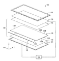
- FIG. 1 is an exploded perspective view showing a schematic configuration of a liquid crystal display device 100 according to the present embodiment.
- the liquid crystal display device 100 includes a bezel 102, a chassis 101, a reflection sheet 110, a light guide member 130, a laminated sheet group 150, a liquid crystal display panel 170, a light source group 103, and a control unit 160.
- a reflective sheet 110, a light guide member 130, a laminated sheet group 150, and a liquid crystal display panel 170 are arranged in this order from the bottom (chassis 101 side).
- a light source group 103 is disposed on the side of the light guide plate member 130. The light source group 103 and the liquid crystal display panel 170 are connected to the control unit 160.
- the backlight 120 includes a reflection sheet 110, a light guide member 130, a laminated sheet group 150, and a light source group 130.
- the light guide member 130 has a substantially flat plate shape.
- the light source group 103 is disposed on one side of the light guide member 130 in the short direction, and includes a plurality of LEDs (Light Emitting Diodes) as light sources. These LEDs are mounted on a circuit board at intervals.
- LEDs Light Emitting Diodes
- the light source group 103 is disposed only on one side of the light guide member 130 in the short direction.
- the light source group 103 may also be disposed on the other side of the light guide member 130 in the short direction. That is, the light source group 103 may be disposed on both sides of the light guide member 130 in the lateral direction, or may be disposed on only one side.
- the light source group 103 may be arranged on one side or both sides of the light guide member 130 in the longitudinal direction.
- the light guide member 130 has an incident surface 130A (first end surface) at a position facing the plurality of LEDs.
- the light emitted from the LEDs of the light source group 103 enters the incident surface 130 ⁇ / b> A of the light guide member 130.
- the light guide member 130 has an exit surface 130B adjacent to the entrance surface 130A.
- the exit surface 130B is located at the top surface when the entrance surface 130A is the side surface of the light guide member 130.
- the direction from the incident surface 130A (first end surface) to the side surface 130F (second end surface) is defined as an x direction (first direction).
- the normal direction of the light guide member 130 is the z direction.
- a direction perpendicular to both the x direction and the z direction is defined as a y direction (second direction).
- the x direction can be a “light guide direction”.
- This “light guide direction” can be said to be the optical axis direction of the emitted light of the LEDs provided in the light source group 103.
- the z direction is a normal direction of the emission surface 130B.
- the light guide member 130 has a main surface 130C (back surface) facing away from the emission surface 130B.
- the light guide member 130 has a side surface 130D and a side surface 130E adjacent to the emission surface 130A and the main surface 130C.
- the side surface 130D and the side surface 130E face each other.
- a light diffusion structure 104 to be described later is formed on at least one of the main surface 130C and the emission surface 130B.
- the light incident from the incident surface 130A is guided toward the side surface 130F (second end surface) opposite to the incident surface 130A. Specifically, the light incident from the incident surface 130A propagates inward of the light guide member 130 while being totally reflected between the output surface 130B and the main surface 130C and between the side surface 130D and the side surface 130E. Then, the total reflection condition is broken mainly at the emission surface 130B, and the light is emitted.
- the light sources constituting the light source group 103 are not limited to LEDs, and fluorescent tubes and other light sources can be employed.
- the reflection sheet 110 is made of polyester, for example. More specifically, it is made of foamed PET (Polyethylene-Terephthalate) and has light reflection characteristics.
- the reflection sheet 110 has a function of reflecting light leaking from the main surface 130 ⁇ / b> C of the light guide member 130 and returning it to the light guide member 130.
- the laminated sheet group 150 includes a diffusion sheet and a plurality of prism sheets.
- the laminated sheet group 150 has a function of suppressing luminance unevenness of light emitted from the light guide member 130 and condensing the light from the light guide member 130 and emitting it toward the liquid crystal display panel 170.
- the liquid crystal display panel 170 includes an active matrix substrate, a color filter, a counter substrate, and a liquid crystal sealed between the active matrix substrate and the counter substrate. A plurality of thin film transistors (TFT) elements are formed on the active matrix substrate.
- TFT thin film transistors
- the liquid crystal display panel 170 has a function of receiving light emitted from the laminated sheet group 150 and displaying an image.
- the control unit 160 switches ON / OFF of each TFT element of the liquid crystal display panel 170 based on the image data to be displayed.
- the control unit 160 applies a video signal to the liquid crystal display panel 170, and sequentially turns off each of the plurality of LEDs in synchronization with the application timing.
- the bezel 102 has a window portion that allows the display area of the liquid crystal display panel 170 to be visible.
- FIG. 2 is a schematic diagram showing a schematic configuration of the light diffusion structure 104 including a plurality of light diffusion portions 104 ⁇ / b> A formed on the light guide member 130.
- the density state of the plurality of light diffusing portions 104 constituting the light diffusing structure 104 is emphasized.
- a light diffusion structure 104 including a plurality of light diffusion portions 104A is formed on the main surface 130C.
- the plurality of light diffusing portions 104A constituting the light diffusing structure 104 are spaced apart from each other at regular intervals and formed in a dot shape.
- the “interval” means an interval between centers in the light diffusion portions 104A adjacent to each other, and can also be referred to as “pitch”.
- the density of the light diffusing portion 104A in the light diffusing structure 104 is the dot diameter or the interval between dots (the distance between the centers of adjacent dots) when printing dots. ), Or by adjusting both the dot diameter and the dot interval.
- the density of the light diffusing structure 104 is “dense” as the dot diameter is larger and the interval between the dots is smaller.
- the density of the light diffusion structure 104 becomes “sparse” in the light diffusion structure.
- FIGS. 3A and 3B are plan views showing the arrangement of the light diffusion portions 104A (dots).
- the light diffusion portions 104A may be arranged in a square lattice pattern.
- they may be arranged in a hexagonal lattice shape.
- various arrangements can be applied as the arrangement of the light diffusion unit 104A.
- dot interval The distance between the centers of the adjacent light diffusion portions 104A (dots) (hereinafter referred to as dot interval) p is expressed by the following formula (1), where t is the thickness of the light guide member 130. p ⁇ 2.5t / 3 Formula (1) It is desirable to satisfy. By arranging the dots at a pattern pitch that satisfies the above formula (1), it is possible to prevent the dots from being visually recognized. For this reason, the light source module excellent in screen quality is realizable.
- the dot interval p is the length of the diagonal of the square lattice and the distance of two square lattices, and is not constant.
- the maximum value p max of the dot interval p may be applied to the above equation (1). That is, when the dot interval p is not constant, when the maximum value of the dot interval of the light diffusing portion 104A is p max and the thickness of the light guide member 130 is t, p max is expressed by the following formula (1 ′), p max ⁇ 2.5t / 3 Formula (1 ′) Should be satisfied.
- the inventors of the present application have not only the size of the luminance unevenness but also the luminance unevenness as a main factor that causes the luminance unevenness to be visually recognized. Clarified the degree of change (gradient of luminance distribution). Based on this result, it was derived that, as a condition that the luminance unevenness is not visually recognized (not visually recognized), if the inclination of the luminance distribution in the luminance unevenness is 1.0% / mm or less, it is difficult to be visually recognized as the luminance unevenness.
- each light diffusion portion 104A (dot) is regarded as a light source that emits light (scatters)
- the light diffusion structure 104 is considered to be an aggregate of light sources arranged at a dot interval (pitch) p. Can do. If these light sources (light diffusing portions 104A) are separated by t (thickness of the light guide member 130), a relatively uniform luminance distribution (luminance unevenness of 1.0% / mm or less) is realized.
- the light diffusing portion 104A (dot) is not visually observed. As a result, it is possible to improve the screen quality.
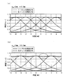
- FIG. 4 is a graph showing the relationship between the maximum value (p max ) of the dot interval and the luminance distribution.
- FIG. 4A shows a case where the maximum value (p max ) of the dot interval is 2 mm and the thickness t of the light guide member 130 is 3.0 mm.
- the luminance distribution of each dot is indicated by a dotted line
- the total luminance distribution obtained by adding the luminance distributions of each dot is indicated by a solid line. Note that the total luminance distribution can be said to be a luminance distribution when light scattered by the light diffusion structure 104 inside the light guide member 130 is emitted from the emission surface 130B.
- the total luminance distribution indicated by the solid line is substantially flat. Distribution.
- the maximum value of the dot interval (p max ) 3 mm and the thickness t of the light guide member 130 is 3.0 mm
- the total luminance distribution has 5 % Uneven brightness appears.
- the luminance unevenness shown in FIG. 4B is 3.3% / mm when converted to the inclination of the luminance distribution, and is a visually recognized luminance unevenness. Further, since this luminance unevenness exists corresponding to the luminance distribution (dotted line distribution) of each dot, it means that the dot is visually recognized.
- FIG. 4A and 4B and FIG. 5 are graphs when the thickness t of the light guide member 130 is 3.0 mm. Even when the thickness t of the light guide member 130 is changed, the relationship between the thickness t of the light guide member 130 and the dot interval p is similar.
- the inventors of the present application derived the equation m (1 ′) from the relationship between the dot interval p and the luminance unevenness described above. Therefore, by setting the maximum value (p max ) of the dot interval so as to satisfy the above formula (1 ′), it is possible to suppress the dots from being visually recognized and improve the screen quality. Similarly, when the dot interval p is constant, it is obvious that the same effect can be obtained by setting the dot interval p so as to satisfy the above formula (1).
- the density per unit area (unit cell) of dots arranged to satisfy the above formula (1) is between 0.4% / unit and 67% / unit (0.4% / unit or more, 67% / unit).
- the distance between dots can be set to 0.1 mm or more. For this reason, for example, when the light diffusing portion 104A (dots) is formed by a method such as screen printing, the dots do not adhere to each other due to the influence of blurring or rubbing. For this reason, yield, screen quality, optical characteristics and the like are improved.
- the density per unit area of the dots is larger than 67% / unit, it becomes easy to be absorbed by the material constituting the light diffusion portion 103A, and a large color change occurs. For this reason, in the light diffusion portion 103A, a portion having a high density and a portion having a low density are generated, and color unevenness occurs.
- the density per unit area of the dots is 0.4% / unit or more, it is possible to suppress the dot diameter from becoming too small. For this reason, it becomes easy to form the light diffusion portions 104A (dots) by a method such as screen printing.
- the unit area (unit) is intended to be an area in a range surrounded by the minimum pitch in FIG.
- the unit area is a square area with one side having a half length of p max .
- the area is an equilateral triangle having p as one side.
- the light diffusion structure 104 is formed on the main surface 130C of the light guide member 130.
- the light diffusion structure 104 may be formed on either the main surface 130C or the emission surface 130B. It may be provided on both the surface 130C and the exit surface 130B.
- the light diffusion structure 104 is formed on the exit surface 130B side, even if the maximum value of the dot interval (p max ) satisfies the above formula (1), the light diffusion structure 104 is directly above the backlight 120. The distance to the part is closer. Therefore, the plurality of diffusion portions 104 ⁇ / b> A (dots) constituting the light diffusion structure 104 may be visually observed through the liquid crystal panel 170. Therefore, it is preferable that the light diffusion structure 104 is formed on the main surface 130 ⁇ / b> C facing the emission surface 130 ⁇ / b> B rather than the emission surface 130 ⁇ / b> B of the light guide member 130.
- the light diffusion portion 104A is formed, for example, by dispersing light scattering fine particles in a polymer and then screen-printing the polymer on the main surface 130C.
- a phosphor may be used as the light scattering particles.
- the light diffusion portion 104A may be configured by forming a fine uneven shape such as a prism on the main surface 130C.
- the light diffusing portion 104A may be configured by performing blasting on the main surface 103C.
- the light diffusion portion 104A formed on the main surface 130C has a function of changing the optical path of light propagating through the light guide member 130. Specifically, the light propagating through the light guide member 130 is diffused by entering the light diffusion portion 104A of the main surface 130C, and the direction of traveling through the light guide member 130 is changed. As a result, at least a part of the light diffused by the light diffusion unit 104A is emitted from the emission surface 130B to the outside without being totally reflected by the emission surface 130B.
- the luminance distribution of the emitted light can be controlled depending on the position and density of the light diffusion portion 130A on the main surface 130C of the light guide member 130. it can. That is, the luminance distribution of the emitted light from the light guide member 130A is controlled by the density distribution of the light diffusion structure 104 formed on the main surface 130A.
- the density distribution (printing pattern) of the light diffusion portion 104A in the light diffusion structure 104 which is a feature of the backlight of the present embodiment, will be described.
- FIG. 6 shows the dot diameter distribution of the light diffusion portion 104A formed on the light guide member 130
- FIG. 6A shows the dot diameter distribution viewed from the z direction
- FIG. 6B shows the dot diameter distribution in FIG. 6 is a graph showing a dot diameter distribution in a DD ′ line cross section (vertical cross section in the center of the screen) in a)
- FIGS. 6C to 6E are respectively AA ′ lines in FIG. 6A.
- 6 is a graph showing dot diameter distributions in a cross section, a cross section along line BB ′, and a cross section along line CC ′ (both are cross sections of the screen).
- 6A to 6E show the size of the light guide member 130 used in the 60-type liquid crystal display device (for example, a size of about 1330 mm ⁇ 765 mm) as the size of the light guide member 130. Yes.
- the light diffusing structure 104 composed of a plurality of light diffusing portions 104A has a structure formed in a dot shape at regular intervals. Accordingly, the dot diameter distributions shown in FIGS. 6A to 6E are the same as the density distribution of the light diffusion structure 104 more specifically. Therefore, in the following description, it will be described not as a distribution of dot diameters but as a density distribution of the light diffusion structure 104.
- the density distribution of the light diffusion structure 104 is two-dimensionally represented.
- the density is shown by shading.
- a dark color portion is a low density portion
- a light color portion is a high density portion.
- the density is also shown by contour lines for easy understanding.
- the light diffusion structure 104 moves from the incident surface 130A side toward the light guide direction (side surface 130F side). , Formed so as to increase the density.
- Light entering the light guide member 130 from the incident surface 130A is diffused and the luminance is attenuated as the distance from the incident surface 130A increases. Therefore, as described above, by increasing the dot diameter of the light diffusion portion 104A as the distance from the incident surface 130A increases, it is possible to suppress the variation in the luminance of the light emitted from the emission surface 130B.
- by increasing the density of the light diffusion structure 104 as the distance from the incident surface 130A increases it is possible to suppress the occurrence of variations in the luminance of light emitted from the emission surface 130B.
- the density distribution of the light diffusion structure 104 decreases near the surface (side surface 130F) facing the light incident surface 130A. This is a result of designing in consideration of the reflected light from the surface facing the incident surface 130A. In the vicinity of the surface facing the incident surface 130A, light is guided from the incident surface 130A side, and light is reflected from the facing surface (side surface 130F). The reflected light is scattered by the light diffusion structure 104 and emitted from the emission surface 140B. Therefore, the density distribution of the light diffusing structure 104 is set so that the density decreases in the vicinity of the surface facing the incident surface 130A.
- the light not extracted by the light diffusion structure 104 is incident on the incident surface 130A. Is emitted from the surface (side surface 130F) facing the surface. Therefore, it is preferable that a reflective member or the like is provided on the facing surface (side surface 130F). Thereby, radiation of light from the side surface 130F can be prevented and light can be reflected again from the side surface 130F into the light guide member 130. As a result, the light utilization efficiency can be improved by recombining the reflected light.
- the dot diameter of the light diffusing portion 104A is in the direction parallel to the light guide direction (DD ′ line direction). It is formed so that the density becomes maximum in the vicinity of the central portion of 130. That is, the density of the light diffusing structure 104 increases near the center of the light guide member 130. Thereby, it is possible to suppress the occurrence of variations in luminance of light emitted from the emission surface 130B.
- the density of the light diffusion structure 104 in the direction perpendicular to the light guide direction is formed to have a distribution having three or more extreme values.
- the “extreme value” here is a value when the density distribution of the light diffusing structure 104 is approximated as a function of a curve, and the slope of the tangent becomes zero, and includes “maximum value” and “minimum value”. To do.
- the positions indicated by “arrows” in FIGS. 6C to 6E correspond to the minimum value.
- the density distribution of the light diffusion structure 104 has a maximum value at the center in the AA ′ section, the BB ′ section, and the CC ′ section. It is desirable to have. This is due to the following reason. That is, the luminance distribution of the backlight is required to increase the luminance of the central portion in the y direction and smoothly decrease the luminance of the peripheral portion in order to reduce power consumption and improve screen quality. It is. Therefore, it is necessary to increase the density of the light diffusing structure 104 at the center of the light guide member 130 in the y direction.
- the density distribution of the light diffusing structure 104 has a minimum value in a region from 300 to 440 mm from both end surfaces in the y direction (side surfaces 130D and 130E shown in FIGS. 1 and 2) of the light guide member 130.
- the y direction The density increases toward the end face of.
- the degree of increase in the density of the light diffusion structure 104 (rate of change in density before and after the minimum value) changes in the x direction, and the light guide member 130 has a central portion in the light guide direction (BB ′ line).
- a maximum value exists between the surface (side surface 130F) facing the incident surface 130A.
- the dimension of the light source group 103 is preferably smaller than the dimension of the light guide member 130 in the width direction (A-A ′ line direction in FIG. 6A; y direction).
- the dimension of the light source group 103 is larger than the dimension of the light guide member 130 in the width direction, light that does not optically couple to the light guide member 130 (does not enter the incident surface 130A) exists in the incident light from the light source group 103. To do. For this reason, the light utilization efficiency deteriorates, which is not preferable. Further, light that is not optically coupled to the light guide member 130 becomes stray light and is reflected by the chassis 101 shown in FIG.
- the size of the light source group 103 is preferably smaller than the size of the light guide member 130 in the width direction.
- the luminance distribution of the backlight is required to have a high luminance in the central portion (in the y direction) and a smooth decrease in luminance in the peripheral portion. .
- the light diffusion structure 104 is designed so as to have a density distribution with a large central part (in the y direction) and a small peripheral part.
- the density distribution of the light diffusing structure 104 is simply a distribution with a small peripheral part, it is affected by the light amount difference in the both ends of the incident surface 130A in the y direction, and a smooth luminance distribution such as a Gaussian distribution or a quadratic function is obtained. It becomes difficult to realize. Therefore, in the backlight of the present embodiment, in order to correct this light amount difference, the density distribution of the light diffusion structure 104 is the end of the light guide member 130 in the y direction in the direction perpendicular to the light guide direction (y direction).
- the light source group 103 that couples light to the light guide member 130 a light source group in which LEDs (Light Emitting Diodes) are mounted on a circuit board at intervals is used. If the LEDs constituting the light source group 103 have variations in luminance, the luminance unevenness also appears in the light emitted from the light guide member 130 (light emitted from the emission surface 130B) corresponding to the variation in luminance of the LEDs. .
- LEDs Light Emitting Diodes
- a part of the light scattered by the light diffusing structure 104 is guided in the light guide member 130 and emitted from the end faces parallel to the light guide direction (side surfaces 130D and 130E of the light guide member 130 shown in FIGS. 1 and 2). Will do. Further, the light emitted from the light source group 103 spreads in the plane of the light guide member 130 and is guided. Thereby, the light quantity which guides the y direction edge part of the light guide member 130 becomes relatively low in the vicinity of the surface (side surface 130F shown in FIGS. 1 and 2) facing the incident surface 130A, and the y direction center portion. The difference in the amount of light becomes relatively large.
- the density distribution of the light diffusing structure 104 is minimized near the end in the y direction of the light guide member 130 in the direction perpendicular to the light guide direction (y direction). It is effective to increase the density from the position in the y direction corresponding to the minimum value toward the end in the y direction. As described above, this is an effective configuration even when the size of the light source group 103 is smaller than the size of the light guide member 130 in the width direction or when the light source 103A forming the light source group 103 has a distribution.
- the inventors of the present application have determined that the dimension of the light guide member 130 in the direction perpendicular to the light guide direction (y direction) is H, and the density of the light diffusion structure 104 Since the minimum value of the distribution is in the region from both ends of the light guide member 130 in the direction perpendicular to the light guide direction to H / 3, a smooth luminance distribution such as a quadratic curve or a Gaussian distribution can be realized. Was revealed.
- the amount of light that guides the vicinity of the end portion in the y direction of the light guide member 130 is the surface facing the incident surface 130A (see FIG. 1 and 2 are relatively low in the vicinity of the side surface 130F), and the light amount difference from the central portion in the y direction is relatively large.
- the amount of light guided near the end in the y direction of the light guide member 130 decreases in the order of the CC ′ section, the BB ′ section, and the AA ′ section.
- the light amount difference from the central portion also increases in this order.
- the degree to which the density of the light diffusing structure 104 increases is measured on the surface facing the incident surface 130A (the side surface 130F shown in FIGS. 1 and 2). It becomes relatively large in the near part.
- the difference in the amount of light between the vicinity of the end portion in the y direction and the central portion in the y direction in the vicinity of the side surface 130F is alleviated, and accordingly, the change rate of the density around the minimum value also becomes gentle.
- the density change rate around the minimum value changes in the x direction, and the central portion of the light guide member 130 in the light guide direction (B shown in FIG. 6A). It is preferable that a maximum value exists between the ⁇ B ′ line and a surface (side surface 130F shown in FIG. 6A) facing the incident surface 130A.
- the density of the light diffusion structure 104 in the direction perpendicular to the light guide direction is set to the above-described density distribution, it is possible to suppress a decrease in the amount of light extracted from both ends of the light guide member 130. Screen quality can be maintained.
- such a density distribution of the light diffusion structure 104 has an advantage when the light diffusion portion 104A is formed by a method such as screen printing.
- the printing direction is generally the direction perpendicular to the light guide direction in the light guide member 130 (y direction).
- the light diffusing portion 104A has a relatively small dimension of several micrometers to several tens of micrometers at the beginning and end of sliding due to printing rubbing or the like. Become. That is, the density of the light diffusion structure 104 is smaller than the design value at the sliding start portion and the sliding end portion (both ends in the y direction) of the light guide member 130. Accordingly, the amount of light extracted from both ends of the light guide member 130 in the y direction may decrease, and the luminance may decrease.
- the printing direction should be perpendicular to the light guide direction. Therefore, the density of the light diffusion structures 104 at both ends in the direction perpendicular to the light guide direction (AA ′ line direction, BB ′ line direction, CC ′ line direction) tends to be relatively small. It is in. Accordingly, the amount of light extracted from both ends of the light guide member 130 is reduced, and the luminance is reduced. Such a decrease in luminance is undesirable because it degrades the screen quality of the liquid crystal display device 100.
- the dot diameter of the light diffusion portion 104A is formed so as to increase toward both ends of the light guide member 130 in the direction (y direction) perpendicular to the light guide direction (FIG. 6A). ) To (e)).
- the size of the diffusing portion 104A at the beginning of sliding and the end of sliding is reduced by several micrometers to several tens of micrometers, compared with the case where the dot diameter is set smaller. The effect of error with the value is reduced. For this reason, it can suppress that the light quantity taken out from the both ends of the light guide member 130 falls, and can maintain favorable screen quality.
- the density distribution (dot diameter distribution) of the light diffusing structure 104 is the both ends of the light guide member 130 in the y direction (side surfaces 130D and 130E).
- the dot diameter is smaller in the vicinity.
- the dot diameter distribution in the A-A ′ section has a larger dot diameter as a whole compared to the dot diameter distribution in the C-C ′ section or the like. For this reason, even when the dimension of the diffusion portion 104A is reduced by several micrometers to several tens of micrometers, the influence of the error from the design value is smaller than that of the C-C ′ section.
- the effect of rubbing by screen printing is greater as it is closer to the incident surface 130A.
- the dot diameter of the light diffusing portion 104A is formed so as to increase toward both ends of the light guide member 130. This contributes to the suppression of the luminance reduction and the improvement of the screen quality.
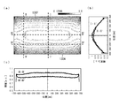
- FIGS. 8A to 8C show the results of analyzing the luminance distribution of the backlight using the light guide member 130 having the density distribution of the light diffusion structure 104 shown in FIGS. 6A to 6E.
- 9A to 9C show, as a comparative example, the luminance distribution of the backlight using the light guide member 201 in which the density of the light diffusion structure 204 shown in FIG. 10 is constant in the direction perpendicular to the light guide direction. The analysis result is shown.
- FIG. 8 and FIG. 9 is a plan view showing the luminance distribution two-dimensionally, and the level of luminance is expressed by shading.
- a darker color portion is a lower luminance portion, and a lighter color portion is a higher luminance portion.
- FIG. 8A and FIG. 9A show the brightness level of contour lines.
- FIG. 8 and FIG. 9B are graphs showing the luminance distribution in the longitudinal I-I ′ section and the II-II ′ section in FIG. 8 and FIG.
- FIG. 7 and FIG. 8C are graphs showing the luminance distribution in the horizontal III-III ′ section and the IV-IV ′ section in FIG. 8 and FIG. 8 and 9, the vertical axis in the graphs of (b) and (c) represents the relative value of the luminance, and the horizontal axis represents the center of the luminance distribution shown in (a) of FIGS. 8 and 9 as the origin. The position in the light guide member is shown.
- the backlight having the light guide member 130 having the density distribution of the light diffusion structure 104 shown in FIGS. 6A to 6E has contour lines with elliptical luminance distribution. It has become. From FIG. 8 (a), it can be seen that the luminance smoothly decreases from the center of the screen. This is apparent from the graphs of FIGS. 8B and 8C. As shown in FIGS. 8B and 8C, the II ′ and II-II ′ sections parallel to the light guide direction, and the III-III ′ section and IV-IV ′ perpendicular to the light guide direction. In all cross sections, the luminance distribution is symmetric with respect to the origin. Therefore, a smooth luminance distribution can be realized.
- the density of the light diffusion structure 204 is constant in the direction perpendicular to the light guide direction), as shown in FIG. There are no beautiful oval contours.
- the luminance distribution in the II ′ section (vertical section in the center of the screen) is symmetric with respect to the origin, and is a distribution that is smoothly reduced from the relative luminance at the origin. It has become.
- the luminance distribution in the II-II ′ section (vertical section at the horizontal end of the screen) is not symmetrical with respect to the origin, and the upper part of the screen is slightly darker than the lower part of the screen.
- the luminance distribution in the section III-III ′ is a distribution in which the luminance decreases from the center (origin) to the screen edge. It has become. However, in the vicinity of the edge of the screen, the luminance does not decrease so much. Further, the luminance distribution in the IV-IV ′ cross section (the horizontal cross section at the lower end of the screen) is a distribution in which the luminance is increased at the end of the screen.
- the luminance distribution is not smooth, and the luminance distribution has a wavy shape in some places. Become. Such a luminance distribution is visually recognized as luminance unevenness, and the screen quality is deteriorated.
- the backlight in this embodiment is superior in screen quality. Is obvious.
- the light source module (backlight) in the present embodiment provides three or more extreme values in the density distribution of the light diffusion structure in the direction perpendicular to the light guide direction as described above. Even when a large light guide member is used, the luminance at the center of the screen can be increased and the luminance distribution can be smoothly realized toward the edge of the screen. Therefore, it is possible to improve the screen quality and realize a light source module having excellent power consumption and optical characteristics.
- the dot interval of the light diffusion portion in the light source module of the present invention is an interval at which dots are not visually recognized, there is an effect that a light source module excellent in screen quality and optical characteristics can be realized.
- the diffusion portion (dot pattern) formed in the light source module of the present invention has a gap that can be easily printed. Therefore, when the dots are formed by a method such as screen printing, the dots do not stick together due to the influence of bleeding and rubbing, and the yield, screen quality, optical characteristics, and the like are improved.
- an electronic device of the present invention includes the light source module described above.
- an electronic device such as a light source module capable of obtaining uniform luminance display and a liquid crystal display device with excellent screen quality.
- the present invention can be used for backlights of liquid crystal display devices such as televisions and monitors, and is particularly applicable to side edge type backlights.
- Liquid crystal display device (electronic equipment) DESCRIPTION OF SYMBOLS 101 Chassis 102 Bezel 103 Light source group 104 Light diffusion structure 104A Light diffusion part 120 Backlight (light source module) 130 Light guide member 130A Incident surface (first end surface) 130B Outgoing surface 130C Main surface (back) 130D Side surface 130E Side surface 130F Side surface (second end surface) 150 Laminated Sheet Group 160 Control Unit 170 Liquid Crystal Display Panel
Landscapes
- Physics & Mathematics (AREA)
- General Physics & Mathematics (AREA)
- Optics & Photonics (AREA)
- Planar Illumination Modules (AREA)
- Liquid Crystal (AREA)
Abstract
L'invention porte sur un module de source de lumière, lequel module produit une distribution de luminosité dans laquelle la luminosité d'une partie centrale est élevée et la luminosité diminue selon une courbe à partir de la partie centrale vers les parties périphériques, et produit ainsi une excellente qualité d'image. La distribution de diamètre de points de la structure de lumière à dispersion a au moins trois valeurs extrêmes dans les directions de la ligne A-A', de la ligne B-B' et de la ligne C-C'.
Applications Claiming Priority (2)
| Application Number | Priority Date | Filing Date | Title |
|---|---|---|---|
| JP2011-258315 | 2011-11-25 | ||
| JP2011258315A JP5851217B2 (ja) | 2011-11-25 | 2011-11-25 | 光源モジュール、並びにそれを備えた電子機器および液晶表示装置 |
Publications (1)
| Publication Number | Publication Date |
|---|---|
| WO2013077237A1 true WO2013077237A1 (fr) | 2013-05-30 |
Family
ID=48469684
Family Applications (1)
| Application Number | Title | Priority Date | Filing Date |
|---|---|---|---|
| PCT/JP2012/079593 Ceased WO2013077237A1 (fr) | 2011-11-25 | 2012-11-15 | Module de source de lumière, dispositif électronique le comportant et dispositif d'affichage à cristaux liquides |
Country Status (2)
| Country | Link |
|---|---|
| JP (1) | JP5851217B2 (fr) |
| WO (1) | WO2013077237A1 (fr) |
Cited By (1)
| Publication number | Priority date | Publication date | Assignee | Title |
|---|---|---|---|---|
| ITTV20130101A1 (it) * | 2013-06-21 | 2014-12-22 | Monica Mazzoli | "dispositivo illuminante e decorativo a pannello, del tipo edge - lit" |
Families Citing this family (2)
| Publication number | Priority date | Publication date | Assignee | Title |
|---|---|---|---|---|
| JP6129694B2 (ja) * | 2013-09-04 | 2017-05-17 | 富士フイルム株式会社 | 光音響計測用プローブおよびそれを備えた光音響計測装置 |
| JP7043727B2 (ja) * | 2017-01-31 | 2022-03-30 | 大日本印刷株式会社 | 光波長変換シートの劣化評価方法、光波長変換シート、バックライト装置、および画像表示装置 |
Citations (5)
| Publication number | Priority date | Publication date | Assignee | Title |
|---|---|---|---|---|
| JPH0440268U (fr) * | 1990-08-02 | 1992-04-06 | ||
| JPH04162002A (ja) * | 1990-10-25 | 1992-06-05 | Mitsubishi Rayon Co Ltd | エッジライト方式面光源装置 |
| JP2000321993A (ja) * | 1999-05-11 | 2000-11-24 | Matsushita Electric Ind Co Ltd | 表示パネルとその製造方法、表示方法とそれを用いた表示装置とそれを搭載したデジタルカメラおよびビューファインダ、および画像処理方法 |
| JP2002343122A (ja) * | 2001-05-18 | 2002-11-29 | Kyocera Corp | 照明パネル、液晶表示装置および携帯端末または表示機器 |
| JP2009266819A (ja) * | 2008-04-24 | 2009-11-12 | Samsung Electronics Co Ltd | バックライトアッセンブリ |
Family Cites Families (3)
| Publication number | Priority date | Publication date | Assignee | Title |
|---|---|---|---|---|
| JP2004145035A (ja) * | 2002-10-25 | 2004-05-20 | Sanyo Electric Co Ltd | 面光源装置及びこれに用いる導光板の製造方法 |
| JP2008269866A (ja) * | 2007-04-18 | 2008-11-06 | Seiko Epson Corp | 照明装置及び液晶表示装置並びに電子機器 |
| BRPI1001233A2 (pt) * | 2009-10-07 | 2016-02-10 | Sharp Kk | "módulo de fonte de luz e aparelho eletrônico que inclui o mesmo" |
-
2011
- 2011-11-25 JP JP2011258315A patent/JP5851217B2/ja active Active
-
2012
- 2012-11-15 WO PCT/JP2012/079593 patent/WO2013077237A1/fr not_active Ceased
Patent Citations (5)
| Publication number | Priority date | Publication date | Assignee | Title |
|---|---|---|---|---|
| JPH0440268U (fr) * | 1990-08-02 | 1992-04-06 | ||
| JPH04162002A (ja) * | 1990-10-25 | 1992-06-05 | Mitsubishi Rayon Co Ltd | エッジライト方式面光源装置 |
| JP2000321993A (ja) * | 1999-05-11 | 2000-11-24 | Matsushita Electric Ind Co Ltd | 表示パネルとその製造方法、表示方法とそれを用いた表示装置とそれを搭載したデジタルカメラおよびビューファインダ、および画像処理方法 |
| JP2002343122A (ja) * | 2001-05-18 | 2002-11-29 | Kyocera Corp | 照明パネル、液晶表示装置および携帯端末または表示機器 |
| JP2009266819A (ja) * | 2008-04-24 | 2009-11-12 | Samsung Electronics Co Ltd | バックライトアッセンブリ |
Cited By (1)
| Publication number | Priority date | Publication date | Assignee | Title |
|---|---|---|---|---|
| ITTV20130101A1 (it) * | 2013-06-21 | 2014-12-22 | Monica Mazzoli | "dispositivo illuminante e decorativo a pannello, del tipo edge - lit" |
Also Published As
| Publication number | Publication date |
|---|---|
| JP5851217B2 (ja) | 2016-02-03 |
| JP2013114821A (ja) | 2013-06-10 |
Similar Documents
| Publication | Publication Date | Title |
|---|---|---|
| US8325295B2 (en) | Liquid crystal display device | |
| JP5021070B2 (ja) | 発光素子、照明装置および液晶表示装置 | |
| US8107036B2 (en) | Backlight device, liquid crystal display apparatus, and light deflecting sheet | |
| US7764334B2 (en) | Illumination apparatus comprising a light guide plate divided by wedge-shaped grooves having an apex angle of 15 degrees or less and a ratio of depth to thickness in a range of 0.4 to 0.7 | |
| US9651205B2 (en) | Lighting device with light shielding pattern and video display device using the same | |
| KR101508010B1 (ko) | 백라이트 조명 균일성 향상 시스템 | |
| CN104471306B (zh) | 照明装置和显示装置 | |
| WO2011129117A1 (fr) | Dispositif de rétroéclairage et appareil à afficheur à cristaux liquides | |
| US20100134722A1 (en) | Backlight module and display device using the same | |
| JP2009289701A (ja) | 照明装置、面光源装置、および液晶表示装置 | |
| JP2001133779A (ja) | 液晶表示装置 | |
| JP2012018880A (ja) | 面状照明装置、映像表示装置および光学シート | |
| CN102213385A (zh) | 图像显示装置以及用于该图像显示装置的背光装置 | |
| US7540630B2 (en) | Backlight module and scattering module for same | |
| US20120113682A1 (en) | Surface lighting apparatus | |
| US20130278866A1 (en) | Illumination device and liquid crystal display apparatus using the same | |
| JP5851217B2 (ja) | 光源モジュール、並びにそれを備えた電子機器および液晶表示装置 | |
| US20080043488A1 (en) | Backlight unit of a liquid crystal display device | |
| US20150247964A1 (en) | Light source device and display device equipped with same | |
| WO2019021952A1 (fr) | Dispositif d'éclairage et dispositif d'affichage | |
| JP5685099B2 (ja) | 面光源素子及びそれを備えた表示装置 | |
| US20140009965A1 (en) | Lighting device and display device | |
| JP2006134661A (ja) | 面状光源及びこれを用いた液晶表示装置 | |
| JP2022078407A (ja) | 照明装置及び表示装置 | |
| KR101096514B1 (ko) | 백라이트 어셈블리, 그것의 제조 방법, 이 백라이트 어셈블리를 포함하는 액정표시장치 |
Legal Events
| Date | Code | Title | Description |
|---|---|---|---|
| 121 | Ep: the epo has been informed by wipo that ep was designated in this application |
Ref document number: 12851350 Country of ref document: EP Kind code of ref document: A1 |
|
| NENP | Non-entry into the national phase |
Ref country code: DE |
|
| 122 | Ep: pct application non-entry in european phase |
Ref document number: 12851350 Country of ref document: EP Kind code of ref document: A1 |