WO2013077255A1 - Film de barrière vis-à-vis des gaz et dispositif électronique - Google Patents
Film de barrière vis-à-vis des gaz et dispositif électronique Download PDFInfo
- Publication number
- WO2013077255A1 WO2013077255A1 PCT/JP2012/079732 JP2012079732W WO2013077255A1 WO 2013077255 A1 WO2013077255 A1 WO 2013077255A1 JP 2012079732 W JP2012079732 W JP 2012079732W WO 2013077255 A1 WO2013077255 A1 WO 2013077255A1
- Authority
- WO
- WIPO (PCT)
- Prior art keywords
- gas barrier
- layer
- film
- barrier film
- group
- Prior art date
- Legal status (The legal status is an assumption and is not a legal conclusion. Google has not performed a legal analysis and makes no representation as to the accuracy of the status listed.)
- Ceased
Links
Images
Classifications
-
- C—CHEMISTRY; METALLURGY
- C08—ORGANIC MACROMOLECULAR COMPOUNDS; THEIR PREPARATION OR CHEMICAL WORKING-UP; COMPOSITIONS BASED THEREON
- C08J—WORKING-UP; GENERAL PROCESSES OF COMPOUNDING; AFTER-TREATMENT NOT COVERED BY SUBCLASSES C08B, C08C, C08F, C08G or C08H
- C08J7/00—Chemical treatment or coating of shaped articles made of macromolecular substances
- C08J7/04—Coating
- C08J7/048—Forming gas barrier coatings
-
- C—CHEMISTRY; METALLURGY
- C08—ORGANIC MACROMOLECULAR COMPOUNDS; THEIR PREPARATION OR CHEMICAL WORKING-UP; COMPOSITIONS BASED THEREON
- C08J—WORKING-UP; GENERAL PROCESSES OF COMPOUNDING; AFTER-TREATMENT NOT COVERED BY SUBCLASSES C08B, C08C, C08F, C08G or C08H
- C08J7/00—Chemical treatment or coating of shaped articles made of macromolecular substances
- C08J7/04—Coating
- C08J7/042—Coating with two or more layers, where at least one layer of a composition contains a polymer binder
-
- C—CHEMISTRY; METALLURGY
- C08—ORGANIC MACROMOLECULAR COMPOUNDS; THEIR PREPARATION OR CHEMICAL WORKING-UP; COMPOSITIONS BASED THEREON
- C08J—WORKING-UP; GENERAL PROCESSES OF COMPOUNDING; AFTER-TREATMENT NOT COVERED BY SUBCLASSES C08B, C08C, C08F, C08G or C08H
- C08J7/00—Chemical treatment or coating of shaped articles made of macromolecular substances
- C08J7/04—Coating
- C08J7/0427—Coating with only one layer of a composition containing a polymer binder
-
- C—CHEMISTRY; METALLURGY
- C08—ORGANIC MACROMOLECULAR COMPOUNDS; THEIR PREPARATION OR CHEMICAL WORKING-UP; COMPOSITIONS BASED THEREON
- C08J—WORKING-UP; GENERAL PROCESSES OF COMPOUNDING; AFTER-TREATMENT NOT COVERED BY SUBCLASSES C08B, C08C, C08F, C08G or C08H
- C08J7/00—Chemical treatment or coating of shaped articles made of macromolecular substances
- C08J7/04—Coating
- C08J7/043—Improving the adhesiveness of the coatings per se, e.g. forming primers
-
- H—ELECTRICITY
- H05—ELECTRIC TECHNIQUES NOT OTHERWISE PROVIDED FOR
- H05K—PRINTED CIRCUITS; CASINGS OR CONSTRUCTIONAL DETAILS OF ELECTRIC APPARATUS; MANUFACTURE OF ASSEMBLAGES OF ELECTRICAL COMPONENTS
- H05K5/00—Casings, cabinets or drawers for electric apparatus
- H05K5/06—Hermetically-sealed casings
- H05K5/069—Other details of the casing, e.g. wall structure, passage for a connector, a cable, a shaft
-
- C—CHEMISTRY; METALLURGY
- C08—ORGANIC MACROMOLECULAR COMPOUNDS; THEIR PREPARATION OR CHEMICAL WORKING-UP; COMPOSITIONS BASED THEREON
- C08J—WORKING-UP; GENERAL PROCESSES OF COMPOUNDING; AFTER-TREATMENT NOT COVERED BY SUBCLASSES C08B, C08C, C08F, C08G or C08H
- C08J2483/00—Characterised by the use of macromolecular compounds obtained by reactions forming in the main chain of the macromolecule a linkage containing silicon with or without sulfur, nitrogen, oxygen, or carbon only; Derivatives of such polymers
- C08J2483/16—Characterised by the use of macromolecular compounds obtained by reactions forming in the main chain of the macromolecule a linkage containing silicon with or without sulfur, nitrogen, oxygen, or carbon only; Derivatives of such polymers in which all the silicon atoms are connected by linkages other than oxygen atoms
-
- H—ELECTRICITY
- H10—SEMICONDUCTOR DEVICES; ELECTRIC SOLID-STATE DEVICES NOT OTHERWISE PROVIDED FOR
- H10K—ORGANIC ELECTRIC SOLID-STATE DEVICES
- H10K50/00—Organic light-emitting devices
- H10K50/80—Constructional details
- H10K50/84—Passivation; Containers; Encapsulations
- H10K50/842—Containers
- H10K50/8426—Peripheral sealing arrangements, e.g. adhesives, sealants
-
- H—ELECTRICITY
- H10—SEMICONDUCTOR DEVICES; ELECTRIC SOLID-STATE DEVICES NOT OTHERWISE PROVIDED FOR
- H10K—ORGANIC ELECTRIC SOLID-STATE DEVICES
- H10K50/00—Organic light-emitting devices
- H10K50/80—Constructional details
- H10K50/84—Passivation; Containers; Encapsulations
- H10K50/844—Encapsulations
-
- Y—GENERAL TAGGING OF NEW TECHNOLOGICAL DEVELOPMENTS; GENERAL TAGGING OF CROSS-SECTIONAL TECHNOLOGIES SPANNING OVER SEVERAL SECTIONS OF THE IPC; TECHNICAL SUBJECTS COVERED BY FORMER USPC CROSS-REFERENCE ART COLLECTIONS [XRACs] AND DIGESTS
- Y10—TECHNICAL SUBJECTS COVERED BY FORMER USPC
- Y10T—TECHNICAL SUBJECTS COVERED BY FORMER US CLASSIFICATION
- Y10T428/00—Stock material or miscellaneous articles
- Y10T428/23—Sheet including cover or casing
- Y10T428/239—Complete cover or casing
-
- Y—GENERAL TAGGING OF NEW TECHNOLOGICAL DEVELOPMENTS; GENERAL TAGGING OF CROSS-SECTIONAL TECHNOLOGIES SPANNING OVER SEVERAL SECTIONS OF THE IPC; TECHNICAL SUBJECTS COVERED BY FORMER USPC CROSS-REFERENCE ART COLLECTIONS [XRACs] AND DIGESTS
- Y10—TECHNICAL SUBJECTS COVERED BY FORMER USPC
- Y10T—TECHNICAL SUBJECTS COVERED BY FORMER US CLASSIFICATION
- Y10T428/00—Stock material or miscellaneous articles
- Y10T428/24—Structurally defined web or sheet [e.g., overall dimension, etc.]
- Y10T428/24355—Continuous and nonuniform or irregular surface on layer or component [e.g., roofing, etc.]
- Y10T428/24364—Continuous and nonuniform or irregular surface on layer or component [e.g., roofing, etc.] with transparent or protective coating
-
- Y—GENERAL TAGGING OF NEW TECHNOLOGICAL DEVELOPMENTS; GENERAL TAGGING OF CROSS-SECTIONAL TECHNOLOGIES SPANNING OVER SEVERAL SECTIONS OF THE IPC; TECHNICAL SUBJECTS COVERED BY FORMER USPC CROSS-REFERENCE ART COLLECTIONS [XRACs] AND DIGESTS
- Y10—TECHNICAL SUBJECTS COVERED BY FORMER USPC
- Y10T—TECHNICAL SUBJECTS COVERED BY FORMER US CLASSIFICATION
- Y10T428/00—Stock material or miscellaneous articles
- Y10T428/26—Web or sheet containing structurally defined element or component, the element or component having a specified physical dimension
- Y10T428/263—Coating layer not in excess of 5 mils thick or equivalent
- Y10T428/264—Up to 3 mils
- Y10T428/265—1 mil or less
Definitions
- the present invention relates to a gas barrier film and an electronic device using the gas barrier film.
- a gas barrier film formed by laminating a plurality of layers including a thin film of a metal oxide such as aluminum oxide, magnesium oxide, or silicon oxide on the surface of a plastic substrate or a resin film is used for various gases such as water vapor and oxygen. It is widely used in packaging applications for articles that require blocking, for example, packaging applications for preventing alteration of food, industrial products, pharmaceuticals, and the like.
- gas barrier films are required to be used for sealing electronic devices such as flexible solar cell elements, organic electroluminescence (EL) elements, and liquid crystal display elements. Is being studied. However, regarding the sealing of these electronic devices, a gas barrier film having a sufficient performance has not yet been obtained since a very high gas barrier property at the glass substrate level is required.
- a chemical deposition method in which an organic silicon compound typified by tetraethoxysilane (TEOS) is oxidized with oxygen plasma under reduced pressure while an inorganic film is formed on the substrate.
- TEOS tetraethoxysilane
- Gas phase methods such as Chemical Vapor Deposition) and physical deposition methods (vacuum evaporation method and sputtering method) of evaporating metal Si using a semiconductor laser and depositing an inorganic film on the substrate in the presence of oxygen are known. Yes.
- required for sealing of an electronic device is not obtained in the industrial level in which productivity is calculated
- studies such as simply increasing the film thickness of an inorganic film by a vapor phase method or laminating a plurality of inorganic films have been made, but defects may continuously grow or cracks may increase. The gas barrier property has not been improved.
- the inorganic film can be inorganic without continuously growing defects. While ensuring the total thickness of the film, further studies have been made to improve the gas barrier property by the so-called labyrinth effect in which the gas permeation path length is increased by the fact that the defect position in the surface of each inorganic film is different. .
- the gas barrier property is not sufficient, and the manufacturing process is complicated. For example, the productivity of the gas barrier film is extremely low, so that it is considered difficult to put it to practical use in terms of cost.
- Technical studies have been made to improve the gas barrier layer.
- studies have been made to develop high gas barrier properties by using polysilazane as an inorganic precursor compound.
- Polysilazane is a compound having a basic structure of — (SiH 2 —NH) — (for example, perhydropolysilazane). When polysilazane is subjected to heat treatment or wet heat treatment in an oxidizing atmosphere, it changes into silicon oxide via silicon oxynitride.
- VUV vacuum ultraviolet light
- a silicon oxynitride film or a silicon oxide film can be formed at a relatively low temperature by causing an oxidation reaction with active oxygen or ozone to proceed while being directly cut by the action of photons alone.
- Non-Patent Document 1 discloses a method for producing a gas barrier film by irradiating a polysilazane coating film with VUV light using an excimer lamp.
- the layer configuration and production conditions of the gas barrier film have not been studied in detail, and the gas barrier properties of the obtained gas barrier film are not as good as those required for electronic devices.
- Patent Document 1 discloses a method for producing a gas barrier film by irradiating a polysilazane coating film containing a basic catalyst with VUV light and UV light.
- a gas barrier film in which three layers of gas barrier layers formed by applying polysilazane on a resin substrate, drying and irradiating with VUV light are laminated.
- the barrier property is not as good as the gas barrier property required for electronic devices.
- a binder resin conventionally used in the production of a coating containing polysiloxane is mentioned, but it has a specific structure other than the catalyst. There is no suggestion of improving the gas barrier properties by adding an appropriate amount of a compound.
- two or more gas barrier layers are formed by irradiating a polysilazane coating film having a film thickness of 250 nm or less on a resin substrate having a smooth surface (surface Ra value of less than 12 nm) with VUV light.
- An improved gas barrier film is disclosed. And, by making the polysilazane coating thin, it suppresses the generation of cracks during irradiation with VUV light, and attempts to improve the gas barrier property by increasing the thickness by laminating this, but laminating the thin layer Even in this case, if the total thickness of the gas barrier layer exceeds a certain value, cracks are generated, so that the gas barrier property required for the electronic device cannot be obtained.
- a resin base material having a smooth surface is easily damaged when transported, and is a technique with poor productivity including yield.
- Patent Document 3 discloses a gas barrier film having a thermosetting silicon-containing organic-inorganic composite copolymer film in which polysilazane and a polysiloxane polymer are mixed.
- this organic-inorganic composite copolymer film has substantially no gas barrier property, and has a function of improving adhesion with the gas barrier inorganic oxide layer formed thereon and an inorganic oxide by stress relaxation. It is a film
- the present invention has been made in view of the above problems, and an object thereof is to provide a gas barrier film having high gas barrier performance and an electronic device using the same.
- a gas barrier film provided on a substrate with a gas barrier layer formed by subjecting a layer containing polysilazane to vacuum ultraviolet irradiation,
- the gas barrier layer contains the compound A satisfying all of the following (a), (b), and (c) in a range of 1% by mass to 40% by mass with respect to the entire gas barrier layer.
- a gas barrier film characterized by that. (A) It has an Si—O bond and an organic group directly bonded to Si. (B) It has a Si—H group or a Si—OH group. (C) The molecular weight is 90 or more and 1200 or less.
- the invention according to claim 2 is the gas barrier film according to claim 1,
- the compound A has a structure represented by the following general formula (1). (In the formula, R represents an organic group. X represents H or OH.)
- the invention according to claim 3 is the gas barrier film according to claim 1 or 2,
- the compound A has a cyclic structure or a cage structure composed of Si—O—Si bonds.
- the invention according to claim 4 is the gas barrier film according to any one of claims 1 to 3,
- the number of carbon atoms contained in the organic group is 6 or less.
- the invention according to claim 5 is the gas barrier film according to any one of claims 1 to 4,
- the organic group is any one of a methyl group, an ethyl group, and a phenyl group.
- the invention according to claim 6 is the gas barrier film according to any one of claims 1 to 5,
- the substrate has a surface roughness Rz of 200 nm or more and 500 nm or less.
- the invention according to claim 7 is the gas barrier film according to any one of claims 1 to 6, At least one intermediate layer is provided between the substrate and the gas barrier layer, and the surface roughness of the intermediate layer in contact with the gas barrier layer is 200 nm to 500 nm in Rz.
- the invention according to claim 8 is the gas barrier film according to any one of claims 1 to 7,
- the gas barrier layer has a thickness of at least 250 nm.
- the invention according to claim 9 is an electronic device, A gas barrier film according to any one of claims 1 to 8, and an electronic device sealed with the gas barrier film.
- the compound A satisfying all of the following (a), (b), and (c) is contained in the range of 1% by mass or more and 40% by mass or less with respect to the entire gas barrier layer, thereby being excellent in productivity. It has been found that a gas barrier film that can be manufactured by a coating method and has a high gas barrier performance required for sealing applications of electronic devices can be realized, and the present invention has been achieved.
- (A) It has an Si—O bond and an organic group directly bonded to Si.
- (B) It has a Si—H group or a Si—OH group.
- the molecular weight is 90 or more and 1200 or less.
- Increasing the energy of VUV light irradiation to the perhydropolysilazane coating generally improves the gas barrier properties of the film quality, but the coating shrinkage also increases and cracks tend to occur, so the gas barrier properties are substantially improved. Will hit the peak. Further, the flexibility is also lowered, and cracks are easily generated even when the film is bent. The ease of occurrence of this crack and the decrease in flexibility become more prominent as the perhydropolysilazane coating film becomes thicker. In addition, the number of thin layers of the perhydropolysilazane coating film is slightly improved in the ease of cracking with respect to the total film thickness.
- the gas barrier property of the gas barrier layer using the perhydropolysilazane coating film is greatly improved by a combination of simple methods that increase the irradiation energy of VUV light or increase the total film thickness of the coating film. I can't hope.
- a method of suppressing crack generation of the perhydropolysilazane coating mixing polysilazane having an organic resin or an organic group with perhydropolysilazane has been studied, but in an addition amount region where crack generation can be suppressed, Since the gas barrier property is greatly reduced, the problem has not been solved.
- the present inventor has mixed a compound having a specific structure and having a specific molecular weight range into a polysilazane coating film in an appropriate amount range, whereby a gas barrier property of a coating film to be a gas barrier layer. It has been found that both improvement and crack suppression can be achieved. It has also been found that since the coating film can be thickened, the gas barrier layer is less susceptible to the surface roughness of the substrate. As a result, a gas barrier film having high gas barrier properties and flexibility and good productivity could be obtained.
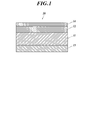
- the gas barrier film 10 includes at least one gas barrier layer 14 on a substrate 11 such as a resin film.
- This gas barrier layer 14 is a layer formed by subjecting a layer containing polysilazane to vacuum ultraviolet irradiation, and the gas barrier layer 14 contains a compound A that satisfies all of the following (a), (b), and (c): It is contained in the range of 1% by mass to 40% by mass with respect to the entire gas barrier layer.
- (A) It has an Si—O bond and an organic group directly bonded to Si.
- (B) It has a Si—H group or a Si—OH group.
- C The molecular weight is 90 or more and 1200 or less.
- the gas barrier film 10 includes a base material 11, an intermediate layer 12 formed on one surface of the base material 11, and a gas barrier layer laminated on the intermediate layer 12. 14 and a bleed-out prevention layer 13 formed on the other surface of the substrate 11.
- the structure provided with the gas barrier layer 14 on both surfaces of the base material 11 may be sufficient.
- the base material 11 in the gas barrier film 10 of the present invention is a flexible bendable resin base material.
- the substrate 11 is not particularly limited as long as it is a film-like substrate that can hold the gas barrier layer 14.
- Examples of the resin base material applicable to the base material 11 include acrylic acid ester, methacrylic acid ester, polyethylene terephthalate (PET), polybutylene terephthalate, polyethylene naphthalate (PEN), polycarbonate (PC), polyarylate, and polychlorination.
- Each resin such as vinyl (PVC), polyethylene (PE), polypropylene (PP), polystyrene (PS), nylon (Ny), aromatic polyamide, polyether ether ketone, polysulfone, polyether sulfone, polyimide, polyether imide, etc.
- Films, heat-resistant transparent films based on silsesquioxane having an organic-inorganic hybrid structure for example, product name Sila-DEC; manufactured by Chisso Corporation, and product name Silplus; manufactured by Nippon Steel Chemical Co., Ltd.
- resin film or the like resin is laminated two or more layers.
- film materials such as polyethylene terephthalate (PET), polybutylene terephthalate, polyethylene naphthalate (PEN), and polycarbonate (PC) are preferably used.
- a heat-resistant transparent film having a silsesquioxane having an organic-inorganic hybrid structure as a basic skeleton is preferably used. be able to.
- the process temperature may exceed 200 ° C. in the array manufacturing process.
- the substrate 11 is always subjected to a certain amount of tension, the substrate 11 is placed at a high temperature and the substrate temperature rises and exceeds the glass transition temperature.
- the base material 11 it is preferable to use as the base material 11 a heat resistant resin material having a glass transition point of 150 ° C. or higher.
- a heat-resistant transparent film having polyimide, polyetherimide, or silsesquioxane having an organic / inorganic hybrid structure as a basic skeleton.
- the heat resistant resin represented by these is non-crystalline, the water absorption is larger than that of crystalline PET or PEN, and the dimensional change of the base material 11 due to humidity is large. Therefore, the gas barrier layer 14 There is a concern of damaging it.
- the gas barrier layers 14 are formed on both surfaces of the base material 11, so that the base material 11 itself absorbs and desorbs under severe conditions of high temperature and high humidity.
- Humidity can be suppressed to prevent dimensional changes, and damage to the gas barrier layer 14 can be reduced. Therefore, it is one of the more preferable embodiments that a heat resistant resin material is used as the base material 11 and the gas barrier layer 14 is formed on both surfaces of the base material 11.
- the thickness of the substrate 11 is preferably about 5.0 to 500 ⁇ m, more preferably 25 to 250 ⁇ m.
- the base material 11 is transparent.
- the transparent base material 11 here means a base material having a light transmittance of visible light (400 to 700 nm) of 80% or more. If the base material 11 is transparent and the gas barrier layer 14 and the like formed on the base material 11 are transparent, the gas barrier film 10 having optical transparency can be obtained. If the base material 11 is light transmissive, it is possible to transmit the light emitted from the organic EL element or to allow the sunlight toward the solar cell to pass through. Therefore, the organic EL element and the solar cell are sealed. It can be suitably used as a sealing film (transparent substrate).
- the base material 11 using the resin material may be an unstretched film or a stretched film.
- the substrate 11 used in the present invention can be manufactured by a conventionally known general method.
- an unstretched substrate 11 that is substantially amorphous and not oriented can be produced by melting a resin as a material with an extruder, extruding it with an annular die or a T-die, and quenching.
- the unstretched base material 11 is subjected to a known method such as uniaxial stretching, tenter-type sequential biaxial stretching, tenter-type simultaneous biaxial stretching, tubular-type simultaneous biaxial stretching, and the flow (vertical axis) direction of the base material 11.
- a stretched substrate can be produced by stretching in the direction perpendicular to the flow direction of the substrate 11 (horizontal axis).
- the draw ratio in this case can be appropriately selected according to the resin used as the raw material of the substrate 11, but is preferably 2 to 10 times in each of the vertical axis direction and the horizontal axis direction.
- the surface of the base material 11 may be subjected to corona treatment.
- the 10-point average roughness Rz of the surface of the substrate 11 defined by JIS B 0601 is 200 nm. Even if it is above, it can use preferably, and as surface roughness Rz of the base material 11, what is necessary is just 200 nm or more and 500 nm or less.
- the surface roughness Rz of the substrate 11 is preferably in the range of 1 nm to 500 nm, and more preferably in the range of 5 nm to 400 nm.
- the surface roughness Rz of the intermediate layer 12 can be preferably used even when the 10-point average roughness Rz is 200 nm or more, and the surface roughness of the intermediate layer 12 in contact with the gas barrier layer 14
- the thickness Rz may be 200 nm or more and 500 nm or less.
- the surface roughness Rz of the intermediate layer 12 is preferably in the range of 1 nm to 500 nm, and more preferably in the range of 5 nm to 400 nm.
- an anchor coat layer, a smooth layer, or an undercoat layer can be applied to the intermediate layer 12.
- an anchor coat layer having a function of improving adhesion with the gas barrier layer 14 can be used.
- the anchor coating agent used in this anchor coat layer include polyester resin, isocyanate resin, urethane resin, acrylic resin, ethylene vinyl alcohol resin, vinyl modified resin, epoxy resin, modified styrene resin, modified silicon resin, and alkyl titanate. One type or two or more types can be used in combination. Conventionally known additives can be added to these anchor coating agents.
- the anchor coating agent is coated on the substrate by a known method such as roll coating, gravure coating, knife coating, dip coating, spray coating, etc. Can be formed.
- the application amount of the anchor coating agent is preferably about 0.1 to 5 g / m 2 in a dry state.
- the anchor coat layer can be formed by a vapor phase method such as physical vapor deposition or chemical vapor deposition.
- a vapor phase method such as physical vapor deposition or chemical vapor deposition.
- an inorganic anchor coat layer mainly composed of silicon oxide may be formed for the purpose of improving adhesion and adhesion.
- an inorganic thin film is formed on the anchor coat layer by a vapor phase method by forming an anchor coat layer for the purpose of blocking the gas generated from the substrate side.
- the composition of the inorganic thin film may be controlled by blocking the gas generated from the substrate side to some extent.
- a smooth layer having a function of embedding and smoothing the protrusions on the surface of the substrate 11 can be used.
- the gas barrier property is improved when the surface of the layer immediately below the gas barrier layer 14 and the surface of the layer in contact with the gas barrier layer 14 is a smooth surface rather than a rough surface. Yes.
- the smooth layer used in the present invention is basically produced by curing a photosensitive material or a thermosetting material.
- the photosensitive material include a resin composition containing an acrylate compound having a radical-reactive unsaturated compound, a resin composition containing an acrylate compound and a mercapto compound having a thiol group, epoxy acrylate, urethane acrylate, polyester acrylate, Examples thereof include resin compositions in which polyfunctional acrylate monomers such as polyether acrylate, polyethylene glycol acrylate, and glycerol methacrylate are dissolved.
- thermosetting materials include Tutprom Series (Organic Polysilazane) manufactured by Clariant, SP COAT heat-resistant clear paint manufactured by Ceramic Coat, Nanohybrid Silicone manufactured by Adeka, and Unidic manufactured by DIC.
- V-8000 series, EPICLON EXA-4710 (ultra-high heat resistance epoxy resin), various silicone resins manufactured by Shin-Etsu Chemical Co., Ltd., inorganic / organic nanocomposite material SSG coat manufactured by Nittobo Co., Ltd., acrylic polyol and isocyanate prepolymer
- Thermosetting urethane resin, phenol resin, urea melamine resin, epoxy resin, unsaturated polyester resin, silicon resin (polysiloxane, polysilsesquioxane) and the like can be mentioned.
- an epoxy resin-based material having heat resistance or a silicon resin-based material is particularly preferable.
- the method for forming the smooth layer is not particularly limited, but is preferably formed by a wet coating method such as a spray method, a blade coating method, or a dip method, or a dry coating method such as a vapor deposition method.
- a wet coating method such as a spray method, a blade coating method, or a dip method
- a dry coating method such as a vapor deposition method.
- additives such as an antioxidant, an ultraviolet absorber, and a plasticizer can be added to the above-described photosensitive resin material as necessary.
- any smooth layer may use an appropriate resin or additive for improving the film formability and preventing the generation of pinholes in the film.
- the smooth layer is prepared by appropriately adding an additive to the above material, and applying and drying a coating solution prepared by a diluting solvent used as necessary on the surface of the substrate 11 by a conventionally known coating method, and then irradiating with ionizing radiation. Then, it can be formed by curing or heating.
- the thickness of the smooth layer is preferably in the range of 1.0 to 10 ⁇ m, more preferably in the range of 2 to 7 ⁇ m, from the viewpoint of balance adjustment of the optical properties of the film and curl adjustment.
- the smoothness of the smooth layer is preferably such that the center line average roughness Ra defined by JIS B 0601 is 0.5 nm or more and 12 nm or less.
- the smoothness of the smooth layer has a 10-point average roughness Rz defined by JIS B 0601 of 200 nm or more. What is necessary is just 500 nm or less.
- the surface roughness Rz of the smooth layer is preferably 1 nm or more and 50 nm or less.
- the bleed-out prevention layer 13 may be provided on the base material surface opposite to the surface on which the gas barrier layer 14 is provided. preferable.
- the bleed-out prevention layer 13 is provided for the purpose of suppressing a phenomenon that, when the base material 11 is heated, unreacted oligomers and the like are transferred from the base material 11 to the surface and contaminate the base material surface.
- the bleed-out prevention layer 13 can basically have the same material and configuration as the above-described smooth layer as long as it has this function.
- the bleed-out prevention layer 13 may contain a matting agent as another additive.
- inorganic particles having an average particle size of about 0.1 to 5 ⁇ m are preferable.
- inorganic particles one or more of silica, alumina, talc, clay, calcium carbonate, magnesium carbonate, barium sulfate, aluminum hydroxide, titanium dioxide, zirconium oxide and the like can be used in combination.
- the content of the matting agent composed of inorganic particles is preferably 2 parts by mass or more and 20 parts by mass or less, and preferably 6 parts by mass or more and 16 parts by mass or less when the entire bleedout preventing layer is 100 parts by mass. It is more preferable that
- the gas barrier layer 14 in the present invention is formed by subjecting a layer (coating film) containing polysilazane and the compound A defined in the present invention to vacuum ultraviolet irradiation.
- a coating liquid containing polysilazane and compound A is applied onto the substrate 11 or the intermediate layer 12 on the substrate 11 by a wet coating method and dried to form a coating film, and vacuum ultraviolet rays are applied to the coating film.
- the gas barrier layer 14 can be formed by performing modification by irradiation.
- the polysilazane modification treatment referred to here is a reaction for converting a part or all of the polysilazane compound into silicon oxide or silicon oxynitride.
- any appropriate method can be adopted as a method of applying the coating liquid containing polysilazane on the substrate 11.
- Specific examples include a roll coating method, a flow coating method, an ink jet method, a spray coating method, a printing method, a dip coating method, a casting film forming method, a bar coating method, and a gravure printing method.
- the thickness of the coating film can be appropriately set according to the purpose.
- the thickness of the coating film is preferably in the range of 50 nm to 2 ⁇ m as the thickness after drying. More preferably, it is the range of 100 nm or more and 1.5 micrometers or less, More preferably, it is the range of 250 nm or more and 1 micrometers or less.
- the gas barrier layer 14 of the present invention can be formed into a thick film, it preferably has a film thickness of at least 250 nm in order to cover the surface irregularities of the substrate 11 and the intermediate layer 12.
- the “polysilazane” referred to in the present invention is a polymer having a silicon-nitrogen bond in the structure and serving as a precursor of silicon oxynitride, and one having the following structure is preferably used.
- R 1 , R 2 , and R 3 each represent a hydrogen atom, an alkyl group, an alkenyl group, a cycloalkyl group, an aryl group, an alkylsilyl group, an alkylamino group, or an alkoxy group.
- perhydropolysilazane in which all of R 1 , R 2 , and R 3 are hydrogen atoms is particularly preferable from the viewpoint of denseness as a film of the obtained gas barrier layer 14.
- Perhydropolysilazane is presumed to have a linear structure and a ring structure centered on 6- and 8-membered rings.
- the number average molecular weight (Mn) is about 600 to 2000 (polystyrene conversion), and there are liquid or solid substances, and the state varies depending on the molecular weight.
- Mn number average molecular weight
- These are commercially available in the form of a solution dissolved in an organic solvent, and the commercially available product can be used as it is as a polysilazane-containing coating solution.
- Specific examples of the polysilazane solution include NN120-20, NAX120-20, and NL120-20 manufactured by AZ Electronic Materials.
- an organic solvent for preparing a coating solution containing polysilazane it is preferable to avoid using an alcohol or water-containing one that easily reacts with polysilazane. Therefore, as an organic solvent for preparing a coating liquid containing polysilazane, for example, hydrocarbon solvents such as aliphatic hydrocarbons, alicyclic hydrocarbons, aromatic hydrocarbons, halogenated hydrocarbon solvents, aliphatic ethers, fats Ethers such as cyclic ethers can be used.
- hydrocarbon solvents such as aliphatic hydrocarbons, alicyclic hydrocarbons, aromatic hydrocarbons, halogenated hydrocarbon solvents, aliphatic ethers, fats Ethers such as cyclic ethers can be used.
- hydrocarbons such as pentane, hexane, cyclohexane, toluene, xylene, solvesso and turben, halogen hydrocarbons such as methylene chloride and trichloroethane, dibutyl ether and dioxane And ethers such as tetrahydrofuran.
- organic solvents may be selected according to the solubility of polysilazane, the evaporation rate of the solvent, and the like, and a plurality of organic solvents may be mixed.
- the concentration of polysilazane in the polysilazane-containing coating solution is about 0.2 to 35% by mass, although it varies depending on the film thickness of the target gas barrier layer 14 and the pot life of the coating solution.
- an amine catalyst for example, Pt acetylacetonate
- a Pd compound for example, propionic acid Pd
- an Rh compound for example, Rh acetylacetate
- a metal catalyst such as natto.
- Specific amine catalysts include N, N-diethylethanolamine, N, N-dimethylethanolamine, triethanolamine, triethylamine, 3-morpholinopropylamine, N, N, N ′, N′-tetramethyl-1 , 3-diaminopropane, N, N, N ′, N′-tetramethyl-1,6-diaminohexane and the like.
- the amount of these catalysts added to polysilazane is preferably in the range of 0.1 to 10% by mass, more preferably in the range of 0.2 to 5% by mass, and in the range of 0.5 to 2% by mass. More preferably it is. By setting the amount of addition of the catalyst within this range, it is possible to suppress excessive silanol formation due to rapid progress of the reaction, avoid a decrease in film density, an increase in film defects, and the like.
- the compound A used in the present invention is a compound that satisfies all of the following (a), (b), and (c).
- (A) It has an Si—O bond and an organic group directly bonded to Si.
- (B) It has a Si—H group or a Si—OH group.
- (C) The molecular weight is 90 or more and 1200 or less. This indicates that the compound A is basically a siloxane compound or silsesquioxane compound having an organic group, and has a reactive group such as a Si—H group or a Si—OH group. It shows that it is possible to combine with a matrix having a SiO x N y composition modified by irradiation and introduce organic groups locally while integrating them.
- the molecular weight of the compound A into the above range, it becomes possible to form a region in which the organic group is introduced in the gas barrier layer 14 in a nano-size and uniformly dispersed state. Since the region where the organic group exists in the gas barrier layer 14, that is, the region where the gas barrier property is lowered, is dispersed and not continuous, the gas barrier layer 14 as a whole can maintain good gas barrier property. In addition, since the region where the organic group exists in the gas barrier layer 14 is uniformly dispersed in a nano-size by the addition of the compound A, the shrinkage that occurs when the polysilazane is modified by VUV light irradiation is reduced. The entire layer 14 can be uniformly relaxed.
- a crack suppressing effect can be obtained when the gas barrier layer 14 is made thick without introducing many organic groups, that is, without causing a decrease in gas barrier properties.
- This crack suppression effect is considered to work even if the gas barrier layer 14 is a thin film.
- the gas barrier property per unit thickness of the gas barrier layer is probably suppressed by suppressing generation of minute cracks and film defects. Improvements are being made. Note that a compound having no Si—H group or Si—OH group as a reactive group does not react with the gas barrier layer matrix, so that it easily volatilizes during coating and drying, and the above effect cannot be obtained. Furthermore, since it is easily volatilized in the VUV light irradiation process, there is a concern that the VUV irradiation apparatus is contaminated.
- a compound having a Si—OR group as a reactive group is not preferable because the reaction with polysilazane tends to proceed even in the coating solution and the coating solution stability is poor.
- the molecular weight of the compound A exceeds 1200, the area
- the molecular weight is less than 90, the above effect cannot be obtained because the compound A is gaseous at room temperature or easily volatilizes during drying.
- the organic group of Compound A is not particularly limited, but the number of carbon atoms contained in the organic group is preferably 6 or less. Specific examples of the organic group include a methyl group, an ethyl group, and a phenyl group, and a methyl group is particularly preferable from the viewpoint of the size of the organic group.
- the content of Compound A is in the range of 1% by mass to 40% by mass with respect to the entire gas barrier layer 14. If it exceeds 40% by mass, the region where the organic group is introduced in the gas barrier layer 14 becomes partly continuous, and the gas barrier property may be lowered. If it is less than 1% by mass, a substantial addition effect cannot be obtained.
- the compound A include organic siloxane compounds described later.
- the molecular weight of these organosiloxane compounds is preferably in the range of 90 or more and 1200 or less as the average molecular weight, and preferably 90% by mass or more in the range of the molecular weight distribution.
- polysiloxane with terminal Si-H An example of a polysiloxane having a methyl group as an organic group and terminated with Si—H is represented by the following general formula (2).
- the organic group may be other than a methyl group, for example, a phenyl group, or may be different such that each organic group is mixed.
- polysiloxane with terminal Si-OH An example of a polysiloxane having a methyl group as an organic group and terminated with Si—OH is represented by the following general formula (3).
- the organic group may be other than a methyl group, for example, a phenyl group, or may be different such that each organic group is mixed.
- polysiloxane with Si-H in the side chain An example of a polysiloxane having a methyl group as an organic group and Si—H in the side chain is represented by the following general formula (4).
- Specific compounds (S1 to S20) of Compound A are exemplified below together with their molecular weights (MW).
- the compound A is preferably a compound having a cyclic structure or a cage structure composed of Si—O—Si bonds. Compound A is not limited to these (S1 to S20).
- the compound A has a structure represented by the following general formula (1).
- R represents an organic group.
- X represents H or OH.
- the remaining three bonds of Si bonded to one organic group are substantially all Si—O to the matrix in the gas barrier layer 14.
- a -Si bond will be formed.
- More preferably, 50% or more of Si in compound A has the structure of general formula (1), and all of Si in compound A has the structure of general formula (1). Is more preferable.
- At least a part of polysilazane is modified into silicon oxynitride by irradiating the coating film containing polysilazane and compound A with vacuum ultraviolet rays, and at least a part of polysilazane is compound A at the same time. It is formed as a dense organic-inorganic composite layer in which fine regions having an organic group are dispersed in combination with the reactive group.
- perhydropolysilazane can be represented by a composition of “— (SiH 2 —NH) n —”.
- an external oxygen source is required. This is because (i) oxygen and moisture contained in the polysilazane coating solution, and (ii) oxygen taken into the coating film from the atmosphere during the coating and drying process.
- x and y are basically in the range of 2x + 3y ⁇ 4.
- the coating film contains silanol groups, and there are cases where 2 ⁇ x ⁇ 2.5.
- Adjustment of the composition of silicon oxynitride in the layer obtained by subjecting the polysilazane-containing layer to vacuum ultraviolet irradiation can be performed by appropriately controlling the oxidation state by appropriately combining the oxidation mechanisms (I) to (IV) described above. .
- the illuminance of the vacuum ultraviolet ray on the coating surface received by the polysilazane coating film is preferably 30 mW / cm 2 or more and 200 mW / cm 2 or less, 50 mW / cm 2 or more, 160 mW / cm. More preferably, it is 2 or less. If it is less than 30 mW / cm 2 , the reforming efficiency may be greatly reduced. If it exceeds 200 mW / cm 2 , the coating film may be ablated or the substrate may be damaged.
- the irradiation energy amount of the VUV in the polysilazane coating film surface 200 mJ / cm 2 or more, preferably 5000 mJ / cm 2 or less, 500 mJ / cm 2 or more, and more preferably 3000 mJ / cm 2 or less. Is less than 200 mJ / cm 2, there is a fear that the reforming becomes insufficient, when it exceeds 5000 mJ / cm 2 cracks or due to excessive modification concerns the thermal deformation of the substrate emerges.
- a rare gas excimer lamp is preferably used as the vacuum ultraviolet light source necessary for the vacuum ultraviolet irradiation treatment.
- rare gas atoms such as Xe, Kr, Ar, Ne, etc. are called inert gases because they are chemically bonded and do not form molecules.
- rare gas atoms excited atoms
- that have gained energy by discharge or the like can be combined with other atoms to form molecules.
- Dielectric barrier discharge refers to lightning generated in a gas space by arranging a gas space between both electrodes via a dielectric (transparent quartz in the case of an excimer lamp) and applying a high frequency high voltage of several tens of kHz to the electrode. It is a similar very thin discharge called micro discharge.
- the micro discharge streamer reaches the tube wall (dielectric)
- the charge accumulates on the dielectric surface, and the micro discharge disappears. That is, the dielectric barrier discharge is a discharge in which the micro discharge spreads over the entire tube wall and is repeatedly generated and extinguished. For this reason, flickering of light that can be seen with the naked eye occurs.
- a very high temperature streamer reaches a pipe wall directly locally, there is a possibility that deterioration of the pipe wall may be accelerated.
- Efficient excimer emission can be obtained by electrodeless field discharge in addition to dielectric barrier discharge.
- the electrodeless field discharge is a discharge due to capacitive coupling, and is also called an RF discharge.
- the lamp and electrodes and their arrangement may be basically the same as those of dielectric barrier discharge, but the high frequency applied between the two electrodes is lit at several MHz. Since the electrodeless field discharge can provide a spatially and temporally uniform discharge in this way, a long-life lamp without flickering can be obtained.
- the outer electrode covers the entire outer surface and transmits light to extract light to the outside in order to cause discharge in the entire discharge space.
- an electrode in which a fine metal wire is formed in a net shape is used. Since this electrode uses as thin a line as possible so as not to block light, it is easily damaged by ozone generated by vacuum ultraviolet light in an oxygen atmosphere. In order to prevent this, it is necessary to provide an atmosphere of an inert gas such as nitrogen around the lamp, that is, the inside of the irradiation apparatus, and provide a synthetic quartz window to extract the irradiation light. Synthetic quartz windows are not only expensive consumables, but also cause light loss.
- the double cylindrical lamp has an outer diameter of about 25 mm, the difference in the distance to the irradiation surface cannot be ignored between the position directly below the lamp axis and the side surface of the lamp, resulting in a large difference in illuminance. Therefore, even if the lamps are closely arranged, a uniform illuminance distribution cannot be obtained. If the irradiation device is provided with a synthetic quartz window, the distance in the oxygen atmosphere can be made uniform, and a uniform illuminance distribution can be obtained. When electrodeless field discharge is used, it is not necessary to make the external electrodes mesh. The glow discharge spreads over the entire discharge space simply by providing an external electrode on a part of the lamp outer surface.
- an electrode that also serves as a light reflector made of an aluminum block is usually used on the back of the lamp.
- synthetic quartz is required to obtain a uniform illuminance distribution.
- the biggest feature of the capillary excimer lamp is its simple structure. The quartz tube is closed at both ends, and only gas for excimer light emission is sealed inside.
- the outer diameter of the tube of the thin tube lamp is about 6 nm to 12 mm, and if it is too thick, a high voltage is required for starting.
- As the form of discharge either dielectric barrier discharge or electrodeless field discharge can be used.
- the electrode may have a flat surface in contact with the lamp, but if the shape is matched to the curved surface of the lamp, the lamp can be firmly fixed, and the discharge is more stable when the electrode is in close contact with the lamp. Also, if the curved surface is made into a mirror surface with aluminum, it also becomes a light reflector.
- the Xe excimer lamp emits ultraviolet light having a short wavelength of 172 nm at a single wavelength, and thus has excellent luminous efficiency. Since this light has a large oxygen absorption coefficient, it can generate radical oxygen atom species and ozone at a high concentration with a very small amount of oxygen. In addition, it is known that the energy of light having a short wavelength of 172 nm for dissociating organic bonds has high ability. Due to the high energy of the active oxygen, ozone and ultraviolet radiation, the polysilazane layer can be modified in a short time.
- the excimer lamp has high light generation efficiency, it can be turned on with low power.
- light having a long wavelength that causes a temperature increase due to light is not emitted, and energy is irradiated with a single wavelength in the ultraviolet region, so that an increase in the surface temperature of the object to be fired is suppressed. For this reason, it is suitable for flexible film materials such as PET that are easily affected by heat.
- the vacuum ultraviolet irradiation should be performed with the oxygen concentration as low as possible. Is preferred.
- the oxygen concentration upon irradiation with vacuum ultraviolet (VUV) is preferably 10 to 10,000 ppm (1%), more preferably 50 to 5000 ppm.
- a dry inert gas is preferable, and dry nitrogen gas is particularly preferable from the viewpoint of cost.
- the oxygen concentration can be adjusted by measuring the flow rate of oxygen gas and inert gas introduced into the irradiation chamber and changing the flow rate ratio.
- an overcoat layer covering the gas barrier layer 14 may be provided.
- organic resins such as organic monomers, oligomers, and polymers, organic-inorganic composite resins that use siloxane or silsesquioxane monomers, oligomers, polymers, and the like having organic groups can be preferably used.
- the organic resin or organic-inorganic composite resin for the overcoat layer preferably has a polymerizable group or a crosslinkable group.
- a layer formed by applying a resin composition coating solution containing these organic resins or organic-inorganic composite resins and containing a polymerization initiator or a crosslinking agent as necessary is subjected to light irradiation treatment or heat treatment and cured.
- the “crosslinkable group” is a group that can crosslink the binder polymer by a chemical reaction that occurs during light irradiation treatment or heat treatment.
- the chemical structure is not particularly limited as long as it is a group having such a function.
- the functional group capable of addition polymerization include an ethylenically unsaturated group and a cyclic ether group such as an epoxy group / oxetanyl group.
- the functional group which can become a radical by light irradiation may be sufficient, and as such a crosslinkable group, a thiol group, a halogen atom, an onium salt structure etc. are mentioned, for example.
- organic-inorganic composite resin for example, an organic-inorganic composite resin described as “ORMOCER” in US Pat. No. 6,503,634 can be preferably used.
- the elastic modulus of the overcoat layer is a desired value. Can be adjusted.
- Specific organic resin compositions include, for example, a resin composition containing an acrylate compound having a radical-reactive unsaturated compound, a resin composition containing an acrylate compound and a mercapto compound having a thiol group, epoxy acrylate, urethane acrylate And a resin composition in which a polyfunctional acrylate monomer such as polyester acrylate, polyether acrylate, polyethylene glycol acrylate, or glycerol methacrylate is dissolved. It is also possible to use any mixture of the resin compositions as described above, and any photosensitive resin containing a reactive monomer having one or more photopolymerizable unsaturated bonds in the molecule can be used. There are no particular restrictions.
- Examples of reactive monomers having at least one photopolymerizable unsaturated bond in the molecule include methyl acrylate, ethyl acrylate, n-propyl acrylate, isopropyl acrylate, n-butyl acrylate, isobutyl acrylate, tert-butyl acrylate, and n-pentyl.
- the composition of the photosensitive resin described above contains a photopolymerization initiator.
- the photopolymerization initiator include benzophenone, methyl o-benzoylbenzoate, 4,4-bis (dimethylamine) benzophenone, 4,4-bis (diethylamine) benzophenone, ⁇ -amino acetophenone, 4,4-dichloro Benzophenone, 4-benzoyl-4-methyldiphenyl ketone, dibenzyl ketone, fluorenone, 2,2-diethoxyacetophenone, 2,2-dimethoxy-2-phenylacetophenone, 2-hydroxy-2-methylpropiophenone, p- tert-butyldichloroacetophenone, thioxanthone, 2-methylthioxanthone, 2-chlorothioxanthone, 2-isopropylthioxanthone, diethylthioxanthone, benzyldimethyl ketal, benz
- the overcoat layer can contain an inorganic material. Inclusion of an inorganic material generally leads to an increase in the elastic modulus of the overcoat layer.
- the elastic modulus of the overcoat layer can also be adjusted to a desired value by appropriately adjusting the content ratio of the inorganic material.
- the inorganic material inorganic fine particles having a number average particle diameter of 1 to 200 nm are preferable, and inorganic fine particles having a number average particle diameter of 3 to 100 nm are more preferable.
- metal oxides are preferable from the viewpoint of transparency.
- metal oxide SiO 2, Al 2 O 3 , TiO 2, ZrO 2, ZnO, SnO 2, In 2 O 3, BaO, SrO, CaO, MgO, VO 2, V 2 O 5, CrO 2, MoO 2, MoO 3 , MnO 2, Mn 2 O 3, WO 3, LiMn 2 O 4, Cd 2 SnO 4, CdIn 2 O 4, Zn 2 SnO 4, ZnSnO 3, Zn 2 In 2 O 5, Examples thereof include Cd 2 SnO 4 , CdIn 2 O 4 , Zn 2 SnO 4 , ZnSnO 3 , and Zn 2 In 2 O 5 . These may be used alone or in combination of two or more.
- inorganic fine particle dispersions can also be preferably used.
- specific examples include dispersions of various metal oxides such as Snowtex series and organosilica sol manufactured by Nissan Chemical Co., NANOBYK series manufactured by Big Chemie Japan, and NanoDur manufactured by Nanophase Technologies. These inorganic fine particles can also be used after surface treatment.
- mica groups such as natural mica and synthetic mica, and tabular fine particles such as talc, teniolite, montmorillonite, saponite, hectorite, zirconium phosphate represented by 3MgO.4SiO.H 2 O can also be used. .
- examples of the natural mica include muscovite, soda mica, phlogopite, biotite and sericite.
- Synthetic mica includes non-swellable mica such as fluor-phlogopite mica KMg3 (AlSi3O10) F2 and potash tetrasilicon mica KMg2.5Si4O10) F2, and Na tetrasilicic mica NaMg2.5 (Si4O10) F2, Na or Li teniolite.
- swellable mica such as (Na, Li) Mg2Li (Si4O10) F2, montmorillonite-based Na or Li hectorite (Na, Li) 1 / 8Mg2 / 5Li1 / 8 (Si4O10) F2.
- Synthetic smectite is also useful.
- the ratio of the inorganic material in the overcoat layer is preferably in the range of 10 to 95% by mass and more preferably in the range of 20 to 90% by mass with respect to the entire overcoat layer.
- a so-called coupling agent can be used alone or mixed with other materials.
- the coupling agent is not particularly limited, such as a silane coupling agent, a titanate coupling agent, and an aluminate coupling agent, but a silane coupling agent is preferable from the viewpoint of the stability of the coating solution.
- Specific examples of the silane coupling agent include halogen-containing silane coupling agents (2-chloroethyltrimethoxysilane, 2-chloroethyltriethoxysilane, 3-chloropropyltrimethoxysilane, 3-chloropropyltriethoxysilane).
- Epoxy group-containing silane coupling agent [2- (3,4-epoxycyclohexyl) ethyltrimethoxysilane, 2- (3,4-epoxycyclohexyl) ethyltriethoxysilane, 3- (3,4-epoxycyclohexyl) ) Propyltrimethoxysilane, 2-glycidyloxyethyltrimethoxysilane, 2-glycidyloxyethyltriethoxysilane, 3-glycidyloxypropyltrimethoxysilane, 3-glycidyloxypropyltriethoxysilane, etc.], amino group Silane coupling agents (2-aminoethyltrimethoxysilane, 3-aminopropyltrimethoxysilane, 3-aminopropyltriethoxysilane, 2- [N- (2-aminoethyl) amino] ethyltrimethoxysilane
- the overcoat layer is composed of the above-described organic resin, inorganic material, and other components as necessary, and after applying a coating solution appropriately adjusted with a dilution solvent to the substrate surface by a conventionally known coating method, It is preferably formed by irradiating with ionizing radiation and curing.
- the gas barrier film 10 of the present invention is mainly applied to a film substrate or a sealing film used for a package such as an electronic device, for example, an organic EL element, a liquid crystal display element, an organic photoelectric conversion element (solar cell element) and the like. it can.
- a solar cell including an organic photoelectric conversion element will be described.
- the solar cell includes an organic photoelectric conversion element that is an electronic device and a gas barrier film 10 that seals the organic photoelectric conversion element.
- the gas barrier film 10 used in the solar cell is preferably transparent.
- the gas barrier film 10 is used as a substrate (also referred to as a support) and is configured to receive sunlight from this surface side.
- the resin support for organic photoelectric conversion elements is formed by providing a transparent conductive thin film such as ITO as a transparent electrode on the gas barrier film 10 of the present invention.
- the transparent electrode provided on the organic photoelectric conversion element resin support is used as an anode, a porous semiconductor layer (power generation layer) is provided thereon, and a cathode made of a metal film is provided thereon, and the anode and An organic photoelectric conversion element comprising a porous semiconductor layer and a cathode is formed.
- another sealing material or the same gas barrier film may be stacked thereon, and the organic photoelectric conversion element resin support and its surroundings are bonded together, and the organic photoelectric conversion element is sealed to form a solar cell. can do.
- the resin support for organic photoelectric conversion elements is on the ceramic layer of the gas barrier film 10 (here, the ceramic layer is a silicon oxide layer / silicon oxynitride layer formed by modifying polysilazane). And forming a transparent conductive film (transparent electrode).
- the transparent conductive film can be formed by using a vacuum deposition method, a sputtering method, or the like, or can be formed by a coating method such as a sol-gel method using a metal alkoxide such as indium or tin.
- the film thickness of the transparent conductive film is preferably in the range of 0.1 to 1000 nm.
- a solar cell is an electronic device formed by sealing an organic photoelectric conversion element with a gas barrier film, and has an organic photoelectric conversion element as the structure. Therefore, the same can be said for the solar cell.
- the organic photoelectric conversion element is not particularly limited, and includes an anode and a cathode, and a power generation layer (a layer in which a p-type semiconductor and an n-type semiconductor are mixed, a bulk heterojunction layer, or an i layer) sandwiched between both. Any element that has at least one layer and generates current when irradiated with light may be used.
- the layer structure (layer structure of a solar cell) of an organic photoelectric conversion element is shown below, this invention is not limited to these.
- Anode (first electrode) / power generation layer / cathode (second electrode) (2) Anode / hole transport layer / power generation layer / cathode (3) Anode / hole transport layer / power generation layer / electron transport layer / cathode (4) Anode / hole transport layer / p-type semiconductor layer / power generation layer / n-type semiconductor layer / electron transport layer / cathode (5) anode / hole transport layer / first power generation layer / electron transport layer / intermediate electrode / hole transport layer / second power generation layer / electron transport layer / cathode
- the power generation layer needs to contain a p-type semiconductor material that can transport holes and an n-type semiconductor material that can transport electrons.
- the p-type semiconductor material and the n-type semiconductor material in the power generation layer may have a substantially two-layer heterojunction configuration or a bulk heterojunction configuration in which one layer is mixed, A bulk heterojunction configuration is preferable because of high photoelectric conversion efficiency.
- the p-type semiconductor material and n-type semiconductor material used for the power generation layer will be described later.
- the efficiency of taking out holes and electrons to the anode / cathode can be increased by sandwiching the power generation layer between the hole transport layer and the electron transport layer, the configuration having them ((2) (3)) preferable.
- the power generation layer itself is sandwiched between layers of a p-type semiconductor material and a single n-type semiconductor material as shown in (4). (Also referred to as “p-i-n configuration”).
- the tandem configuration in which sunlight of different wavelengths is absorbed by each power generation layer may be employed. Below, the material etc. which comprise these layers are demonstrated.
- Organic photoelectric conversion element material A p-type semiconductor material and an n-type semiconductor material are used for the power generation layer (also referred to as “photoelectric conversion layer”) of the organic photoelectric conversion element.
- Examples of the p-type semiconductor material preferably used for the power generation layer (bulk heterojunction layer) of the organic photoelectric conversion element include various condensed polycyclic aromatic low molecular compounds and conjugated polymers / oligomers.
- Examples of the condensed polycyclic aromatic low molecular weight compound include anthracene, tetracene, pentacene, hexacene, heptacene, chrysene, picene, fluorene, pyrene, peropyrene, perylene, terylene, quaterylene, coronene, ovalene, circumanthanthene, bisanthene, zeslene.
- the conjugated polymer / oligomer has, for example, a polythiophene such as poly-3-hexylthiophene (P3HT) and an oligomer thereof, or a polymerizable group described in Technical Digest of the International PVSEC-17, Fukuoka, Japan, 2007, P1225. Polythiophene, Nature Material, (2006) vol. 5, a polythiophene-thienothiophene copolymer described in p328, a polythiophene-diketopyrrolopyrrole copolymer described in WO08 / 000664, and a polythiophene-thiazolothiazole copolymer described in Adv Mater, 2007p4160 Nature Mat. vol.
- P3HT poly-3-hexylthiophene
- polypyrrole and its oligomer polyaniline, polyphenylene and its oligomer, polyphenylene vinylene and its oligomer, polythienylene vinylene and its oligomer, polyacetylene, polydiacetylene, Examples thereof include polymer materials such as ⁇ -conjugated polymers such as polysilane and polygermane.
- oligomeric materials include thiophene hexamers ⁇ -sexual thiophene, ⁇ , ⁇ -dihexyl- ⁇ -sexual thiophene, ⁇ , ⁇ -dihexyl- ⁇ -kinkethiophene, ⁇ , ⁇ -bis ( Oligomers such as 3-butoxypropyl) - ⁇ -sexithiophene can be preferably used.
- the solubility in organic solvents is as high as possible for solution processing, and a crystalline thin film is formed after drying to achieve high mobility (electron and hole mobility). Possible compounds are preferred.
- a material that can be insolubilized after being applied by a solution process should be used.
- examples of such a material include materials that can be insolubilized by polymerizing and crosslinking the coating film after coating, such as polythiophene having a polymerizable group described in Technical Digest of the International PVSEC-17, Fukuoka, Japan, 2007, P1225.
- a soluble substituent reacts and insolubilizes by applying energy such as heat, as described in US Patent Application Publication No. 2003/136964 and Japanese Patent Application Laid-Open No. 2008-16834 (pigment) Material) and the like.
- the n-type semiconductor material used for the power generation layer is not particularly limited.
- a perfluoro compound in which a hydrogen atom of a p-type semiconductor such as fullerene or octaazaporphyrin is substituted with a fluorine atom per Fluoropentacene, perfluorophthalocyanine, etc.
- naphthalenetetracarboxylic anhydride naphthalenetetracarboxylic acid diimide
- perylenetetracarboxylic acid anhydride perylenetetracarboxylic acid diimide
- other aromatic carboxylic acid anhydrides and their imidized compounds as skeletons examples thereof include a polymer compound.
- fullerene derivatives that can efficiently perform charge separation with various p-type semiconductor materials at high speed (up to 50 fs) are preferable.
- Fullerene derivatives include fullerene C60, fullerene C70, fullerene C76, fullerene C78, fullerene C84, fullerene C240, fullerene C540, mixed fullerene, fullerene nanotubes, multi-walled nanotubes, single-walled nanotubes, nanohorns (conical), and the like.
- PCBM [6,6] -phenyl C61-butyric acid methyl ester
- PCBnB [6,6] -phenyl C61-butyric acid-nbutyl ester
- PCBiB [6,6] -phenyl C61- Butyric acid-isobutyl ester
- PCBH [6,6] -phenyl C61-butyric acid-n-hexyl ester
- An organic photoelectric conversion element can take out the electric charge which generate
- a material constituting the hole transport layer for example, PEDOT (poly-3,4-ethylenedioxythiophene) such as trade name BaytronP manufactured by Stark Vitec, polyaniline and its doped material, International Publication No. 06/19270
- the cyanide compounds described in pamphlets and the like can be used.
- the hole transport layer having a LUMO level shallower than the LUMO level of the n-type semiconductor material used for the power generation layer has a rectifying effect that prevents electrons generated in the power generation layer from flowing to the anode side. Block function is added.
- Such a hole transport layer is also called an electron block layer, and it is more preferable to use a hole transport layer having an electron block function.
- the material for the electron blocking layer triarylamine compounds described in JP-A-5-271166, metal oxides such as molybdenum oxide, nickel oxide, and tungsten oxide can be used.
- unit of p-type semiconductor material used for the electric power generation layer can also be used for a positive hole transport layer.
- the hole transport layer As a method for forming the hole transport layer (electron block layer), either a vacuum vapor deposition method or a solution coating method may be used, but a solution coating method is preferable.
- a coating film under the power generation layer before forming the power generation layer because it has the effect of leveling the coating surface and the influence of leakage and the like is reduced.
- An organic photoelectric conversion element can take out the electric charge which generate
- a material constituting the electron transport layer for example, octaazaporphyrin and a p-type semiconductor perfluoro product (perfluoropentacene, perfluorophthalocyanine, etc.) can be used.
- An electron transport layer having a HOMO level deeper than the HOMO level of the p-type semiconductor material used for the power generation layer has a rectifying effect that prevents holes generated in the power generation layer from flowing to the cathode side.
- a hole blocking function is provided.
- Such an electron transport layer is also called a hole blocking layer, and it is more preferable to use an electron transport layer having a hole blocking function.
- n-type semiconductor materials such as phenanthrene compounds such as bathocuproine, naphthalene tetracarboxylic acid anhydride, naphthalene tetracarboxylic acid diimide, perylene tetracarboxylic acid anhydride, perylene tetracarboxylic acid diimide, and N-type inorganic oxides such as titanium oxide, zinc oxide, and gallium oxide, and alkali metal compounds such as lithium fluoride, sodium fluoride, and cesium fluoride can be used.
- unit of n-type semiconductor material used for the electric power generation layer can also be used for an electron carrying layer.
- a method for forming the electron transport layer either a vacuum vapor deposition method or a solution coating method may be used, but a solution coating method is preferable.
- the transparent electrode is not particularly limited to a cathode and an anode, and can be selected depending on the element configuration, but the transparent electrode can be preferably used as the anode.
- a transparent electrode is used as the anode, a material that transmits light of 380 to 800 nm is preferable.
- transparent conductive metal oxides such as indium tin oxide (ITO), SnO 2 and ZnO, metal thin films such as gold, silver and platinum, metal nanowires, carbon nanotubes and the like can be used.
- Conductive polymers can also be used. A plurality of these conductive compounds can be combined to form a transparent electrode.
- the counter electrode used as the cathode may be a single layer of a conductive material, but in addition to a conductive material, a resin that holds these may be used in combination.
- a material having a small work function (4 eV or less) metal, alloy, electrically conductive compound and a mixture thereof is used as the conductive material of the counter electrode.
- Specific examples of such electrode materials include sodium, sodium-potassium alloy, magnesium, lithium, magnesium / copper mixture, magnesium / silver mixture, magnesium / aluminum mixture, magnesium / indium mixture, aluminum / aluminum oxide (Al 2 O 3 ) Mixtures, indium, lithium / aluminum mixtures, rare earth metals and the like.
- a mixture of these metals and a second metal which is a stable metal having a larger work function value than this for example, a magnesium / silver mixture, magnesium
- An aluminum / aluminum mixture, a magnesium / indium mixture, an aluminum / aluminum oxide (Al 2 O 3 ) mixture, a lithium / aluminum mixture, and the like can be preferably used.
- the counter electrode can be formed by depositing a thin film of these electrode materials by a method such as vapor deposition or sputtering. The film thickness is usually selected in the range of 10 nm to 5 ⁇ m, preferably 50 to 200 nm.
- the counter electrode may be a metal (eg, gold, silver, copper, platinum, rhodium, ruthenium, aluminum, magnesium, indium, etc.), carbon nanoparticles, nanowires, or nanostructures. If the dispersion is, a transparent and highly conductive counter electrode can be formed by a coating method, which is preferable.
- the counter electrode is made light transmissive, for example, a conductive material suitable for the counter electrode such as aluminum and aluminum alloy, silver and silver compound is formed to a thin film thickness of about 1 to 20 nm, and then the above transparent A light-transmitting counter electrode can also be formed by providing a film made of a material having both conductivity and light transmittance described in the description of the electrode.
- a conductive material suitable for the counter electrode such as aluminum and aluminum alloy
- silver and silver compound is formed to a thin film thickness of about 1 to 20 nm, and then the above transparent
- a light-transmitting counter electrode can also be formed by providing a film made of a material having both conductivity and light transmittance described in the description of the electrode.
- Intermediate electrode As the material of the intermediate electrode required when the layer configuration of the organic photoelectric conversion element is a tandem configuration (configuration (5)), it is preferable to use a compound having both transparency and conductivity. Materials such as transparent metal oxides such as ITO, AZO, FTO and titanium oxide, very thin metal layers such as Ag, Al and Au, or layers containing nanoparticles / nanowires, PEDOT: PSS, polyaniline, etc. Conductive polymer materials and the like can be used. Some of the hole transport layer and the electron transport layer described above function as an intermediate electrode (charge recombination layer) by stacking them in an appropriate combination. Such a layer structure is preferable because a step of forming one layer can be omitted.
- the metal nanowire refers to a linear structure having a metal element as a main component.
- the metal nanowire in the present invention means a linear structure having a diameter of nm size.
- the metal nanowire preferably has an average length of 3 ⁇ m or more, more preferably 3 ⁇ m to 500 ⁇ m, in order to produce a long conductive path with one metal nanowire and to exhibit appropriate light scattering properties.
- the thickness is preferably 3 ⁇ m to 300 ⁇ m.
- the relative standard deviation of the length is preferably 40% or less. Moreover, it is preferable that an average diameter is small from a transparency viewpoint, On the other hand, the larger one is preferable from an electroconductive viewpoint.
- the average diameter of the metal nanowire is preferably 10 nm to 300 nm, and more preferably 30 nm to 200 nm. In addition, the relative standard deviation of the diameter is preferably 20% or less.
- metal composition of metal nanowire can comprise from the 1 type or several metal of a noble metal element and a base metal element, it is a noble metal (For example, gold
- the metal composition may be different between the surface and the inside of the metal nanowire, or the entire metal nanowire has the same metal composition. You may do it.
- limiting in particular in the manufacturing method of metal nanowire For example, well-known means, such as a liquid phase method and a gaseous-phase method, can be used.
- limiting in particular in a specific manufacturing method A well-known manufacturing method can be used. For example, as a manufacturing method of Ag nanowire, Adv. Mater. 2002, 14, 833-837, Chem. Mater. , 2002, 14, 4736-4745, etc.
- JP 2006-233252 A, etc. As a method for producing Cu nanowires, JP 2002-266007 A, etc.
- JP-A No. 2004-149871 can be referred to.
- metal nanowires when brought into contact with each other to produce a three-dimensional conductive network, high electrical conductivity is exhibited, and light can be transmitted through a window portion of the conductive network where there is no metal nanowire. Furthermore, it is possible to efficiently generate power in the organic power generation layer by the scattering effect of the metal nanowires. If the metal nanowire is installed on the side close to the organic power generation layer portion in the first electrode, this scattering effect can be used more effectively, and this is a more preferable embodiment.
- the organic photoelectric conversion element may have various optical functional layers for the purpose of receiving sunlight more efficiently.
- the optical functional layer include an antireflection layer, a condensing layer such as a microlens array, and a light diffusion layer that scatters light reflected from the cathode and re-enters the power generation layer.
- Various known antireflection layers can be provided as the antireflection layer.
- the transparent resin film gas barrier film 10
- the refractive index of the easy-adhesion layer adjacent to the film should be 1.57 to 1.63.
- the method of adjusting the refractive index can be carried out by appropriately adjusting the ratio of the oxide sol having a relatively high refractive index such as tin oxide sol or cerium oxide sol and the binder resin.
- the easy-adhesion layer may be a single layer, but may be composed of two or more layers in order to improve adhesion.
- the condensing layer can be formed, for example, by processing so as to provide a microlens array-like structure on the sunlight receiving side of the support substrate (gas barrier film 10) or by combining with a so-called condensing sheet.
- the light condensing layer makes it possible to increase the amount of light received from a specific direction or to reduce the incident angle dependency of sunlight.
- the microlens array there is a microlens array in which square pyramids having a side of 30 ⁇ m and an apex angle of 90 degrees are two-dimensionally arranged on the light extraction side of the substrate.
- One side of the quadrangular pyramid is preferably in the range of 10 to 100 ⁇ m. If the thickness is smaller than this, a diffraction effect is generated and a color is formed.
- the light diffusing layer include various antiglare layers, layers in which nanoparticles or nanowires such as metals or various inorganic oxides are dispersed in a colorless and transparent polymer, and the like.
- a structure having various intermediate layers in the element may be employed.
- the intermediate layer include a hole block layer, an electron block layer, a hole injection layer, an electron injection layer, an exciton block layer, a UV absorption layer, a light reflection layer, and a wavelength conversion layer.
- Examples of methods for producing power generation layers include vapor deposition methods and coating methods (including cast methods and spin coat methods). can do.
- Examples of the method for producing the power generation layer include a vapor deposition method and a coating method (including a casting method and a spin coating method).
- the coating method is preferable in order to increase the area of the interface where holes and electrons are separated by charge and to produce a device having high photoelectric conversion efficiency. Also, the coating method is excellent in production speed.
- coating method when producing the power generation layer, but examples include spin coating, casting from a solution, dip coating, blade coating, wire bar coating, gravure coating, spray coating, and the like. It is done. Furthermore, patterning can also be performed by a printing method such as an ink jet method, a screen printing method, a relief printing method, an intaglio printing method, an offset printing method, or a flexographic printing method. After coating, heating is preferably performed in order to remove residual solvent, moisture, and gas, and to improve mobility and increase absorption longwave by crystallization of a semiconductor material.
- the power generation layer may be composed of a single layer in which an electron acceptor and an electron donor are uniformly mixed.
- the power generation layer is a plurality of layers in which the mixing ratio of the electron acceptor and the electron donor is changed. It may be configured. In this case, it can be manufactured by using a material that can be insolubilized after coating as described above.
- Patterning There is no particular limitation on the method and process for patterning the electrode, the power generation layer, the hole transport layer, the electron transport layer, and the like, and known methods can be applied as appropriate. If it is a soluble material in the bulk heterojunction layer, the transport layer, etc., the unnecessary part may be wiped off after the entire surface application such as die coating or dip coating, or directly at the time of application using a method such as ink jet method or screen printing. Patterning may be performed. If it is an insoluble material in an electrode or the like, mask vapor deposition can be performed at the time of vacuum deposition, or patterning can be performed by a known method such as etching or lift-off. Alternatively, the pattern may be produced by transferring the pattern produced on another substrate.
- Example 1 Production of barrier substrate >> [Preparation of barrier substrate (a)]
- a thermoplastic resin base material base material 11
- a 125 ⁇ m thick polyester film extra low heat yield PET Q83, manufactured by Teijin DuPont Films Ltd.
- a barrier substrate (A) was formed by forming a bleed-out preventing layer on one surface and a smooth layer on the other surface.
- ⁇ Formation of bleed-out prevention layer> On one surface side of the thermoplastic resin base material (base material 11), UV curable organic / inorganic hybrid hard coating material OPSTAR Z7535 manufactured by JSR Corporation is used under the condition that the film thickness after drying is 4.0 ⁇ m.
- a bleed-out prevention layer was formed by performing a drying process at 80 ° C. for 3 minutes and a curing process by irradiation with light having an irradiation energy amount of 1.0 J / cm 2 using a high-pressure mercury lamp in an air atmosphere.
- a UV curable organic / inorganic hybrid hard coat material OPSTAR Z7501 manufactured by JSR Corporation is provided on the surface of the thermoplastic resin substrate (substrate 11) opposite to the surface on which the bleedout prevention layer is formed. After coating under the condition that the film thickness after drying is 4.0 ⁇ m, drying treatment at 80 ° C.
- Ra was 1 nm as a result of measuring the surface roughness of the obtained smooth layer based on the method prescribed
- Rz was 20 nm.
- the surface roughness was measured using an AFM (Atomic Force Microscope) SPI3800N DFM manufactured by SII. The measurement range of one time is 80 ⁇ m ⁇ 80 ⁇ m, the measurement location is changed three times, the Ra value obtained by each measurement and the average of the 10-point average roughness Rz are measured values. It was.
- barrier substrate (I) As a heat resistant base material (base material 11), a transparent polyimide film with a thickness of 200 ⁇ m (Neoprim L, manufactured by Mitsubishi Gas Chemical Co., Ltd.) with easy-adhesion processing on both sides was used. What formed the smooth layer on both surfaces of 11 was used as the barrier base material (a).
- first smooth layer After applying a corona discharge treatment to the one surface side of the heat-resistant substrate (substrate 11) by a conventional method, the smooth layer coating solution is applied under the condition that the film thickness after drying is 3.0 ⁇ m, Dry at 80 ° C. for 3 minutes. Furthermore, the heat processing for 10 minutes were performed at 120 degreeC, and the 1st smooth layer was formed.
- second smooth layer A second smooth layer was formed on the surface of the heat resistant base material (base material 11) opposite to the surface on which the first smooth layer was formed in the same manner as the first smooth layer forming method.
- Ra was 2 nm and Rz was 25 nm.
- the measurement of surface roughness was performed by the method similar to the said barrier base material (a).
- barrier substrate (c) In the production of the barrier substrate (I), a heat-resistant substrate (base material 11) was used instead of a transparent polyimide film having a thickness of 200 ⁇ m (neoprim L, manufactured by Mitsubishi Gas Chemical Co., Inc.) with easy-adhesion processing on both sides.
- Ra was 1 nm and Rz was 20 nm.
- barrier substrate (d) A 125 ⁇ m thick polyester film (KDL86W, manufactured by Teijin DuPont Films, Ltd.), which is a thermoplastic resin base material (base material 11) and was easily bonded on both surfaces, was used as the barrier base material (d) as it was. As a result of measuring the surface roughness in the same manner, Ra was 4 nm and Rz was 320 nm.
- barrier substrate (e) A 125 ⁇ m thick polyester film (A4300, manufactured by Toyobo Co., Ltd.), which is a thermoplastic resin base material (base material 11) and easily bonded to both surfaces, was used as it was as a barrier base material (e). As a result of measuring the surface roughness in the same manner, Ra was 13 nm and Rz was 270 nm.
- barrier substrate (f) As a thermoplastic resin base material (base material 11), a 125 ⁇ m-thick polyester film (KDL86W, manufactured by Teijin DuPont Films, Ltd.) that is easily bonded on both sides is used, and the following first undercoat layer coating solution is 0 on one side. The coating was applied at an amount of 2 g / m 2 and dried at 100 ° C. for 3 minutes to form a first undercoat layer, thereby obtaining a barrier substrate (f). As a result of measuring the surface roughness of the first undercoat layer in the same manner, Ra was 6 nm and Rz was 220 nm.
- the following polysilazane-containing coating solution was applied using a spin coater under conditions such that the film thickness after drying was a set film thickness.
- the drying conditions were 100 ° C. for 2 minutes to form a coating film, and the coating film was subjected to vacuum ultraviolet irradiation treatment to form a gas barrier layer 14.
- the compound to be added has low solubility in dibutyl ether, it was separately dissolved in methyl ethyl ketone and then mixed. Moreover, the addition amount of the amine catalyst was 1% by mass with respect to the solid content of the coating solution. Furthermore, according to the set film thickness, it was appropriately diluted with dibutyl ether to prepare a coating solution.
- S21 to S24 described in the column of the compound in Table 1-1 and Table 1-2 are the following compounds.
- S21 A polysiloxane having an organic group having Si—H in the side chain, represented by the general formula (4), and having a molecular weight in the range of 400 to 700 and included in the compound A.
- S22 A polysiloxane having an organic group having a terminal Si—OH represented by the general formula (3) described above, and having a molecular weight in the range of 400 to 700 and included in the compound A.
- S23 Polysiloxane having an organic group having Si—H in the side chain represented by the general formula (4) described above, having a molecular weight in the range of 1800 to 2100 and not included in Compound A.
- S24 Decamethylcyclopentasiloxane not included in compound A.
- the gas barrier layer 14 was formed by subjecting the coating film to vacuum ultraviolet irradiation according to a predetermined method using the following apparatus. Details of the irradiation treatment conditions are shown in Table 1-1 and Table 1-2. ⁇ Vacuum ultraviolet irradiation equipment and irradiation energy measurement> The vacuum ultraviolet irradiation process was performed using the vacuum ultraviolet irradiation apparatus 100 schematically shown in FIG. As shown in FIG. 2, the vacuum ultraviolet irradiation apparatus 100 includes an apparatus chamber 1, an Xe excimer lamp 2, a lamp holder 3, a sample stage 4, a light shielding plate 6, and the like.
- the apparatus chamber 1 supplies appropriate amounts of nitrogen and oxygen into the chamber from a gas supply port (not shown), and exhausts the gas from the gas discharge port (not shown), thereby substantially removing water vapor from the chamber and setting the oxygen concentration to a predetermined value.
- the concentration can be maintained.
- the Xe excimer lamp 2 is, for example, a lamp having a double tube structure that can irradiate vacuum ultraviolet rays of 172 nm.
- the lamp holder 3 is a holder for holding the Xe excimer lamp 2 and also serves as an external electrode.
- the sample stage 4 can be reciprocated horizontally at a predetermined speed in the apparatus chamber 1 by a moving means (not shown).
- the sample stage 4 can be maintained at a predetermined temperature by a heating means (not shown).
- a sample 5 on which a polysilazane coating film is formed is placed on the upper surface of the sample stage 4 and is irradiated with vacuum ultraviolet rays.
- the height of the sample stage 4 is adjusted so that the shortest distance between the coating film surface of the sample 5 and the tube surface of the Xe excimer lamp 2 is 3 mm.
- the light shielding plate 6 prevents the vacuum ultraviolet light from being applied to the coating film of the sample 5 while the Xe excimer lamp 2 is aged.
- the energy applied to the surface of the polysilazane-containing coating film of Sample 5 in the vacuum ultraviolet irradiation process by the vacuum ultraviolet irradiation apparatus 100 is a 172 nm sensor using a UV integrating photometer: C8026 / H8025 UV POWER METER manufactured by Hamamatsu Photonics. Measurement was performed using a head. In the measurement, the sensor head is installed at the center of the sample stage 4 so that the shortest distance between the tube surface of the Xe excimer lamp 2 and the measurement surface of the sensor head is 3 mm, and the atmosphere in the apparatus chamber 1 is a vacuum.
- Nitrogen and oxygen were supplied so that the oxygen concentration was the same as that in the ultraviolet irradiation step, and the measurement was performed by moving the sample stage 4 at a speed of 0.5 m / min.
- an aging time of 10 minutes was provided after the Xe excimer lamp was turned on, and then the sample stage 4 was moved to start the measurement.
- the moving speed of the sample stage 4 was adjusted to process the irradiation energy as shown in Table 1-1 and Table 1-2. Note that the vacuum ultraviolet irradiation treatment was performed after aging for 10 minutes as in the case of irradiation energy measurement.
- Constant temperature and humidity oven Yamato Humidic Chamber IG47M ⁇ Evaluation materials> Metal that reacts with water and corrodes: Calcium (granular) Water vapor impermeable metal: Aluminum ( ⁇ 3-5mm, granular) ⁇ Preparation of water vapor barrier property sample> Using a vacuum deposition apparatus (JEE-400), metallic calcium was deposited in a size of 12 mm ⁇ 12 mm through the mask on the surface of the gas barrier layer 14 of the produced gas barrier film (Sample Nos. 1 to 27). Thereafter, the mask was removed in a vacuum state, and aluminum was vapor-deposited on the entire surface of one side of the sheet to perform temporary sealing.
- JEE-400 vacuum deposition apparatus
- a quartz glass with a thickness of 0.2 mm is bonded to the aluminum vapor deposition surface via a sealing ultraviolet curable resin (manufactured by Nagase ChemteX).
- a sample for evaluating the water vapor barrier property was prepared by irradiating ultraviolet rays to cure and adhere the resin to perform main sealing. Then, using a constant temperature and humidity oven, the obtained sample for evaluation was stored under high temperature and high humidity of 60 ° C. and 90% RH for 20 hours, 40 hours, and 60 hours, respectively, and 12 mm ⁇ 12 mm metal calcium vapor deposition.
- the area where metal calcium corroded relative to the area was calculated in%, and the water vapor barrier property was evaluated according to the following criteria. ⁇ : Area where metal calcium was corroded is less than 1.0% ⁇ : Area where metal calcium was corroded is 1.0% or more and less than 5.0% ⁇ : Area where metal calcium was corroded is 5. The evaluation results obtained in this manner are 0% or more are shown in Tables 2-1 and 2-2.
- the gas barrier film No. for 15 and 16 heat resistance was also evaluated.
- (Evaluation 4: Evaluation of heat resistance) Gas barrier film No. 15 and 16 were heat-treated at 220 ° C. for 10 minutes in an air atmosphere. At this time, the surface of the gas barrier layer 14 of the gas barrier film was held so that the members of the measuring instrument and the hands of the measurer did not come into contact with each other. After the heat treatment, the film was taken out into the air at room temperature and cooled to room temperature as it was. Next, the same water vapor barrier property evaluation as the evaluation of the water vapor barrier property in Evaluation 2 described above was performed. The evaluation result was as good as when no heat treatment was performed. Thus, the gas barrier film No. 1 of the present invention. 15 and 16 are excellent in heat resistance and have a very high barrier property.
- Example 2 Production of electronic devices and organic EL panels >> An organic EL element which is an electronic device using a part (No. 1, 3, 5, 7, 11, 13, 15, 16, 19, 21) of the gas barrier film prepared in Example 1 as a sealing film Sealing was performed, and organic EL panels (element Nos. 1 to 10) as electronic devices were produced.
- the gas barrier film used here is the same after the reciprocal bending equivalent to 20 mm ⁇ was repeated 100 times by the same method performed in Example 1.
- the organic EL panel 20 shown as an example in FIG. 3 will be described by taking a configuration using the gas barrier film 10 as an example.
- the organic EL panel 20 includes a first electrode layer 22, a hole transport layer 23, a light emitting layer 24, an electron transport layer 25, and an electron injection layer 26 on the gas barrier layer 14 of the gas barrier film 10.
- the second electrode layer 27, the adhesive layer 28, and the aluminum foil / PET film composite sealing member 29 are sequentially laminated.
- the organic EL element 21 is configured by the first electrode layer 22, the hole transport layer 23, the light emitting layer 24, the electron transport layer 25, the electron injection layer 26, and the second electrode layer 27.
- the organic EL panel 20 is produced by sandwiching between the gas barrier film 10 and the aluminum foil / PET film composite sealing member 29 (and the adhesive layer 28) and covering and sealing up to the side surface.
- ITO indium tin oxide
- first electrode layer 22 On the gas barrier layer 14 of the gas barrier film, ITO (indium tin oxide) having a thickness of 150 nm was formed by sputtering and patterned by photolithography to form the first electrode layer 22. Patterning was performed so that the light emission area was 50 mm square.
- the following hole transport layer forming coating solution was applied by an extrusion coater and then dried to form the hole transport layer 23.
- the coating liquid for forming the hole transport layer was applied so that the thickness after drying was 50 nm.
- the film (first electrode layer 22) is subjected to cleaning surface modification using a low-pressure mercury lamp having a wavelength of 184.9 nm and an irradiation intensity of 15 mW / cm 2. The distance was 10 mm.
- the charge removal treatment was performed using a static eliminator with weak X-rays.
- ⁇ Coating liquid for hole transport layer formation A solution obtained by diluting polyethylene dioxythiophene / polystyrene sulfonate (PEDOT / PSS, Baytron P AI 4083 manufactured by Bayer) with pure water at 65% and methanol at 5% was prepared as a coating solution for forming a hole transport layer.
- Application conditions The coating process was performed in the atmosphere at 25 ° C. and a relative humidity of 50%.
- ⁇ Drying and heat treatment conditions> After applying the hole transport layer forming coating solution, remove the solvent from the height of 100 mm toward the film formation surface by applying hot air at a discharge air velocity of 1 m / s, a wide air velocity distribution of 5%, and a temperature of 100 ° C. After that, the back surface heat transfer system heat treatment was performed at a temperature of 150 ° C. using a heat treatment apparatus to form the hole transport layer 23.
- the following white light emitting layer forming coating solution was applied by an extrusion coater and then dried to form the light emitting layer 24.
- the white light emitting layer forming coating solution was applied so that the thickness after drying was 40 nm.
- ⁇ White luminescent layer forming coating solution> A solution in which 1.0 g of host material “HA”, 100 mg of dopant material “DA”, 0.2 mg of dopant material “DB”, and 0.2 mg of dopant material “DC” are dissolved in 100 g of toluene. was prepared as a white light emitting layer forming coating solution.
- ⁇ Application conditions> The coating process was performed in an atmosphere having a nitrogen gas concentration of 99% or more, the coating temperature of the coating liquid being 25 ° C., and a coating speed of 1 m / min.
- ⁇ Drying and heat treatment conditions> After applying the white light emitting layer forming coating solution, the solvent was removed from the height of 100 mm toward the film formation surface by applying hot air at a discharge air velocity of 1 m / s, a wide air velocity distribution of 5%, and a temperature of 60 ° C. Subsequently, heat treatment was performed at a temperature of 130 ° C. to form the light emitting layer 24.
- the following electron transport layer forming coating solution was applied by an extrusion coater and then dried to form the electron transport layer 25.
- the coating solution for forming an electron transport layer was applied so that the thickness after drying was 30 nm.
- ⁇ Coating liquid for electron transport layer formation> A 0.5% by mass solution of the electron transport layer material “EA” dissolved in 2,2,3,3-tetrafluoro-1-propanol was used as the electron transport layer forming coating solution.
- ⁇ Application conditions> The coating process was performed in an atmosphere having a nitrogen gas concentration of 99% or more, the coating temperature of the coating liquid being 25 ° C., and a coating speed of 1 m / min.
- ⁇ Drying and heat treatment conditions> After applying the electron transport layer forming coating solution, the solvent was removed from the height of 100 mm toward the film formation surface by applying hot air at a discharge air velocity of 1 m / s, a wide air velocity distribution of 5%, and a temperature of 60 ° C. Subsequently, heat treatment was performed at a temperature of 200 ° C. to form the electron transport layer 25.
- An electron injection layer 26 was formed on the electron transport layer 25 formed on the gas barrier film.
- the gas barrier film on which the electron transport layer 25 was formed was put into a decompression chamber and decompressed to 5 ⁇ 10 ⁇ 4 Pa.
- the cesium fluoride prepared in advance in the tantalum vapor deposition boat in the decompression chamber was heated to form the electron injection layer 26 having a thickness of 3 nm.
- a second electrode layer 27 was formed on the electron injection layer 26 formed on the gas barrier film.
- aluminum is used as the second electrode forming material on the electron injection layer 26 formed on the first electrode layer 22 except for the portion serving as the extraction electrode under a vacuum of 5 ⁇ 10 ⁇ 4 Pa.
- the second electrode layer 27 was formed by depositing a mask pattern so that the light emitting area was 50 mm square by vapor deposition and laminating a vapor deposition film having a thickness of 100 nm.
- the film formed from the first electrode layer 22 to the second electrode layer 27 on the gas barrier film was again transferred under a nitrogen atmosphere, and was cut into a prescribed size using an ultraviolet laser to produce an organic EL element 21.
- An anisotropic conductive film DP3232S9 manufactured by Sony Chemical & Information Device Co., Ltd. was used for the produced organic EL element 21, and a flexible printed board (base film: polyimide 12.5 ⁇ m, rolled copper foil 18 ⁇ m, coverlay: polyimide 12. 5 ⁇ m, surface-treated NiAu plating) was connected. Connection conditions: Pressure bonding was performed at a temperature of 170 ° C. (ACF temperature 140 ° C.
- An organic EL panel (elements Nos. 1 to 10) was manufactured by adhering the organic EL element 21 connected with an electrode lead (flexible printed circuit board) and a sealing member 29 using a commercially available roll laminating apparatus.
- thermosetting adhesive was uniformly applied to the aluminum foil surface of the sealing member 29 with a thickness of 20 ⁇ m using a dispenser.
- thermosetting adhesive an epoxy adhesive mixed with bisphenol A diglycidyl ether (DGEBA), dicyandiamide (DICY), and an epoxy adduct curing accelerator was used.
- the sealing member 29 to which the adhesive is applied is closely attached and arranged so as to cover the joint portion between the extraction electrode and the electrode lead on the organic EL element 21 side. Element Nos. 1 to 10) were produced.
- the pressure bonding conditions were a pressure roll temperature of 120 ° C., a pressure of 0.5 MPa, and an apparatus speed of 0.3 m / min.
- the organic EL panel (element Nos. 1 to 10) manufactured as described above was subjected to an accelerated deterioration process for 400 hours in an environment of 60 ° C. and 90% RH, and then was not subjected to the accelerated deterioration process. At the same time, the following sunspots were evaluated.
- spot evaluation A current of 1 mA / cm 2 was applied to an organic EL panel subjected to accelerated deterioration treatment and an organic EL panel not subjected to accelerated deterioration treatment to emit light continuously for 24 hours, and then a 100 times microscope (Inc. A part of the panel was magnified and photographed with Moritex MS-804 and lens MP-ZE25-200).
- Element degradation tolerance rate (%) (area of black spots generated in elements (panel) not subjected to accelerated degradation processing / area of black spots generated in elements (panel) subjected to accelerated degradation processing) ⁇ 100
- the gas barrier film of the present invention has a very high gas barrier property that can be used as a sealing film for organic EL elements. It can be seen that the organic EL panel using the gas barrier film is excellent in durability.
- the gas barrier film 10 according to the present invention has high gas barrier performance, and an electronic apparatus using the gas barrier film 10 is excellent in durability.
- the present invention is configured as described above, it can be used as a gas barrier film and an electronic device using the gas barrier film.
Landscapes
- Chemical & Material Sciences (AREA)
- Health & Medical Sciences (AREA)
- Chemical Kinetics & Catalysis (AREA)
- Medicinal Chemistry (AREA)
- Polymers & Plastics (AREA)
- Organic Chemistry (AREA)
- Engineering & Computer Science (AREA)
- Microelectronics & Electronic Packaging (AREA)
- Laminated Bodies (AREA)
Abstract
Priority Applications (4)
| Application Number | Priority Date | Filing Date | Title |
|---|---|---|---|
| US14/360,468 US9520576B2 (en) | 2011-11-24 | 2012-11-16 | Gas barrier film and electronic apparatus |
| EP12852203.4A EP2783846A4 (fr) | 2011-11-24 | 2012-11-16 | Film de barrière vis-à-vis des gaz et dispositif électronique |
| CN201280057161.3A CN103958182B (zh) | 2011-11-24 | 2012-11-16 | 气体阻隔膜及电子设备 |
| JP2013545895A JP5835344B2 (ja) | 2011-11-24 | 2012-11-16 | ガスバリアーフィルム及び電子機器 |
Applications Claiming Priority (2)
| Application Number | Priority Date | Filing Date | Title |
|---|---|---|---|
| JP2011-255660 | 2011-11-24 | ||
| JP2011255660 | 2011-11-24 |
Publications (1)
| Publication Number | Publication Date |
|---|---|
| WO2013077255A1 true WO2013077255A1 (fr) | 2013-05-30 |
Family
ID=48469701
Family Applications (1)
| Application Number | Title | Priority Date | Filing Date |
|---|---|---|---|
| PCT/JP2012/079732 Ceased WO2013077255A1 (fr) | 2011-11-24 | 2012-11-16 | Film de barrière vis-à-vis des gaz et dispositif électronique |
Country Status (5)
| Country | Link |
|---|---|
| US (1) | US9520576B2 (fr) |
| EP (1) | EP2783846A4 (fr) |
| JP (1) | JP5835344B2 (fr) |
| CN (1) | CN103958182B (fr) |
| WO (1) | WO2013077255A1 (fr) |
Cited By (8)
| Publication number | Priority date | Publication date | Assignee | Title |
|---|---|---|---|---|
| CN104240843A (zh) * | 2013-06-12 | 2014-12-24 | 泽瓦薄膜技术股份有限公司 | 用于制备具有高转变温度的超导层的技术基材的涂布 |
| JP2015003439A (ja) * | 2013-06-20 | 2015-01-08 | コニカミノルタ株式会社 | ガスバリアフィルムの製造方法、有機エレクトロルミネッセンス素子の製造方法、及び、有機エレクトロルミネッセンス素子 |
| WO2016084791A1 (fr) * | 2014-11-25 | 2016-06-02 | コニカミノルタ株式会社 | Film d'étanchéité, élément fonctionnel et procédé de production film d'étanchéité |
| KR20160138447A (ko) * | 2014-03-31 | 2016-12-05 | 린텍 가부시키가이샤 | 장척의 가스 배리어성 적층체 및 그 제조 방법 |
| JP2017074711A (ja) * | 2015-10-15 | 2017-04-20 | コニカミノルタ株式会社 | ガスバリアー性フィルム及びガスバリアー性フィルムの製造方法 |
| JP2017155245A (ja) * | 2017-05-16 | 2017-09-07 | アーゼッド・エレクトロニック・マテリアルズ(ルクセンブルグ)ソシエテ・ア・レスポンサビリテ・リミテ | 被膜形成用組成物 |
| JP2018525243A (ja) * | 2015-06-29 | 2018-09-06 | スリーエム イノベイティブ プロパティズ カンパニー | 極薄バリア積層体及びデバイス |
| JP2021515720A (ja) * | 2018-04-25 | 2021-06-24 | エルジー・ケム・リミテッド | バリアフィルム |
Families Citing this family (14)
| Publication number | Priority date | Publication date | Assignee | Title |
|---|---|---|---|---|
| FR2980394B1 (fr) * | 2011-09-26 | 2013-10-18 | Commissariat Energie Atomique | Structure multicouche offrant une etancheite aux gaz amelioree |
| KR102057070B1 (ko) * | 2011-11-11 | 2019-12-18 | 미쯔비시 가스 케미칼 컴파니, 인코포레이티드 | 투명 내열 가스 배리어성 필름의 제조 방법 |
| FR2988520B1 (fr) * | 2012-03-23 | 2014-03-14 | Arkema France | Utilisation d'une structure multicouche a base de polymere halogene comme feuille de protection de module photovoltaique |
| JP6061251B2 (ja) * | 2013-07-05 | 2017-01-18 | 株式会社豊田自動織機 | 半導体基板の製造方法 |
| EP3084776B1 (fr) * | 2013-12-19 | 2018-06-20 | Fraunhofer Gesellschaft zur Förderung der Angewand | Electrode à nanofils transparente pourvu d'une couche organique fonctionnelle |
| US20160336149A1 (en) * | 2015-05-15 | 2016-11-17 | Applied Materials, Inc. | Chamber component with wear indicator |
| CN104979492B (zh) * | 2015-05-28 | 2017-11-28 | 京东方科技集团股份有限公司 | 封装薄膜及其制作方法、发光器件、显示面板和显示装置 |
| US10074626B2 (en) * | 2016-06-06 | 2018-09-11 | Shin-Etsu Chemical Co., Ltd. | Wafer laminate and making method |
| CN106450023A (zh) * | 2016-12-26 | 2017-02-22 | 深圳市华星光电技术有限公司 | 有机发光器件及有机发光显示器 |
| JP6961988B2 (ja) * | 2017-04-12 | 2021-11-05 | 東洋製罐グループホールディングス株式会社 | フィラー高含有組成物及び成形体の製造方法 |
| CN116096563B (zh) * | 2020-08-19 | 2025-02-28 | 柯尼卡美能达株式会社 | 电子设备封装用组合物、电子设备封装膜形成方法和电子设备封装膜 |
| CN112103397A (zh) * | 2020-10-16 | 2020-12-18 | 京东方科技集团股份有限公司 | 量子点发光二极管及其制备方法、显示面板和显示装置 |
| CN114695701A (zh) * | 2020-12-30 | 2022-07-01 | Tcl科技集团股份有限公司 | 一种封装结构、光电装置及其制备方法 |
| CN120795012A (zh) * | 2025-09-16 | 2025-10-17 | 山东大学 | 一种多羟基结构的可控裂解苯基t树脂及其制备方法 |
Citations (25)
| Publication number | Priority date | Publication date | Assignee | Title |
|---|---|---|---|---|
| JPH05271166A (ja) | 1992-03-25 | 1993-10-19 | Toppan Printing Co Ltd | テトラアリールジアミン化合物 |
| JP2000229384A (ja) * | 1999-02-12 | 2000-08-22 | Asahi Glass Co Ltd | 透明被覆成形品 |
| JP2002266007A (ja) | 2001-03-08 | 2002-09-18 | Japan Science & Technology Corp | 金属ナノワイヤー及びその製造方法 |
| US6503634B1 (en) | 1996-02-28 | 2003-01-07 | Fraunhofer-Gesellschaft Zur Foerderung Der Angewandten Forschung E.V. | Barrier films |
| WO2003016599A1 (fr) | 2001-08-09 | 2003-02-27 | Asahi Kasei Kabushiki Kaisha | Element a semi-conducteur organique |
| WO2003028125A2 (fr) | 2001-09-27 | 2003-04-03 | 3M Innovative Properties Company | Semi-conducteur constitue de pentacene substitue |
| US20030136964A1 (en) | 2001-11-26 | 2003-07-24 | International Business Machines Corporation | Thin film transistors using solution processed pentacene precursor as organic semiconductor |
| US6690029B1 (en) | 2001-08-24 | 2004-02-10 | University Of Kentucky Research Foundation | Substituted pentacenes and electronic devices made with substituted pentacenes |
| JP2004107216A (ja) | 2002-09-13 | 2004-04-08 | Seiko Epson Corp | 膜形成方法 |
| JP2004149871A (ja) | 2002-10-31 | 2004-05-27 | Japan Science & Technology Agency | ナノサイズの金属コバルト微粒子の電解析出方法 |
| JP2004314626A (ja) | 2003-03-31 | 2004-11-11 | Dainippon Printing Co Ltd | 保護膜およびその製造方法 |
| WO2006016672A1 (fr) * | 2004-08-13 | 2006-02-16 | Az Electronic Materials (Japan) K.K. | Film siliceux comportant un décalage plus petit de bande plate et procédé de fabrication de celui-ci |
| WO2006019270A1 (fr) | 2004-08-19 | 2006-02-23 | Lg Chem. Ltd. | Dispositif lumineux organique comprenant une couche tampon et procede de fabrication correspondant |
| JP2006199674A (ja) | 2004-05-17 | 2006-08-03 | Mitsubishi Chemicals Corp | アミノ化フラーレンの製造方法 |
| JP2006233252A (ja) | 2005-02-23 | 2006-09-07 | Mitsubishi Materials Corp | ワイヤー状の金微粒子と、その製造方法および含有組成物ならびに用途 |
| JP2007017948A (ja) | 2005-05-11 | 2007-01-25 | Fujifilm Corp | 感光性平版印刷版 |
| WO2008000664A1 (fr) | 2006-06-30 | 2008-01-03 | Ciba Holding Inc. | Polymère de dicétopyrrolopyrrole comme semiconducteurs organiques |
| JP2008016834A (ja) | 2006-06-09 | 2008-01-24 | Mitsubishi Chemicals Corp | 有機光電変換素子の製造方法及び有機光電変換素子 |
| US7329709B2 (en) | 2004-06-02 | 2008-02-12 | Konarka Technologies, Inc. | Photoactive materials and related compounds, devices, and methods |
| JP2008130889A (ja) | 2006-11-22 | 2008-06-05 | Japan Science & Technology Agency | 光電変換素子およびその素子を用いた太陽電池 |
| JP2008142941A (ja) | 2006-12-06 | 2008-06-26 | Nippon Synthetic Chem Ind Co Ltd:The | ガスバリア積層体 |
| JP2009503157A (ja) | 2005-07-26 | 2009-01-29 | クラリアント・インターナシヨナル・リミテッド | ガスの透過を減少させるために基材上に薄いガラス様の被膜を形成する方法 |
| JP2009255040A (ja) | 2008-03-25 | 2009-11-05 | Kyodo Printing Co Ltd | フレキシブルガスバリアフィルムおよびその製造方法 |
| JP2010167777A (ja) | 2008-12-19 | 2010-08-05 | Samsung Electronics Co Ltd | ガス遮断性薄膜、これを備えた電子素子及びその製造方法 |
| WO2012117990A1 (fr) * | 2011-03-01 | 2012-09-07 | Azエレクトロニックマテリアルズ株式会社 | Composition pour la formation de film de faible indice de réfraction, procédé de formation de film de faible indice de réfraction et film de faible indice de réfraction et film antireflet tous deux formés par le procédé de formation |
Family Cites Families (10)
| Publication number | Priority date | Publication date | Assignee | Title |
|---|---|---|---|---|
| US4617238A (en) * | 1982-04-01 | 1986-10-14 | General Electric Company | Vinyloxy-functional organopolysiloxane compositions |
| US7482061B2 (en) * | 2004-11-30 | 2009-01-27 | Momentive Performance Materials Inc. | Chromium free corrosion resistant surface treatments using siliconized barrier coatings |
| JP4698310B2 (ja) * | 2005-07-11 | 2011-06-08 | 富士フイルム株式会社 | ガスバリア性フィルム、基材フィルムおよび有機エレクトロルミネッセンス素子 |
| KR101445878B1 (ko) * | 2008-04-04 | 2014-09-29 | 삼성전자주식회사 | 보호 필름 및 이를 포함하는 봉지 재료 |
| JP5338532B2 (ja) * | 2009-07-13 | 2013-11-13 | Jnc株式会社 | ポジ型感光性組成物 |
| US20120107607A1 (en) * | 2009-07-17 | 2012-05-03 | Mitsui Chemicals, Inc. | Multilayered material and method of producing the same |
| JPWO2011027619A1 (ja) * | 2009-09-02 | 2013-02-04 | コニカミノルタホールディングス株式会社 | バリアフィルム及びその製造方法 |
| JP5801028B2 (ja) * | 2009-10-21 | 2015-10-28 | 株式会社Adeka | ケイ素含有硬化性組成物及びその硬化物 |
| JP5772814B2 (ja) * | 2010-03-25 | 2015-09-02 | 凸版印刷株式会社 | ガスバリア性積層体および包装材料 |
| JP2011219597A (ja) * | 2010-04-08 | 2011-11-04 | Nitto Denko Corp | シリコーン樹脂シート |
-
2012
- 2012-11-16 WO PCT/JP2012/079732 patent/WO2013077255A1/fr not_active Ceased
- 2012-11-16 EP EP12852203.4A patent/EP2783846A4/fr not_active Withdrawn
- 2012-11-16 CN CN201280057161.3A patent/CN103958182B/zh not_active Expired - Fee Related
- 2012-11-16 JP JP2013545895A patent/JP5835344B2/ja not_active Expired - Fee Related
- 2012-11-16 US US14/360,468 patent/US9520576B2/en active Active
Patent Citations (25)
| Publication number | Priority date | Publication date | Assignee | Title |
|---|---|---|---|---|
| JPH05271166A (ja) | 1992-03-25 | 1993-10-19 | Toppan Printing Co Ltd | テトラアリールジアミン化合物 |
| US6503634B1 (en) | 1996-02-28 | 2003-01-07 | Fraunhofer-Gesellschaft Zur Foerderung Der Angewandten Forschung E.V. | Barrier films |
| JP2000229384A (ja) * | 1999-02-12 | 2000-08-22 | Asahi Glass Co Ltd | 透明被覆成形品 |
| JP2002266007A (ja) | 2001-03-08 | 2002-09-18 | Japan Science & Technology Corp | 金属ナノワイヤー及びその製造方法 |
| WO2003016599A1 (fr) | 2001-08-09 | 2003-02-27 | Asahi Kasei Kabushiki Kaisha | Element a semi-conducteur organique |
| US6690029B1 (en) | 2001-08-24 | 2004-02-10 | University Of Kentucky Research Foundation | Substituted pentacenes and electronic devices made with substituted pentacenes |
| WO2003028125A2 (fr) | 2001-09-27 | 2003-04-03 | 3M Innovative Properties Company | Semi-conducteur constitue de pentacene substitue |
| US20030136964A1 (en) | 2001-11-26 | 2003-07-24 | International Business Machines Corporation | Thin film transistors using solution processed pentacene precursor as organic semiconductor |
| JP2004107216A (ja) | 2002-09-13 | 2004-04-08 | Seiko Epson Corp | 膜形成方法 |
| JP2004149871A (ja) | 2002-10-31 | 2004-05-27 | Japan Science & Technology Agency | ナノサイズの金属コバルト微粒子の電解析出方法 |
| JP2004314626A (ja) | 2003-03-31 | 2004-11-11 | Dainippon Printing Co Ltd | 保護膜およびその製造方法 |
| JP2006199674A (ja) | 2004-05-17 | 2006-08-03 | Mitsubishi Chemicals Corp | アミノ化フラーレンの製造方法 |
| US7329709B2 (en) | 2004-06-02 | 2008-02-12 | Konarka Technologies, Inc. | Photoactive materials and related compounds, devices, and methods |
| WO2006016672A1 (fr) * | 2004-08-13 | 2006-02-16 | Az Electronic Materials (Japan) K.K. | Film siliceux comportant un décalage plus petit de bande plate et procédé de fabrication de celui-ci |
| WO2006019270A1 (fr) | 2004-08-19 | 2006-02-23 | Lg Chem. Ltd. | Dispositif lumineux organique comprenant une couche tampon et procede de fabrication correspondant |
| JP2006233252A (ja) | 2005-02-23 | 2006-09-07 | Mitsubishi Materials Corp | ワイヤー状の金微粒子と、その製造方法および含有組成物ならびに用途 |
| JP2007017948A (ja) | 2005-05-11 | 2007-01-25 | Fujifilm Corp | 感光性平版印刷版 |
| JP2009503157A (ja) | 2005-07-26 | 2009-01-29 | クラリアント・インターナシヨナル・リミテッド | ガスの透過を減少させるために基材上に薄いガラス様の被膜を形成する方法 |
| JP2008016834A (ja) | 2006-06-09 | 2008-01-24 | Mitsubishi Chemicals Corp | 有機光電変換素子の製造方法及び有機光電変換素子 |
| WO2008000664A1 (fr) | 2006-06-30 | 2008-01-03 | Ciba Holding Inc. | Polymère de dicétopyrrolopyrrole comme semiconducteurs organiques |
| JP2008130889A (ja) | 2006-11-22 | 2008-06-05 | Japan Science & Technology Agency | 光電変換素子およびその素子を用いた太陽電池 |
| JP2008142941A (ja) | 2006-12-06 | 2008-06-26 | Nippon Synthetic Chem Ind Co Ltd:The | ガスバリア積層体 |
| JP2009255040A (ja) | 2008-03-25 | 2009-11-05 | Kyodo Printing Co Ltd | フレキシブルガスバリアフィルムおよびその製造方法 |
| JP2010167777A (ja) | 2008-12-19 | 2010-08-05 | Samsung Electronics Co Ltd | ガス遮断性薄膜、これを備えた電子素子及びその製造方法 |
| WO2012117990A1 (fr) * | 2011-03-01 | 2012-09-07 | Azエレクトロニックマテリアルズ株式会社 | Composition pour la formation de film de faible indice de réfraction, procédé de formation de film de faible indice de réfraction et film de faible indice de réfraction et film antireflet tous deux formés par le procédé de formation |
Non-Patent Citations (12)
| Title |
|---|
| ADV. MATER, 2007, pages 4160 |
| ADV. MATER., vol. 14, 2002, pages 833 - 837 |
| ADV. MATER., vol. 20, 2008, pages 2116 |
| CHEM. MATER., vol. 14, 2002, pages 4736 - 4745 |
| J. AMER. CHEM. SOC., vol. 123, pages 9482 |
| J. AMER. CHEM. SOC., vol. 127, no. 14, pages 4986 |
| J. AMER. CHEM. SOC., vol. 130, no. 9, 2008, pages 2706 |
| LEIBNIZ INSTITUTE OF SURFACE MODIFICATION BIANNUAL REPORT, 2008, pages 18 - 21 |
| NATURE MAT., vol. 6, 2007, pages 497 |
| NATURE MATERIAL, vol. 5, 2006, pages 328 |
| See also references of EP2783846A4 |
| TECHNICAL DIGEST OF THE INTERNATIONAL PVSEC-17, 2007, pages 1225 |
Cited By (14)
| Publication number | Priority date | Publication date | Assignee | Title |
|---|---|---|---|---|
| CN104240843A (zh) * | 2013-06-12 | 2014-12-24 | 泽瓦薄膜技术股份有限公司 | 用于制备具有高转变温度的超导层的技术基材的涂布 |
| JP2015003439A (ja) * | 2013-06-20 | 2015-01-08 | コニカミノルタ株式会社 | ガスバリアフィルムの製造方法、有機エレクトロルミネッセンス素子の製造方法、及び、有機エレクトロルミネッセンス素子 |
| EP3127696A4 (fr) * | 2014-03-31 | 2017-12-20 | LINTEC Corporation | Stratifié allongé faisant barrière au gaz et son procédé de production |
| KR102352337B1 (ko) | 2014-03-31 | 2022-01-17 | 린텍 가부시키가이샤 | 장척의 가스 배리어성 적층체 및 그 제조 방법 |
| KR20160138447A (ko) * | 2014-03-31 | 2016-12-05 | 린텍 가부시키가이샤 | 장척의 가스 배리어성 적층체 및 그 제조 방법 |
| US10377870B2 (en) | 2014-03-31 | 2019-08-13 | Lintec Corporation | Elongated gas barrier laminate and method for producing same |
| US20170107344A1 (en) | 2014-03-31 | 2017-04-20 | Lintec Corporation | Elongated gas barrier laminate and method for producing same |
| JPWO2016084791A1 (ja) * | 2014-11-25 | 2017-08-31 | コニカミノルタ株式会社 | 封止フィルム、機能素子及び封止フィルムの製造方法 |
| WO2016084791A1 (fr) * | 2014-11-25 | 2016-06-02 | コニカミノルタ株式会社 | Film d'étanchéité, élément fonctionnel et procédé de production film d'étanchéité |
| JP2018525243A (ja) * | 2015-06-29 | 2018-09-06 | スリーエム イノベイティブ プロパティズ カンパニー | 極薄バリア積層体及びデバイス |
| JP2017074711A (ja) * | 2015-10-15 | 2017-04-20 | コニカミノルタ株式会社 | ガスバリアー性フィルム及びガスバリアー性フィルムの製造方法 |
| JP2017155245A (ja) * | 2017-05-16 | 2017-09-07 | アーゼッド・エレクトロニック・マテリアルズ(ルクセンブルグ)ソシエテ・ア・レスポンサビリテ・リミテ | 被膜形成用組成物 |
| JP2021515720A (ja) * | 2018-04-25 | 2021-06-24 | エルジー・ケム・リミテッド | バリアフィルム |
| JP7091464B2 (ja) | 2018-04-25 | 2022-06-27 | エルジー・ケム・リミテッド | バリアフィルム |
Also Published As
| Publication number | Publication date |
|---|---|
| US9520576B2 (en) | 2016-12-13 |
| CN103958182B (zh) | 2015-07-29 |
| EP2783846A4 (fr) | 2015-09-02 |
| JP5835344B2 (ja) | 2015-12-24 |
| JPWO2013077255A1 (ja) | 2015-04-27 |
| CN103958182A (zh) | 2014-07-30 |
| US20140322478A1 (en) | 2014-10-30 |
| EP2783846A1 (fr) | 2014-10-01 |
Similar Documents
| Publication | Publication Date | Title |
|---|---|---|
| JP5835344B2 (ja) | ガスバリアーフィルム及び電子機器 | |
| JP5716752B2 (ja) | ガスバリアフィルムの製造方法、ガスバリアフィルムおよび電子デバイス | |
| JP5888329B2 (ja) | ガスバリア性フィルム、ガスバリア性フィルムの製造方法、および電子デバイス | |
| JP5761203B2 (ja) | ガスバリア性フィルム及び電子デバイス | |
| JP5853954B2 (ja) | ガスバリア性フィルムの製造方法 | |
| JP5712509B2 (ja) | バリアフィルムの製造方法 | |
| WO2011074363A1 (fr) | Film barrière, son procédé de fabrication et élément de conversion photoélectrique organique | |
| JP5540788B2 (ja) | ガスバリアフィルム、その製造方法、それを用いた有機光電変換素子及び太陽電池 | |
| JP5267467B2 (ja) | バリアフィルム、バリアフィルムの製造方法、バリアフィルムを有する有機光電変換素子及び該素子を有する太陽電池 | |
| JP5741489B2 (ja) | ガスバリア性フィルムおよび電子デバイス | |
| JP5692230B2 (ja) | ガスバリアフィルムの製造方法 | |
| JP5516582B2 (ja) | バリアフィルム、有機光電変換素子及びバリアフィルムの製造方法 | |
| JP2011143551A (ja) | ガスバリア性フィルム、ガスバリア性フィルムの製造方法及び有機光電変換素子 | |
| JP5928634B2 (ja) | ガスバリア性フィルムおよび電子デバイス | |
| JP5594099B2 (ja) | ガスバリア性フィルムの製造方法 | |
| JP2011073417A (ja) | バリアフィルム、バリアフィルムの製造方法及び有機光電変換素子 |
Legal Events
| Date | Code | Title | Description |
|---|---|---|---|
| 121 | Ep: the epo has been informed by wipo that ep was designated in this application |
Ref document number: 12852203 Country of ref document: EP Kind code of ref document: A1 |
|
| ENP | Entry into the national phase |
Ref document number: 2013545895 Country of ref document: JP Kind code of ref document: A |
|
| WWE | Wipo information: entry into national phase |
Ref document number: 14360468 Country of ref document: US Ref document number: 2012852203 Country of ref document: EP |
|
| NENP | Non-entry into the national phase |
Ref country code: DE |