WO2013081069A1 - Dispositif d'éclairage à semi-conducteur - Google Patents
Dispositif d'éclairage à semi-conducteur Download PDFInfo
- Publication number
- WO2013081069A1 WO2013081069A1 PCT/JP2012/080980 JP2012080980W WO2013081069A1 WO 2013081069 A1 WO2013081069 A1 WO 2013081069A1 JP 2012080980 W JP2012080980 W JP 2012080980W WO 2013081069 A1 WO2013081069 A1 WO 2013081069A1
- Authority
- WO
- WIPO (PCT)
- Prior art keywords
- light
- light guide
- laser
- lighting device
- unit
- Prior art date
- Legal status (The legal status is an assumption and is not a legal conclusion. Google has not performed a legal analysis and makes no representation as to the accuracy of the status listed.)
- Ceased
Links
Images




Classifications
-
- G—PHYSICS
- G02—OPTICS
- G02B—OPTICAL ELEMENTS, SYSTEMS OR APPARATUS
- G02B6/00—Light guides; Structural details of arrangements comprising light guides and other optical elements, e.g. couplings
- G02B6/0001—Light guides; Structural details of arrangements comprising light guides and other optical elements, e.g. couplings specially adapted for lighting devices or systems
- G02B6/0011—Light guides; Structural details of arrangements comprising light guides and other optical elements, e.g. couplings specially adapted for lighting devices or systems the light guides being planar or of plate-like form
- G02B6/0013—Means for improving the coupling-in of light from the light source into the light guide
- G02B6/0015—Means for improving the coupling-in of light from the light source into the light guide provided on the surface of the light guide or in the bulk of it
- G02B6/002—Means for improving the coupling-in of light from the light source into the light guide provided on the surface of the light guide or in the bulk of it by shaping at least a portion of the light guide, e.g. with collimating, focussing or diverging surfaces
-
- G—PHYSICS
- G02—OPTICS
- G02B—OPTICAL ELEMENTS, SYSTEMS OR APPARATUS
- G02B6/00—Light guides; Structural details of arrangements comprising light guides and other optical elements, e.g. couplings
- G02B6/0001—Light guides; Structural details of arrangements comprising light guides and other optical elements, e.g. couplings specially adapted for lighting devices or systems
- G02B6/0011—Light guides; Structural details of arrangements comprising light guides and other optical elements, e.g. couplings specially adapted for lighting devices or systems the light guides being planar or of plate-like form
- G02B6/0013—Means for improving the coupling-in of light from the light source into the light guide
- G02B6/0023—Means for improving the coupling-in of light from the light source into the light guide provided by one optical element, or plurality thereof, placed between the light guide and the light source, or around the light source
- G02B6/0028—Light guide, e.g. taper
-
- G—PHYSICS
- G02—OPTICS
- G02B—OPTICAL ELEMENTS, SYSTEMS OR APPARATUS
- G02B6/00—Light guides; Structural details of arrangements comprising light guides and other optical elements, e.g. couplings
- G02B6/0001—Light guides; Structural details of arrangements comprising light guides and other optical elements, e.g. couplings specially adapted for lighting devices or systems
- G02B6/0011—Light guides; Structural details of arrangements comprising light guides and other optical elements, e.g. couplings specially adapted for lighting devices or systems the light guides being planar or of plate-like form
- G02B6/0013—Means for improving the coupling-in of light from the light source into the light guide
- G02B6/0023—Means for improving the coupling-in of light from the light source into the light guide provided by one optical element, or plurality thereof, placed between the light guide and the light source, or around the light source
- G02B6/0031—Reflecting element, sheet or layer
-
- G—PHYSICS
- G02—OPTICS
- G02B—OPTICAL ELEMENTS, SYSTEMS OR APPARATUS
- G02B6/00—Light guides; Structural details of arrangements comprising light guides and other optical elements, e.g. couplings
- G02B6/0001—Light guides; Structural details of arrangements comprising light guides and other optical elements, e.g. couplings specially adapted for lighting devices or systems
- G02B6/0011—Light guides; Structural details of arrangements comprising light guides and other optical elements, e.g. couplings specially adapted for lighting devices or systems the light guides being planar or of plate-like form
- G02B6/0066—Light guides; Structural details of arrangements comprising light guides and other optical elements, e.g. couplings specially adapted for lighting devices or systems the light guides being planar or of plate-like form characterised by the light source being coupled to the light guide
- G02B6/0068—Arrangements of plural sources, e.g. multi-colour light sources
Definitions
- Embodiments of the present invention relate to a solid state lighting device.
- White solid-state lighting (SSL: Solid-State Lighting) devices using solid-state light-emitting elements are mainly LEDs (Light Emitting Diodes).
- the white light emitting part having a phosphor and the LED chip are often provided close to each other. For this reason, a substrate for heat dissipation and power supply of the LED chip is required.
- the high-luminance LED has a chip size of 0.5 mm ⁇ 0.5 mm or more, a Lambert distribution, and a wide emission angle. For this reason, light tends to diverge and it is difficult to efficiently irradiate the phosphor layer.
- High-brightness and high-intensity light sources are necessary for lighting devices such as liquid crystal projectors, stage lights, street lights, searchlights, and headlights.
- lighting devices such as liquid crystal projectors, stage lights, street lights, searchlights, and headlights.
- it is difficult to configure a light emitting unit that is small, light, and has a low calorific value with LEDs.
- JP 2007-52957 A Japanese Patent No. 3434726
- the solid state lighting device includes a light source unit, a light guide unit, and a light emitting unit.
- the light source unit includes a semiconductor laser and a drive circuit that controls the semiconductor laser, and emits a plurality of laser beams in a blue-violet to blue wavelength range.
- the light guide unit includes a plurality of waveguides that guide the plurality of laser beams.
- the light emitting unit includes a heat conducting unit having a first surface, a wavelength conversion layer provided on a central portion of the first surface, an upper surface, a side surface, and a lower surface, and at least one of the lower surface. And an optical part abutting on the first surface.
- the light emitting unit is arranged such that one end of the plurality of waveguides is disposed outside the central portion when viewed from above, and the plurality of laser beams incident on the optical unit from the one end are guided. After that, the wavelength conversion layer is irradiated. The wavelength-converted light emitted from the wavelength conversion layer that has absorbed the plurality of laser beams and the scattered light generated by converting the plurality of laser beams in the light-emitting unit are emitted from the upper surface of the optical unit. Is done.
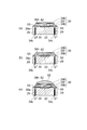
- FIG. 3A is a schematic perspective view of the light emitting unit of the first embodiment
- FIG. 3B is a schematic cross-sectional view taken along the line AA
- FIG. 3C is a first modification of the light emitting unit
- FIG. 3D is a schematic cross-sectional view of a second modification of the light emitting section
- FIG. 3E is a schematic perspective view of a third modification of the light emitting section.
- FIG. 4A is a schematic perspective view of the solid-state lighting device according to the second embodiment, and FIG.
- FIG. 4B is a schematic cross-sectional view of the vicinity of the light emitting unit along the line BB.
- 5A is a schematic cross-sectional view of a first modification of the optical unit of the second embodiment
- FIG. 5B is a schematic cross-sectional view of the second modification
- FIG. 5C is a third modification.
- It is a schematic diagram.
- 6A is a schematic cross-sectional view of an optical unit having a hologram element
- FIG. 6B is a schematic cross-sectional view of a modified example thereof
- FIG. 6C is a schematic cross-sectional view of a structure further including a lens.
- FIG. 7A is a schematic cross-sectional view illustrating a method for forming a phosphor layer
- FIG. 7A is a schematic cross-sectional view illustrating a method for forming a phosphor layer
- FIG. 7B is a schematic cross-sectional view of an application example to a back-side incident structure
- FIG. It is a schematic cross section of an application example.
- FIG. 8A is a schematic perspective view of a solid state lighting device according to the third embodiment
- FIG. 8B is a schematic perspective view of a front cover portion
- FIG. 8C is a solid state lighting device excluding the front cover portion. It is a model perspective view. It is a schematic cross section of the solid-state lighting device concerning 3rd Embodiment.
- FIG. 10A is a schematic perspective view of a first modification of the first light guide
- FIG. 10B is a schematic perspective view of a second modification.
- 11A is a schematic perspective view of a modified example of the front cover, FIG.
- FIG. 11B is a schematic perspective view of a second modified example of the first light guide
- FIG. 11C is a schematic perspective view of the heat conducting portion.
- Figure. It is a schematic cross section of the structure which provided the ferrule between the 2nd light guide and the opening part of a heat conductive part.
- FIG. 13A is a ray tracing diagram of the solid-state lighting device according to the third embodiment
- FIG. 13B is a schematic cross-sectional view taken along the line BB.
- It is a model perspective view which shows the beam spread of the laser beam from a semiconductor laser element.
- FIG. 15A is a schematic cross-sectional view of a first modification of the third embodiment
- FIG. 15B is a schematic diagram illustrating the optical axis.
- FIG. 15A is a schematic cross-sectional view of a first modification of the third embodiment
- FIG. 15B is a schematic diagram illustrating the optical axis.
- FIG. 15A is a schematic cross-sectional view of
- FIG. 16A is a schematic perspective view of a second modification of the third embodiment
- FIG. 16B is a schematic perspective view of the front cover portion
- FIG. 16C is a linear illumination excluding the front cover portion.
- FIG. 17A is a schematic cross-sectional view of the solid state lighting device according to the fourth embodiment
- FIG. 17B is a schematic cross-sectional view along the line BB
- FIG. 18A is a schematic cross-sectional view of the solid state lighting device according to the fifth embodiment
- FIG. 18B is a schematic cross-sectional view along the line BB.
- FIG. 19A is a schematic perspective view of a solid state lighting device according to the sixth embodiment, FIG.
- FIG. 19B is a schematic cross-sectional view taken along the line CC
- FIG. 19C is a ray tracing diagram
- 20A is a schematic perspective view of a horizontal one-dimensional collective solid-state lighting device
- FIG. 20B is a schematic perspective view of a vertical one-dimensional collective solid-state lighting device
- FIG. 20C is a two-dimensional collective solid-state lighting device. It is a model perspective view.
- It is a schematic diagram which shows the structure of the projector which is an example of the application example of a solid-state lighting apparatus. It is a block diagram which shows the function of a projector.
- FIG. 1 is a schematic perspective view illustrating the configuration of the solid-state lighting device according to the first embodiment.
- the solid state lighting device includes a light source unit 10, a light guide unit 20, and a light emitting unit 30.
- the light source unit (light engine) 10 includes a semiconductor laser 11 and a drive circuit 12.
- the semiconductor laser 11 is made of a nitride-based semiconductor material, and emits laser light in a blue-violet to blue wavelength range. If the solid state light emitting device is a semiconductor laser, it can be efficiently coupled to an optical fiber or the like with high brightness.
- the light emitting point on the end face of the semiconductor laser chip has a size of 10 ⁇ m or less, and its radiation angle (beam divergence) is as narrow as about 25 ° ⁇ 40 °.
- the drive circuit 12 supplies a predetermined voltage or current to the semiconductor laser 11. It is also possible to have a control circuit that provides a predetermined light output. Further, it can have a function of detecting the return light and stopping the driving of the semiconductor laser 11 when, for example, an abnormality is detected.
- the light source unit 10 can have an optical fiber 14 for transmitting the laser light from the semiconductor laser 11 and an optical coupling unit 13 such as a lens for condensing the laser light on the end of the optical fiber 14. Furthermore, an optical sensor that detects the return light RL1 for detecting an abnormality of the emitted light can be provided.
- Laser light includes multiple beams.
- the plurality of beams may branch the output of one semiconductor laser, or may be independent beams. When a plurality of beams emitted from a plurality of semiconductor lasers 11 are used, a higher output can be obtained.
- the light guide 20 can have a plurality of waveguides. Each waveguide transmits each of the plurality of laser beams G ⁇ b> 1 to the light emitting unit 30.
- the light guide 20 can have a plurality of waveguides. Each waveguide transmits each of the plurality of laser beams G ⁇ b> 1 to the light emitting unit 30.
- the light emitting unit 30 includes a heat conducting unit 34, a wavelength conversion layer 32, and an optical unit 39.
- the wavelength conversion layer 32 is provided at the center of the first surface 34 a of the heat conducting unit 34.
- the optical unit 39 is provided on the first surface 34a and the wavelength conversion layer 32, and has an upper surface, a side surface, and a lower surface.
- One end of each of the plurality of waveguides is disposed outside the central portion as viewed from above.
- Each of the plurality of laser beams G1 incident on the optical unit 39 from one end of each is guided and then irradiates the wavelength conversion layer 32.
- the wavelength conversion light having a wavelength longer than the wavelength of the laser light is emitted from the wavelength conversion layer 32 that has absorbed a plurality of laser lights.
- Mixed light of a plurality of laser beams and wavelength-converted light is emitted from the upper surface of the optical unit 39.
- the waveguide includes an optical fiber and the light guide unit 20 is a multi-core optical fiber, but the present invention is not limited to this.
- the laser light is incident from the back surface side, but the laser light may be incident from the side surface side of the optical unit 39.
- the light guide unit 20 can further include a connector 26 on the light emitting unit 30 side, a connector 23 fitted to the connector 26, and a connector 22 fitted to the light source unit 10. If it does in this way, when the distance of the light emission part 30 and the light source part 10 changes, what is necessary is just to set it as the length of the optical fiber 24 according to this distance.
- the waveguide has one end made of the first fiber ferrule 29, a second fiber ferrule 28, and an optical fiber 24. The first fiber ferrule 29 and the second fiber ferrule 28 are optically coupled.
- the connector 26 has a plurality of openings 26a and a fitting portion 26b surrounded by the plurality of openings 26a. Second fiber ferrules 28 are respectively inserted into the openings 26a.
- the plurality of second fiber ferrules 28 are arranged concentrically at equal intervals in the peripheral region of the connector 26.
- the plurality of first fiber ferrules 29 are also arranged in a concentric circle at equal intervals. If each diameter of the first fiber ferrule 29 is larger than each diameter of the second fiber ferrule 28, the laser light is incident on the first fiber ferrule 29 with high efficiency.
- the position of the first fiber ferrule 29 can be controlled with a stopper or the like.
- a heat-resistant adhesive or laser welding can be used for the fixing.
- the light emitting unit 30 includes a wavelength conversion light layer (phosphor layer) 32, a heat conducting unit 34, an optical unit 39, and a first solder layer (not shown).
- the wavelength conversion layer 32 is provided at the center of the first surface 34 a of the heat conducting unit 34.
- openings 34 c into which the first fiber ferrule 29 is inserted are arranged at equal intervals around the wavelength conversion layer 32. For example, when the laser light is in the wavelength range of blue to blue-violet light, yellow light can be obtained as wavelength converted light if the wavelength conversion layer 32 is made of a yellow phosphor. As a result, the mixed light can be made near white light.
- the heat conducting part 34 is made of, for example, a metal having a high thermal conductivity. Further, the first surface 34a preferably has a reflectance as high as 80% or higher, preferably 90% or higher, at a blue light wavelength.
- FIG. 2 is a schematic perspective view illustrating the fitting between the first connector and the heat conducting unit.
- a fitting portion 34d is provided on the second surface 34b side of the heat conducting portion 34 made of a metal having high heat conductivity.
- the connector 26 has a convex fitting part 26b, and the heat conducting part 34 has a concave fitting part 34d. For this reason, it can be easily attached and detached between the connector 26 and the heat conducting portion 34c.
- the unevenness of the fitting portion may be provided in reverse, not the unevenness but, for example, a spring may be used.
- a wavelength conversion layer 32 made of a circular thin reflective material and YAG (Yttrium Aluminum Garnet) is formed at the center of the first surface 34a.
- YAG Yttrium Aluminum Garnet
- each of the first fiber ferrules 29 which are one end portions of the plurality of waveguides is disposed outside the high luminance white light emitting region, and the high luminance white light emitting layer is thermally conductive. It is characterized in that it is directly formed on the base material of the portion 34. That is, by arranging a large number of the first fiber ferrules 29 outside the wavelength conversion layer 32, it is possible to increase the amount of light emitted from one area.
- the heat generation of the phosphor cannot be ignored as the brightness increases.
- the wavelength conversion layer 32 cannot be efficiently irradiated with blue light.
- an optical unit 39 is provided.
- the optical unit 39 has a structure in which a slope of total reflection is formed on the side surface and further totally reflected on the upper surface to irradiate the wavelength conversion layer 32 with a plurality of blue laser beams. If the guided blue laser light is directly applied to the phosphor and transmitted, the converted white light returns to the light guiding direction, and the efficiency is lowered. That is, the wavelength-converted light and the blue scattered light have no directivity and are difficult to control so as not to return to the optical fiber. In consideration of realistic energy saving, at least the return light needs to be suppressed to 10% or less of the total white light.
- the light guide unit 20 since the diameter is small, only part of the white light once diffused returns.
- the high-intensity, high-intensity light source uses a plurality of optical fibers, the area obtained by multiplying the cross-sectional area of the optical fibers by the number becomes the incident area of the return light, and the proportion of the return light increases accordingly.
- the optical fiber opening is disposed on the outer periphery of the diffuse white light emission at the center, the distance can be increased. If the distance is increased, the amount of incident light can be significantly reduced for diffused light.
- blue laser light with high directivity is guided so as to irradiate the wavelength conversion layer 32 through a narrow waveguide, and once converted into white light, it is difficult to return to the waveguide. For this reason, in the first embodiment, white light extraction efficiency can be improved.
- FIG. 3A is a schematic perspective view of the light-emitting portion
- FIG. 3B is a schematic cross-sectional view along the line AA
- FIG. 3C is a schematic cross-sectional view of a first modification of the light-emitting portion
- FIG. 3D is a schematic cross-sectional view of a second modification of the light emitting unit
- FIG. 3E is a schematic perspective view of a third modification of the light emitting unit.
- the optical unit 39 has an upper surface 39d, side surfaces, and a lower surface 39e. Further, the side surface includes an outer first inclined surface 39b and an inner second inclined surface 39c.
- the first fiber ferrule 29 is inserted into an opening 34 c provided in the heat conducting unit 34.
- the first inclined surface 39 b reflects the laser light g 1 emitted from the first fiber ferrule 29 and guides it toward the wavelength conversion layer 32.
- the second inclined surface 39 guides the laser light reflected by the first inclined surface 39b and irradiates the wavelength conversion layer 32 efficiently.
- the blue laser light irradiates the wavelength conversion layer 32 intensively through the gap 39a formed by the second inclined surface 39c.
- the laser light incident on the light emitting unit 30 is reflected or diffused by the wavelength conversion layer 32 or converted into scattered light by repeated reflection in the optical unit 39.
- the main parts of the blue-violet to blue scattered light and the wavelength converted light g2 such as yellow light are extracted from the upper surface 39d (GT).
- the lower surface 39e of the optical part 39 and the first surface 34a of the heat conducting part 34 are bonded with solder or adhesive made of eutectic metal or the like in an inert gas atmosphere.
- the layer 55 or the like can be used for contact. If it does in this way, the inside of the space
- gap 39a is filled with an inert gas, and the wavelength conversion layer 32 can be airtightly sealed. This structure can prevent the wavelength conversion layer 32 from being deteriorated. That is, the light emitting unit 30 including the mechanical strength and having high reliability can be realized.
- the wavelength conversion layer 32 can be formed by, for example, dispersing phosphor particles in a resin. *
- the angle of the laser light incident from the lower surface 39 e side of the optical unit 39 can be changed abruptly first by the photonic crystal 80. Since the photonic crystal 80 is physically forbidden except for the waveguide, the optical path can be bent at an angle close to a right angle. For this reason, it is unnecessary to form the first slope 39b by polishing or the like.
- the optical part 39 is not provided with a gap, has a high refractive index and has a core part 39f having a taper part near the center part, and a clad part 39h sandwiching the core part 39f from above and below. And can have.
- a portion other than the core portion 39f may be a photonic crystal. The function of the tapered portion will be described in detail in the second embodiment.
- the optical part 39 or the heat conducting part 34 may be polygonal. Even if the light emitting area is circular, if the optical part 39 and the base material have more flat parts, the processing of the parts themselves is easier and the cost can be reduced. Also, assembly is easy when combined with other parts. In this respect, the manufacturing cost can be reduced.
- FIG. 4A is a schematic perspective view of the solid-state lighting device according to the second embodiment
- FIG. 4B is a schematic cross-sectional view of the vicinity of the light emitting unit along the line BB.
- the waveguide includes the optical fiber 24, and the light guide unit 20 includes a multi-core fiber bundle.
- the laser beam g3 is introduced from one end of the waveguide to the side surface 49d of the optical unit 49.
- the side incident structure is characterized in that the optical unit 49 can be easily designed and heat radiation from the wavelength conversion layer 32 is efficient. That is, in the backside incident structure of the first embodiment, since the direction in which the first fiber ferrule 29 extends and the direction in which the generated heat in the wavelength conversion layer 32 is discharged are the same, heat dissipation is reduced.
- the optical part 49 has a structure in which a core part 49a having a high refractive index is sandwiched from above and below by a clad part 49b made of glass having a low refractive index. Therefore, highly directional laser light propagates through the core portion 49a and is not affected by scratches or dirt on the adhesive layer 55 made of solder material or the upper surface 49e of the optical portion 49. In addition, because of the planar structure, mass production and cost reduction are easy.
- a tapered portion 49c is provided at the tip of the core portion 49a instead of the internal slope on the gap side.
- the laser light is totally reflected and guided at the upper and lower refractive index interfaces, and is directed downward by the tapered portion 49c on the upper surface of the wavelength conversion layer 32, so that the wavelength conversion layer 32 is efficiently irradiated.
- the distribution of irradiation can be controlled by the shape of the tapered portion 49c. Therefore, the brightness of the minute light emitting surface can be controlled. Since the difference in refractive index between the clad portion 49a and the core portion 49b may be relatively small, the light distribution of white light emission in the wavelength conversion layer 32 is hardly affected.
- FIG. 5A is a schematic cross-sectional view of a first modification of the optical unit having a side-incident structure
- FIG. 5B is a schematic cross-sectional view of the second modification
- FIG. 5C is a schematic view of the third modification.
- laser light may be incident on the inside of the optical unit 49 having the gap 49g.
- the side surface and the outer periphery of the optical unit 49 and the first surface 34a of the heat conducting unit 34 can be bonded by an adhesive layer 55 made of an adhesive or the like.
- the gap may not be provided, and the laser beam may be incident from the side surface of the core portion 49a having a higher refractive index than the cladding portion 49b.
- the exit ends of the square glass ferrule 24f in which the four optical fibers 24 are integrated are each obliquely polished. Laser light bent at the slope of the square glass ferrule 24 f is incident on the side surface of the optical unit 49. For this reason, the number of components is reduced and the structure becomes simple.
- FIG. 6A is a schematic cross-sectional view of an optical unit having a hologram element
- FIG. 6B is a schematic cross-sectional view of a modification thereof
- FIG. 6C is a schematic cross-sectional view of a structure further including a lens.
- the hologram element 82 having a minute pattern is provided on the lower surface of the core portion 39f of the optical portion 39, the irradiation to the wavelength conversion layer 32 can be controlled with high accuracy.
- a hologram element 82 may be provided inside the core portion 39f. That is, since the incident light is laser light, the minute pattern can be a diffraction grating designed based on wave optics. Further, as shown in FIG. 6C, if a lens 88 is provided on the optical unit 39, the light distribution characteristic can be controlled.
- the lens 88 can be, for example, a concave surface, a convex surface, or an aspherical surface. In addition, although this figure represents the back surface incident structure, a side surface incident structure may be sufficient.
- FIG. 7A is a schematic cross-sectional view illustrating an example of the structure of the wavelength conversion layer
- FIG. 7B is a schematic cross-sectional view of an application example to the back-side incident structure
- FIG. 7C is an application to the side-surface incident structure. It is a schematic cross section of an example.
- the wavelength conversion layer 32 made of a phosphor layer has been shown as being applied to the first surface 34a of the heat conducting portion 34.
- the wavelength conversion layer 32 is modified as follows. You can also For example, as shown in FIG. 7A, it can be provided on the first surface of the reflecting member 84 made of a white ceramic plate or a silver thin plate.
- the second surface of the reflecting member and the first surface 34 a of the heat conducting unit 34 can be bonded by the adhesive layer 56. If it does in this way, an assembly process will become easy. In addition, since the wavelength conversion characteristics can be evaluated in advance, chromaticity adjustment is facilitated, and the yield can be increased.
- the optical unit 39 is provided so as to surround the wavelength conversion layer 32.
- FIG. 7C shows a side incident structure. With such a structure, the manufacturing process is simplified and mass productivity can be improved.
- FIG. 8A is a schematic perspective view of a solid state lighting device according to the third embodiment
- FIG. 8B is a schematic perspective view of a front cover portion
- FIG. 8C is a solid state lighting device excluding the front cover portion. It is a model perspective view.
- the linear solid-state lighting device 5 includes a semiconductor laser 11 as a first light source, a first light guide 38, a second light guide 27, a heat conducting unit 50, a front cover 70, Have
- the semiconductor laser 11 can emit laser light 11a in the ultraviolet to visible light wavelength range. If the semiconductor is a nitride material, it emits laser light in the ultraviolet to green wavelength range. When the semiconductor is made of a material such as InGaAlP or AlGaAs, laser light in the green to red wavelength range is emitted.
- the first laser light 11 a is guided through the second light guide 27 and then enters the first light guide 38.
- the first laser light 11 a incident on the first light guide 38 is guided upward in the first light guide 38 and upward from the exit surface 38 c exposed at the opening provided in the front cover 70. Released (emitted light G). If a phosphor layer is provided between the first light guide 38 and the heat conducting unit 50, the scattered light of the first laser light 11a and the wavelength converted light from the phosphor layer 40 are generated.
- the emitted light G can be mixed light such as white light.
- the width W may be 5 to 20 mm
- the height T may be 5 to 20 mm
- the length L may be 20 to 100 mm, and the like.
- FIG. 9 is a schematic cross-sectional view of a solid-state lighting device according to the third embodiment.
- FIG. 9 is a schematic cross-sectional view along the line AA in FIG.
- the 2nd light guide 27 has the 1st end surface 27a and the 2nd end surface 27b provided in the opposite side to the 1st end surface 27a.
- the first laser beam 11a introduced from the first end face 27a is guided and emitted from the second end face 27b.
- the second light guide 27 can be, for example, a thin glass rod or an optical fiber.
- the first light guide 38 has a bottom surface 38a, an emission surface 38c provided on the opposite side of the bottom surface 38a, and a first inclined surface 38d that forms an acute angle ⁇ with the bottom surface 38a.
- the bottom surface 38 c of the first light guide 38 includes a first incident region 38 b connected to the second end surface 27 b of the second light guide 27.
- the first laser light 11a incident on the first light guide 38 is emitted as scattered light upward from the emission surface 38c while being guided (emitted light G).
- the 1st light guide 38 shall consist of transparent resin or glass, for example.
- the heat conduction part 50 is provided with a first opening 50b that reaches the first surface 50a.
- the first light guide 38 is disposed on the first surface 50a side, and the second light guide 27 is provided in the first opening 50b.
- the front cover 70 can be disposed on the outer peripheral region of the first surface 50a of the heat conducting unit 50, for example. Since the beam spread of the first laser beam 11a incident from the semiconductor laser 11 as the first light source is small, the cross-sectional area S2 of the second light guide 27 perpendicular to the light guide direction 24 is the light guide direction. 34 may be smaller than the cross-sectional area S ⁇ b> 1 of the first light guide 38 that is orthogonal to 34.
- the heat conducting unit 50 is a heat conducting material made of a metal, ceramic such as AlN, etc.
- the 1st surface 50a of the heat conductive part 50 contains a metal, a light reflectivity can be raised.
- the scattered light and wavelength-converted light of the first laser light 11a that has passed through the phosphor layer 40 are reflected upward, and the light extraction efficiency can be increased.
- a groove or a recess for accommodating the first light guide 38 may be provided on the first surface 50 a of the heat conducting unit 50.
- the angle ⁇ formed by the bottom surface 38a and the first inclined surface 38d is appropriately selected to thereby select the first light guide 27.
- the amount of total reflection on the inclined surface 38d can be increased.
- the first light guide 38 and the second light guide 27 may have an integral structure made of the same material.
- first laser beam 11a is totally reflected at the interface between the first light guide 38 and the outside, so that the phosphor layer 40 can be irradiated with the first laser beam 11a more uniformly. it can.
- the first laser beam 11a is reflected by the first inclined surface 38d, the bottom surface 38a, the emission surface 38c, the end surface 38e, the surface 50a of the heat conducting unit 50, and the like of the first light guide 38.
- the end surface 38e and the side surfaces 38f, 38h are desirably inclined surfaces that form an acute angle with respect to the bottom surface 38a so that the first laser beam 11a is reflected by the bottom surface 38a. In this way, the wavelength conversion efficiency can be increased by irradiating the phosphor layer 40 with a smaller number of reflections.
- the cross section of the first inclined surface 38d along the line AA may be curved. The propagation of the first laser beam 11a in the second light guide 27 will be described in detail later.
- FIG. 10A is a schematic perspective view of a first modification of the first light guide
- FIG. 10B is a schematic perspective view of a second modification.
- the cross-sectional shape of the first light guide 38 is not limited to a rectangle, and may be a circle, an ellipse, a trapezoid, or the like.
- the exit surface 38c has a collective lens shape with controllable light distribution characteristics.
- a part of the side surfaces 38f and 38h on both sides of the emission surface 38c may be inclined.
- FIG. 11A is a schematic perspective view of a modified example of the front cover
- FIG. 11B is a schematic perspective view of a second modified example of the first light guide
- FIG. 11C is a schematic perspective view of the heat conducting portion.
- the front cover 70 may be provided so as to cover the side surface of the first light guide 38 and the side surface of the heat conducting unit 50.
- the inner width W70 of the front cover 70 is equal to or slightly wider than the width W38 of the first light guide 38, and is equal to or slightly wider than the width W50 of the heat conducting unit 50.
- a fixing structure such as fitting or screwing is provided between the front cover 70 and the heat conducting unit 50.
- FIG. 12 is a schematic cross-sectional view of a structure in which a ferrule is provided between the second light guide and the opening of the heat conducting unit.
- the second light guide 27 When the second light guide 27 is connected to the bottom surface 38 a of the first light guide 38 by contact and welding, the second light guide 27 can be optically coupled to the first light guide 38. Alternatively, optical coupling is possible even if a lens or index matching oil is used between the second light guide 27 and the first light guide 38.
- the fiber ferrule 29 in which the second light guide 27 is inserted is inserted into the first opening 50b, and the fiber ferrule 29 and the heat conducting unit 50 are press-fitted. Alternatively, it may be fixed by adhesion or welding.
- the second light guide 27 and the bottom surface 38a of the first light guide 38 are “photocoupled” when the laser light emitted from the second light guide 27 is the first light guide. It means that the light enters the bottom surface 38a.
- FIG. 13A is an optical path in the illumination apparatus according to the third embodiment
- FIG. 13B is a schematic cross-sectional view taken along the line BB.
- FIG. 13A shows the optical path of the first laser beam 11a by the ray tracing method of the illumination apparatus according to the third embodiment shown in FIG.
- the first laser beam 11a incident on the first light guide 38 and reflected by the first inclined surface 38d directly irradiates the phosphor layer 40 or is emitted to the emission surface 38c adjacent to the first inclined surface 38d. After the total reflection, the phosphor layer 40 is irradiated.
- most of the emitted wavelength converted light propagates while spreading from the surface of the phosphor layer 40 and is emitted to the outside from the emission surface 38c.
- the first laser beam 11a and the first wavelength that does not reach the wavelength-converted light due to the irradiation to the phosphor layer 40 are obtained.
- the laser beam 11a can be reflected in the direction of the phosphor layer 40. As a result, more wavelength-converted light is finally generated and emitted from the exit surface 30c.
- the first laser light 11 a that propagates while spreading along the light guide direction 34 is reflected by the side surfaces 30 f and 30 h of the first light guide 30, and the phosphor layer 40. (Light g1).
- the wavelength-converted light generated by the light g1 is emitted from the emission surface 30c while spreading upward.
- the scattered light of the laser light 11a that has not been wavelength-converted is emitted from the upper emission surface 38c. In this manner, the emission light G in which the scattered light of the first laser light 11a and the wavelength-converted light are mixed is emitted from the emission surface 38c.
- FIG. 14 is a schematic perspective view showing the spread of laser light from a semiconductor laser.
- the size of the light emitting point of the first laser beam 11a is, for example, 1 ⁇ m or less in the thickness direction of the light emitting layer and about 10 ⁇ m in the horizontal direction of the light emitting layer, and is smaller than the LED.
- the full width at half maximum ⁇ v in the vertical direction with respect to the light emitting layer of the semiconductor laser is in the range of 30 to 40 degrees
- the full width at half maximum ⁇ h in the horizontal direction is 10 to 25 degrees, and has sharp directivity.
- the first laser light 11a propagating in the second light guide 27 along the light guide direction 24 is the second end face 27b on the opposite side of the first end face 27a, or the first light guide. From the welded portion of the body 38 and the second light guide 27, the light enters the first light guide 38 through the incident region 38b.
- the second end face 27b of the second light guide 27 or the first light guide 37 and the second light guide The optical axis 21 of the first laser light 11a emitted from the welded portion of the light guide 27 to the first light guide 38 is such that the optical axis 21 passing through the center O1 of the second light guide 27 is the first.
- reflection occurs at the first inclined surface 38d.
- the light incident on the first inclined surface 38 d at an angle larger than the critical angle is totally reflected and propagates in the first light guide 38.
- the cross-sectional shape of the second light guide 27 is not limited to a circle but may be an ellipse or a rectangle. Further, when the second light guide 27 is an optical fiber, the shape is flexible, so that the light source can be easily arranged.
- ⁇ Smoothness is generated on the exit surface of the lighting device in which a large number of LEDs are arranged.
- continuous and natural white light emission can be realized.
- FIG. 15A is a schematic cross-sectional view of a first modification of the third embodiment
- FIG. 15B is a schematic diagram illustrating the optical axis.
- the second light guide 27 may form an intersection angle ⁇ (where 0 ⁇ ⁇ 90 °) with respect to the bottom surface 38 a of the first light guide 38.
- intersection angle ⁇ is close to the inclination angle ⁇ of the first inclined surface 38d, total reflection is likely to occur, and light that escapes from the first inclined surface 38d to the outside can be reduced.
- the optical axis of the first laser beam 11a passes through the center O2 of the second end face 27b and is refracted according to Snell's law with respect to the light guide direction 24.
- the optical axis 21a is on the extension of the light guide direction 24.
- the optical axis 21b is refracted as shown in FIG.
- the optical axis 21c is refracted as shown in FIG.
- FIG. 16A is a schematic perspective view of a second modification of the third embodiment
- FIG. 16B is a schematic perspective view of the front cover portion
- FIG. 16C is a solid state lighting device excluding the front cover portion. It is a model perspective view.
- the first opening provided in the heat conducting unit 50 may not be a hole that vertically penetrates the heat conducting unit 50.
- the first opening is a groove 50 c provided on the side surface of the heat conducting unit 50. Providing the groove 50c makes it easy to connect the second end face 27b of the second light guide 27 and the incident region 38b of the first light guide 38 by welding or the like. Alternatively, it is easy to dispose on the upper surface 50a of the heat conducting part 50 after welding.
- FIG. 17A is a schematic cross-sectional view of the solid state lighting device according to the fourth embodiment
- FIG. 17B is a schematic cross-sectional view along the line BB.
- a light scattering layer 42 in which a light scattering material is mixed with a liquid transparent resin and cured can be used.
- the light propagated in the light guide direction DG enters the light scattering layer 42, and the light scattered by the light scattering layer 42 is emitted upward.
- a part of the light reflected by the first surface 50 a of the heat conducting unit 50 is further reflected by the reflective layer 60 and emitted to the outside or can enter the phosphor layer 40.
- the light g5 reflected by the side surface 38f of the first light guide 38 in the first laser light 11a enters the light scattering layer 42 as shown in FIG.
- the light diffused by the light scattering layer 42 is emitted upward.
- the light g6 reflected by the side surface 38f is reflected by the first surface 50a of the heat conducting unit 50 and emitted from the emission surface 38c (emitted light G).
- FIG. 18A is a schematic cross-sectional view of the solid state lighting device according to the fifth embodiment
- FIG. 18B is a schematic cross-sectional view along the line BB.
- the phosphor layer is not provided between the bottom surface 38a of the first light guide 38 and the heat conducting unit 50, and is provided on at least one of the bottom surface 38a, the emission surface 38c, the end surface 38e, and the side surfaces 38f and 38h.
- the light scattering layer By providing the light scattering layer, light obtained by converting the first laser light 11a into scattered light is emitted from the emission surface 38c.
- high brightness light in the green to red wavelength range corresponding to the incident first laser light 11a can be emitted with a simple structure.
- FIG. 19A is a schematic perspective view of a solid state lighting device according to the sixth embodiment
- FIG. 19B is a schematic cross-sectional view along the line CC
- FIG. 19C is a ray tracing diagram.
- the second laser light 11b emitted from the semiconductor laser 11 as the second light source is guided along the light guide direction DG, and the vertical direction of the bottom surface 38a of the first light guide 38 is used.
- first light guide 38 has a first inclined surface 38d and a second inclined surface 38k that are symmetrical.
- the heat conducting unit 50 has a first opening 50b and a second opening 50d at positions that are substantially symmetrical.
- the luminance distribution can be made flatter. If the first laser beam 11a and the second laser beam 11b have substantially the same characteristics, the luminance distribution along the emission surface 38c can be easily made symmetrical. In this case, the laser light from one light source may be divided into first and second laser lights.
- FIG. 20A is a schematic perspective view of a horizontal one-dimensional collective solid-state lighting device
- FIG. 20B is a schematic perspective view of a vertical one-dimensional collective solid-state lighting device
- FIG. 20C is a two-dimensional collective solid-state lighting device. It is a model perspective view.
- FIG. 20A shows a one-dimensional assembly solid-state lighting device in which two solid-state lighting devices 5 are arranged in the light guide direction.
- FIG. 20B shows a one-dimensional assembly solid-state lighting device in which four solid-state lighting devices 6 are arranged in a direction substantially orthogonal to the light guide direction.
- FIG. 13C shows a two-dimensional collective solid state lighting device in which the solid state lighting devices 6 are arranged so as to be 2 ⁇ 2.
- the plurality of solid state lighting devices 6 can emit light simultaneously or individually.
- an inclined surface having the same inclination as the inclination (angle ⁇ ) of the first inclined surface 38 d can be provided inside the front cover 70.
- a slight gap can be provided between the first opening 50 b and the second light guide 27.
- linear illumination device that is easy to control the light distribution characteristics, increase the brightness, reduce the thermal resistance, and reduce the size and weight.
- These linear illumination devices may have a length L shorter than that of a linear illumination device for a copying machine. Further, since the laser beam can be introduced from the bottom surface side, the array arrangement is easy.
- lighting devices such as LEDs, halogen light bulbs, high intensity light sources such as HID (High Intensity Discharge), and lighting devices such as projectors have large housings due to the heat generated by the light sources.
- the projector includes a cooling fan and the like, and optical components such as a liquid crystal and a lens, a circuit, and the like are integrally incorporated in the housing. It is also necessary to take measures against heat dissipation from these expensive parts.
- the exhaust heat from the cooling fan is uncomfortable and the fan noise is loud.
- the solid-state lighting devices of the first to sixth embodiments can emit a light beam exceeding 1000 lumens with a diameter on the order of millimeters, thereby realizing a high-intensity, high-intensity white light source.
- the heat generating region in the light emitting unit 30 is only the wavelength conversion layer 32 which is a phosphor layer, and a small and lightweight white light emitting region can be realized.
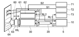
- FIG. 21 is a schematic diagram illustrating a configuration of a projector that is an example of an application example of the solid-state lighting device.
- the semiconductor laser generating a large amount of heat and the drive circuit are housed in the light source unit 10.
- the light emitting unit 30 connected to the light source unit 10 by the light guide unit 27 such as the optical fiber 24 can be small in size, light in weight, and low in heat generation, despite being capable of emitting a large amount of light and high luminance. If the light source unit 10 is installed, for example, under a desk or the like, the desk is widened, and exhaust heat and noise caused by a cooling fan can be suppressed.
- the projection unit 60 that projects an image on the screen 64 is provided with a shutter made of a liquid crystal device, a digital mirror device, or the like in front of the light emitting unit. Since the liquid crystal device has low power consumption, it generates little heat.
- the optical fiber 24 may be provided with a connector for optical signal transmission. Of course, an electrical signal transmission connector can also be provided. When the optical fiber bundle is passed through the free pipe so that the light emitting unit 30 can freely adjust the neck angle, the irradiation position can be adjusted with one touch.
- FIG. 22 is a block diagram illustrating functions of the projector.
- the projector includes a projection unit 60, the solid-state lighting device 5, a sweep signal drive unit 71, a return light sensor unit 73, and a video signal drive unit 72.
- the projection unit 60 includes an image unit 63, a sweep optical unit 61, and an external signal sensor unit 62.
- the video unit 63 may have a liquid crystal shutter or a digital mirror device.
- the laser beam G 1 emitted from the light source unit 10 propagates through the light guide unit 20 and enters the light emitting unit 30.
- the white light WL emitted from the light emitting unit 30 acts as a backlight for the video unit 63.
- the light source unit 10 can transmit the laser light G ⁇ b> 2 to the sweep optical unit 61.
- the return light RL1 from the optical unit 30 passes through the light guide unit 20 and enters the return light sensor unit 73.
- the return light RL1 includes laser light and wavelength converted light reflected by the light emitting unit 30.
- the return light sensor unit 73 may detect this decrease and stop driving the semiconductor laser in the light source unit 10. it can. That is, since the solid-state lighting device 5 has a self-diagnosis function for detecting that the emitted light is in the abnormal mode, it is possible to prevent the blue light and the like from being excessively emitted and to ensure safety.
- the video signal 63 is input to the video unit 63 from the video signal driving unit 72 and projected onto the screen 64.
- the sweep optical unit 61 receives the sweep signal S2 from the sweep signal driving unit 71.
- the signal transmission system is only light
- the solid state lighting devices according to the first to sixth embodiments are small in size, light in weight, low in heat generation, and easy to improve reliability.
- the illumination system that guides the laser beam to the light emitting part of the illumination with an optical fiber cable and unlike the illumination system using LEDs, filament light bulbs, HID lamps, etc., it is necessary to perform electrical wiring near the light emitting part of the illumination. Disappear.
- stage lighting can be used for projection and spot lighting. In this case, the color and brightness of the local part of the minute light emitting part can be adjusted, and although the resolution is low, a great effect can be obtained as an effect.
- both functions can be realized by using one small head. This can greatly change the concept of the stage and studio, and the effect is great.
- the external signal light sensor unit 62 detects an external light signal such as infrared rays
- the signal RL2 such as infrared rays and electricity is transmitted to the light source unit 10 and the semiconductor laser 11 can be controlled to be turned on or off.
- Such a solid state lighting device can be used as illumination for explosion-proof equipment, crime prevention lighting capable of image recording, and the like.
Landscapes
- Physics & Mathematics (AREA)
- General Physics & Mathematics (AREA)
- Optics & Photonics (AREA)
- Planar Illumination Modules (AREA)
- Semiconductor Lasers (AREA)
Abstract
Le dispositif d'éclairage à semi-conducteur de l'invention possède une partie source de lumière, une partie guidage de lumière et une partie luminescente. La partie source de lumière possède un laser à semi-conducteurs, et un circuit d'excitation commandant ce laser à semi-conducteurs, et émet une pluralité de lumières laser dans une plage de longueur d'onde allant du violet au bleu. La partie guidage de lumière possède une pluralité de guides d'onde guidant individuellement la pluralité de lumières laser. La partie luminescente possède : une partie conductrice de chaleur possédant une première face; une couche de conversion de longueur d'onde agencée sur la partie centrale de la première face; et une partie optique qui possède une face supérieure, une face latérale et une face inférieure, et dont au moins une partie de la face inférieure est en contact avec la première face. Une des parties extrémité de la pluralité de guides d'onde est individuellement disposée côté externe d'une partie centrale selon une vue d'en haut; et la pluralité de lumières laser provenant de cette partie extrémité et individuellement incidente sur la partie optique, irradie la couche de conversion de longueur d'onde après guidage. Une lumière convertie en longueur d'onde émise par la couche de conversion de longueur d'onde ayant absorbé la pluralité de lumières laser, et la lumière de diffusion produite par conversion de la pluralité de lumières laser à l'intérieur de la partie luminescente, sont émises à partir de la face supérieure de la partie optique.
Applications Claiming Priority (8)
| Application Number | Priority Date | Filing Date | Title |
|---|---|---|---|
| JP2011263763A JP2013118054A (ja) | 2011-12-01 | 2011-12-01 | 線状照明装置および集合線状照明装置 |
| JP2011-263763 | 2011-12-01 | ||
| JP2012-045833 | 2012-03-01 | ||
| JP2012045833 | 2012-03-01 | ||
| JP2012-092262 | 2012-04-13 | ||
| JP2012092262A JP2013222552A (ja) | 2012-04-13 | 2012-04-13 | 固体照明装置 |
| JP2012-253650 | 2012-11-19 | ||
| JP2012253650A JP2013211252A (ja) | 2012-03-01 | 2012-11-19 | 固体照明装置 |
Publications (1)
| Publication Number | Publication Date |
|---|---|
| WO2013081069A1 true WO2013081069A1 (fr) | 2013-06-06 |
Family
ID=48535517
Family Applications (1)
| Application Number | Title | Priority Date | Filing Date |
|---|---|---|---|
| PCT/JP2012/080980 Ceased WO2013081069A1 (fr) | 2011-12-01 | 2012-11-29 | Dispositif d'éclairage à semi-conducteur |
Country Status (1)
| Country | Link |
|---|---|
| WO (1) | WO2013081069A1 (fr) |
Cited By (4)
| Publication number | Priority date | Publication date | Assignee | Title |
|---|---|---|---|---|
| WO2014013923A1 (fr) * | 2012-07-17 | 2014-01-23 | 東芝ライテック株式会社 | Dispositif d'éclairage à semi-conducteurs |
| US10480762B2 (en) * | 2016-03-07 | 2019-11-19 | Panasonic Intellectual Property Management Co., Ltd. | Lighting fixture |
| US10705280B2 (en) | 2018-11-28 | 2020-07-07 | Sharp Kabushiki Kaisha | Light source module and light source device |
| JP2022116640A (ja) * | 2021-01-29 | 2022-08-10 | 京セラ株式会社 | 光接続構造及び照明システム |
Citations (4)
| Publication number | Priority date | Publication date | Assignee | Title |
|---|---|---|---|---|
| JP2007265626A (ja) * | 2006-03-27 | 2007-10-11 | Seiko Epson Corp | 照明装置及びプロジェクタ |
| JP2010035922A (ja) * | 2008-08-07 | 2010-02-18 | Olympus Corp | 光源装置およびこれを用いた内視鏡装置 |
| JP2011142000A (ja) * | 2010-01-07 | 2011-07-21 | Stanley Electric Co Ltd | 光源装置および照明装置 |
| JP2011243700A (ja) * | 2010-05-17 | 2011-12-01 | Sharp Corp | 発光装置、照明装置および車両用前照灯 |
-
2012
- 2012-11-29 WO PCT/JP2012/080980 patent/WO2013081069A1/fr not_active Ceased
Patent Citations (4)
| Publication number | Priority date | Publication date | Assignee | Title |
|---|---|---|---|---|
| JP2007265626A (ja) * | 2006-03-27 | 2007-10-11 | Seiko Epson Corp | 照明装置及びプロジェクタ |
| JP2010035922A (ja) * | 2008-08-07 | 2010-02-18 | Olympus Corp | 光源装置およびこれを用いた内視鏡装置 |
| JP2011142000A (ja) * | 2010-01-07 | 2011-07-21 | Stanley Electric Co Ltd | 光源装置および照明装置 |
| JP2011243700A (ja) * | 2010-05-17 | 2011-12-01 | Sharp Corp | 発光装置、照明装置および車両用前照灯 |
Cited By (4)
| Publication number | Priority date | Publication date | Assignee | Title |
|---|---|---|---|---|
| WO2014013923A1 (fr) * | 2012-07-17 | 2014-01-23 | 東芝ライテック株式会社 | Dispositif d'éclairage à semi-conducteurs |
| US10480762B2 (en) * | 2016-03-07 | 2019-11-19 | Panasonic Intellectual Property Management Co., Ltd. | Lighting fixture |
| US10705280B2 (en) | 2018-11-28 | 2020-07-07 | Sharp Kabushiki Kaisha | Light source module and light source device |
| JP2022116640A (ja) * | 2021-01-29 | 2022-08-10 | 京セラ株式会社 | 光接続構造及び照明システム |
Similar Documents
| Publication | Publication Date | Title |
|---|---|---|
| CN102901016B (zh) | 光源装置、照明装置、车辆用前照灯和车辆 | |
| US9863595B2 (en) | Light-emitting unit with optical plate reflecting excitation light and transmitting fluorescent light, and light-emitting device, illumination device, and vehicle headlight including the unit | |
| JP5323998B2 (ja) | 蛍光体、励起光源、光学システム、およびヒートシンクを備えた照明器具 | |
| US7736044B2 (en) | Indirect lighting device for light guide illumination | |
| JP5097548B2 (ja) | 照明システム | |
| JP6168611B2 (ja) | 光源、光合成装置、および光源付投影装置 | |
| JP6804448B2 (ja) | 発光デバイス | |
| JP2009510678A (ja) | 照明装置 | |
| JP5722068B2 (ja) | 光源装置、照明装置および車両用前照灯 | |
| WO2010001604A1 (fr) | Dispositif d’éclairage | |
| WO2013175706A1 (fr) | Élément optique, dispositif d'émission de lumière et dispositif de projection | |
| JP2013080638A (ja) | 集合線状照明装置およびその駆動方法、並びに灯具 | |
| JP2015088283A (ja) | 発光ユニットおよび照明装置 | |
| JP2019061796A (ja) | 照明器具 | |
| JP5538479B2 (ja) | Led光源及びそれを用いた発光体 | |
| WO2013081069A1 (fr) | Dispositif d'éclairage à semi-conducteur | |
| WO2014073237A1 (fr) | Dispositif d'éclairage à semi-conducteur | |
| WO2019128079A1 (fr) | Système de source lumineuse et dispositif d'éclairage | |
| JP6085204B2 (ja) | 発光装置 | |
| JP2013211252A (ja) | 固体照明装置 | |
| JP2013118054A (ja) | 線状照明装置および集合線状照明装置 | |
| JP2013222552A (ja) | 固体照明装置 | |
| JP2014203604A (ja) | 照明装置 | |
| CN210266742U (zh) | 一种ld激光光源模组 | |
| JP2014011034A (ja) | 固体照明装置 |
Legal Events
| Date | Code | Title | Description |
|---|---|---|---|
| 121 | Ep: the epo has been informed by wipo that ep was designated in this application |
Ref document number: 12854325 Country of ref document: EP Kind code of ref document: A1 |
|
| NENP | Non-entry into the national phase |
Ref country code: DE |
|
| 122 | Ep: pct application non-entry in european phase |
Ref document number: 12854325 Country of ref document: EP Kind code of ref document: A1 |