WO2013084366A1 - Dispositif de communication optique, appareil d'émission optique et procédé d'émission optique - Google Patents
Dispositif de communication optique, appareil d'émission optique et procédé d'émission optique Download PDFInfo
- Publication number
- WO2013084366A1 WO2013084366A1 PCT/JP2011/078835 JP2011078835W WO2013084366A1 WO 2013084366 A1 WO2013084366 A1 WO 2013084366A1 JP 2011078835 W JP2011078835 W JP 2011078835W WO 2013084366 A1 WO2013084366 A1 WO 2013084366A1
- Authority
- WO
- WIPO (PCT)
- Prior art keywords
- optical
- light
- phase
- unit
- transmission
- Prior art date
- Legal status (The legal status is an assumption and is not a legal conclusion. Google has not performed a legal analysis and makes no representation as to the accuracy of the status listed.)
- Ceased
Links
Images


Classifications
-
- H—ELECTRICITY
- H04—ELECTRIC COMMUNICATION TECHNIQUE
- H04B—TRANSMISSION
- H04B10/00—Transmission systems employing electromagnetic waves other than radio-waves, e.g. infrared, visible or ultraviolet light, or employing corpuscular radiation, e.g. quantum communication
- H04B10/50—Transmitters
- H04B10/501—Structural aspects
- H04B10/503—Laser transmitters
- H04B10/505—Laser transmitters using external modulation
- H04B10/5057—Laser transmitters using external modulation using a feedback signal generated by analysing the optical output
- H04B10/50577—Laser transmitters using external modulation using a feedback signal generated by analysing the optical output to control the phase of the modulating signal
Definitions
- the present invention relates to an optical communication device, an optical transmitter, and an optical transmission method, and more particularly to an optical communication device, an optical transmitter, and an optical transmission method using an optical phase modulation method.
- the digital coherent reception method is a reception method in which a phase modulation method (Phase Shift Keying), a coherent reception (Coherent Detection) technique, and a digital signal processing (Digital Signal processing) technique are combined.
- Digital coherent reception systems are required for long-distance optical fiber transmission such as optical signal-to-noise (Optical Signal to Noise Ratio) tolerance characteristics, chromatic dispersion tolerance characteristics, and polarization mode dispersion tolerance characteristics. Excellent characteristics.
- phase modulation method information is put on the phase of light on the transmission side, and the information is restored by detecting the phase of light on the reception side.
- phase modulation schemes binary phase modulation scheme (BPSK) and quaternary phase shift keying (QPSK) are attracting attention, especially from the balance of transmission characteristics, ease of implementation, and cost. Yes.
- a polarization multiplexed 4-phase modulation method that multiplexes and transmits a quaternary phase modulation signal with excellent frequency utilization efficiency with two orthogonal polarizations. It is actively researched and developed for practical application.
- the polarization multiplexing quaternary phase modulation method is also called DP-QPSK (Dual Polarization-Quadrature Phase Shift Keying).
- DP-QPSK Double Polarization-Quadrature Phase Shift Keying
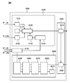
- FIG. 9 is a block diagram showing an example of the configuration of an optical transmitter used in quaternary optical phase modulation (QPSK).
- the optical transmitter 6100 includes a light source 6101, a phase modulation unit 6102, a drive unit I 6103, a drive unit Q 6104, a branching unit 6105, and a voltage control unit 6106.
- the phase modulation unit 6102 includes a CW optical branching unit 6107, a modulator I6108, a modulator Q6109, a shift unit 6110, and a mixing unit 6111.
- the light source 6101 outputs CW (Continuous Wave) light.
- the CW light branching unit 6107 branches the CW light output from the light source 6101 and outputs the branched light to the modulator I 6108 and the modulator Q 6109.
- the drive unit I6103 generates a voltage corresponding to the data I that is information to be transmitted, and applies the generated voltage to the modulator I6108.
- Drive unit Q6104 generates a voltage corresponding to data Q that is information to be transmitted, and applies the generated voltage to modulator Q6109.
- I and Q correspond to the I axis and Q axis of the constellation. That is, the data I determines the I-axis value of the symbol corresponding to the information to be transmitted. Similarly, data Q determines the Q-axis value of the symbol corresponding to the information to be transmitted.
- the modulator I6108 modulates one of the CW lights branched by the CW light branching unit 6107 based on the voltage generated by the driving unit I6103.
- a Mach-Zehnder type modulator (hereinafter referred to as a Mach-Zehnder type light) having a dielectric such as lithium niobate (LiNbO 3 ) as an optical waveguide is used.
- a modulator Since such a Mach-Zehnder type optical modulator is well known, detailed description thereof is omitted here.
- modulator Q6109 modulates the other of the CW light branched by CW light branching unit 6107 based on the voltage generated by driving unit Q6104.
- the phase modulation unit 6102 has a quaternary phase modulator in which the Mach-Zehnder type optical modulator described above is nested.
- shift section 6110 changes the phase of the light output from modulator Q6109.
- the shift unit 6110 changes the phase of the light output from the modulator Q6109 by ⁇ / 2 [radian].
- the shift unit 6110 outputs the shifted light to the mixing unit 6111.
- the mixing unit 6111 mixes the light output from the modulator I 6108 and the light output from the shift unit 6110. Next, the mixing unit 6111 outputs the mixed light to the branching unit 6105.
- the branching unit 6105 branches the light output from the phase modulation unit 6102.
- the branching unit 6105 outputs the branched light to the voltage control unit 6106.
- the voltage control unit 6106 controls the phase modulation unit 6102 based on the light branched by the branching unit 6105. Specifically, voltage control unit 6106 controls direct current (DC) voltage applied to modulator I 6108, modulator Q 6109, and shift unit 6110. Next, the operation of the voltage control unit 6106 will be described in detail with reference to the drawings.
- DC direct current
- FIG. 10A is a diagram for explaining the relationship between the electrical signal of information to be transmitted and the characteristics of the modulator.
- the characteristic of the modulator means a change in transmitted light intensity of the modulator with respect to the driving voltage.
- FIG. 10B schematically shows a phase-modulated optical signal.
- the modulator I6108 is applied with the sum of the DC voltage output from the voltage control unit 6106 and the voltage output from the drive unit I6103 as the drive voltage.
- the phase of light is modulated using a Mach-Zehnder type optical modulator
- the light output corresponding to “0” / “1”, which is information to be transmitted matches the adjacent peak point of transmitted light intensity.
- the voltage generated by the drive unit (hereinafter referred to as drive amplitude) is adjusted.
- the drive amplitude is adjusted so that the phase of the light transmitted through the Mach-Zehnder optical modulator becomes equal to a voltage that changes by ⁇ [radian].
- a voltage that is half the voltage at which the phase of the light transmitted through the Mach-Zehnder optical modulator changes by ⁇ [radian] is V ⁇ [V].
- the voltage control unit 6106 then adjusts the modulator I6108 and the modulator I6108 so that the average value of the drive amplitude corresponding to “0” / “1” that is information to be transmitted matches the minimum (Null) point of the transmitted light intensity of the modulator.
- the DC voltage applied to modulator Q6109 is adjusted.
- the voltage control unit 6106 sets the average value of the drive amplitude corresponding to the information to be transmitted to one of V ⁇ [V], 3V ⁇ [V],... Shown in FIG. Adjust the DC voltage.
- Patent Document 1 discloses an example of a configuration of a transmitter that adjusts a DC voltage applied to a modulator as described above.
- this transmitter adjusts the DC voltage applied to the modulator so that the average value of the drive amplitude corresponding to the information to be transmitted matches the minimum point of the light transmission intensity of the modulator.
- the modulator according to Patent Document 1 light from the second light source is input as backward light from the output side of the modulator, and the intensity of the backward light is measured on the input side of the modulator.
- the direct current voltage applied to the modulator is controlled so that the intensity of the backward light is minimized.
- the DC voltage is adjusted so that the average value of the drive amplitude corresponding to the information to be transmitted matches the minimum point of the light transmission intensity of the modulator. JP 2009-081747 A (paragraph “0026”)
- the modulator described in Patent Document 1 has a problem that the correspondence between the information to be transmitted and the phase of the light after the modulator modulates is not fixed.
- the reason why the correspondence relationship between the phase of the light after modulation by the modulator and the information to be transmitted is not fixed will be described in detail.
- the phase of the modulated light corresponding to “0” / “1” that is information to be transmitted is “ ⁇ ” / “0” [radian].
- the correspondence between the information to be transmitted and the phase of the modulated light in this case is referred to as “negative logic”.
- the correspondence relationship between the value of the DC voltage applied to the modulator and whether it is “positive logic” or “negative logic” varies depending on individual differences in the modulator, temperature changes, changes with time, and the like.
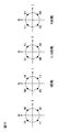
- phase modulation method for example, as shown in FIG. 11, four types of phase states can exist for one type of information to be transmitted.
- the horizontal axis in the figure is the in-phase axis (In-phase: I axis) in the QPSK system, and the vertical axis is the orthogonal axis (Quadrature-phase: Q axis).
- phase modulation corresponding to the I axis and the Q axis “positive logic” and “negative logic” can be taken, respectively, and there are the following four combinations. That is, when both the I axis and Q axis operate with positive logic (positive logic, positive logic), when only the I axis is inverted (negative logic, positive logic), when both the I axis and Q axis are inverted (negative logic, Negative logic) and when only the Q axis is inverted (positive logic, negative logic).
- four types of light of ⁇ / 4, 3 ⁇ / 4, 5 ⁇ / 4, and 7 ⁇ / 4 corresponding to the combinations described above as the phase state of light with respect to one type of information “00” to be transmitted.
- the object of the present invention is to determine the correspondence between the phase of the modulated light and the information to be transmitted in the optical transmitter using the related phase modulator, which is the problem described above.
- An object of the present invention is to provide an optical communication device, an optical transmitter, and an optical transmission method for solving the problem that the configuration of the optical receiver becomes complicated.
- An optical communication apparatus includes an optical transmitter that outputs transmission light that is phase-modulated based on transmission information, an optical receiver that receives and demodulates phase-modulated light, and an optical receiver that transmits part of the transmission light.
- An optical feedback unit, and a light transmitter that outputs continuous light, a phase modulation unit that phase-modulates the continuous light based on transmission information, and a control that controls the operation of the phase modulation unit The optical receiver acquires the reception information by demodulating the transmission light obtained from the optical feedback unit, and sends the reception information to the control unit.
- the control unit is based on the transmission information and the reception information. Controls the operation of the phase modulator.
- An optical transmitter of the present invention includes: a light source that outputs continuous light; a phase modulation unit that outputs transmission light obtained by phase-modulating continuous light based on transmission information; and a control unit that controls the operation of the phase modulation unit.
- the control unit acquires reception information obtained by demodulating the transmission light, and controls the operation of the phase modulation unit based on the transmission information and the reception information.
- the optical transmission method of the present invention phase-modulates continuous light based on transmission information, outputs phase-modulated transmission light, acquires reception information obtained by demodulating transmission light, and performs phase modulation based on transmission information and reception information. To control.
- the optical communication device the optical transmitter, and the optical transmission method of the present invention, it is possible to determine the correspondence between the phase of light after modulation in the optical transmitter and the information to be transmitted with a simple configuration.
- FIG. 1 is a block diagram showing a configuration of an optical communication apparatus according to the first embodiment of the present invention.
- FIG. 2A is a table showing a relationship (in the case of positive logic) between transmission information and the phase of modulated light in the optical transmitter according to the first embodiment of the present invention.
- FIG. 2B is a table showing a relationship (in the case of negative logic) between transmission information and the phase of modulated light in the optical transmitter according to the first embodiment of the present invention.
- FIG. 3 is a flowchart showing the operation of the optical communication apparatus according to the first embodiment of the present invention.
- FIG. 4 is a block diagram showing a configuration of an optical transmission system using the optical communication apparatus according to the first embodiment of the present invention.
- FIG. 5 is a table for explaining the operation of the optical communication apparatus according to the second embodiment of the present invention.
- FIG. 6 is a flowchart showing the operation of the optical communication apparatus according to the second embodiment of the present invention.
- FIG. 7 is a block diagram showing a configuration of an optical transmitter according to the third embodiment of the present invention.
- FIG. 8 is a block diagram showing a configuration of an optical communication apparatus according to the fourth embodiment of the present invention.
- FIG. 9 is a block diagram showing an example of the configuration of an optical transmitter used in quaternary optical phase modulation (QPSK).
- FIG. 10A is a diagram for explaining the relationship between the electrical signal of information to be transmitted and the characteristics of the modulator.
- FIG. 10B schematically shows a phase-modulated optical signal.
- FIG. 10A is a diagram for explaining the relationship between the electrical signal of information to be transmitted and the characteristics of the modulator.
- FIG. 10B schematically shows a phase-modulated optical signal.
- FIG. 10A is a
- FIG. 11 is a diagram showing the relationship between information to be transmitted and the phase of modulated light in the QPSK system.
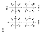
- FIG. 12A is a diagram showing the relationship between transmission information and the phase of light after modulation when rotating by “+ ⁇ / 2” in the QPSK system.
- FIG. 12B is a diagram illustrating a relationship between transmission information and the phase of light after modulation in the case of rotating “ ⁇ / 2” in the QPSK system.
- FIG. 1 is a block diagram showing a configuration of an optical communication apparatus 1000 according to the first embodiment of the present invention.
- the optical communication apparatus 1000 includes an optical transmitter 1100, an optical receiver 1200, and an optical feedback unit 1300.
- the optical transmitter 1100 outputs transmission light that is phase-modulated based on transmission information.
- the optical receiver 1200 receives and demodulates the phase-modulated light.
- the optical feedback unit 1300 introduces part of the transmission light output from the optical transmitter 1100 to the optical receiver 1200.
- the optical transmitter 1100 includes a light source 1110 that outputs continuous light, a phase modulation unit 1120 that modulates the phase of continuous light based on transmission information, and a control unit 1130 that controls the operation of the phase modulation unit 1120.
- the optical receiver 1200 acquires reception information by demodulating the transmission light obtained from the optical feedback unit 1300, and sends this reception information to the control unit 1130. Then, control section 1130 controls the operation of phase modulation section 1120 based on transmission information and reception information.
- the light source 1110 for example, a laser diode (LD) or the like can be used.
- the phase modulation unit 1120 performs phase modulation on continuous light output from the light source 1110 and outputs phase-modulated transmission light.
- phase modulation method for example, MPSK (M Phase Shift Keying, M is an integer), QAM (Quadrature Amplitude Modulation), or the like can be used.
- the phase modulation unit 1120 can be configured to include a Mach-Zehnder type optical modulator. Examples of the optical waveguide material include lithium niobate (LiNbO). 3 ) Or the like can be used.
- the optical receiver 1200 is not limited to the transmission light input from the optical feedback unit 1300, and can receive and demodulate the phase-modulated signal light from the communication partner. By adopting such a configuration, the optical communication apparatus 1000 according to the present embodiment can control the operation of the optical transmitter 1100 based on transmission information and reception information.
- the control unit 1130 includes a drive unit 1131 that adds a drive signal to the phase modulation unit 1120 and a determination unit 1132 that compares transmission information and reception information and controls the drive unit based on the comparison result. can do.
- the drive signal includes a modulation signal corresponding to transmission information and a DC signal for adjusting the average value of the modulation signal.
- the optical feedback unit 1300 also includes an optical branching unit 1310 that branches a part of the transmission light, and an optical switching unit 1320 that introduces either the branched transmission light or the signal light from the communication partner to the optical receiver 1200. It can be set as the structure provided with. For example, a fiber-type optical coupler or a planar lightwave circuit (PLC) can be used for the optical branching unit 1310. Further, the optical switching unit 1320 can be a mechanical optical switch using a micro mirror or a waveguide optical switch using a thermo-optic effect.
- the optical receiver 1200 restores information regarding the phase of the input light by demodulating the phase-modulated light. Then, information regarding the phase of the restored light is sent to the determination unit 1132 as reception information.
- the information relating to the light phase may be information associated with the restored light phase, and for example, binary logic may be employed.
- the optical receiver 1200 may be configured to send a binary logic “0” associated in advance to the determination unit 1132 when the phase of the recovered light is “ ⁇ ” [radian].
- a demodulation method for example, a coherent reception method can be used.
- the phase modulation method will be described.
- optical phase mapping Between the information to be transmitted (transmission information) and the phase of the light after being modulated by the phase modulator 1120, as described in the background art, there are two types of correspondences (hereinafter referred to as “optical phase mapping”). ) Exists.
- 2A and 2B show examples of optical phase mapping. 2A shows the case of positive logic, and FIG.
- 2B shows the case of negative logic.
- 2A and 2B show the transmission information
- the lower stage shows the phase of the modulated light
- the upper stage transmission information corresponds to the phase of the modulated light in the lower stage.
- the determination unit 1132 compares the transmission information and the reception information. If the transmission information and the reception information match, the determination unit 1132 controls the drive unit 1131 so as to maintain the value of the DC signal added to the phase modulation unit 1120.
- the drive unit 1131 is controlled to change the value of the DC signal.
- information predetermined as transmission information can be used.
- the driving unit 1131 includes a modulation signal corresponding to the predetermined information and a driving signal (for example, a driving voltage) including a DC signal for adjusting the average value of the modulation signal. Is applied to the phase modulation unit 1120.
- the phase modulation unit 1120 modulates the continuous light based on the driving signal at this time, and outputs the modulated light as transmission light.
- the optical feedback unit 1300 branches the transmission light and inputs the branched transmission light to the optical receiver 1200.
- the optical receiver 1200 extracts the phase of the input transmission light, and sends the demodulated reception information to the determination unit 1132.
- the determination unit 1132 compares the received information with predetermined information.
- predetermined information For example, a case where the information shown in the upper part of FIG. 2A is input to the control unit 1130 as the predetermined information is considered.
- the optical phase mapping predetermined in the optical communication apparatus 1000 has the correspondence shown in FIG. 2A.
- the transmission light extracted by the optical receiver 1200 has the phase shown in the lower part of FIG. 2B.
- the determination unit 1132 is based on information predetermined as transmission information (upper part of FIG.
- the predetermined information is not limited to the case where information different from the transmission information transmitted to the communication partner is used, and a part of the transmission information can also be used.
- a known information pattern such as a frame header part or a training signal part included in the transmission information can be used. Examples of such known information patterns include PRBS (Pseudo Random Bit Stream).
- the transmission information is associated with the phase of light modulated by the phase modulation unit 1120.
- the transmission information information based on a combination of binary logics may be used as the transmission information.
- the minimum unit of transmission information is “0” or “1”.
- the minimum unit of transmission information is any one of “00”, “01”, “10”, and “11”.
- the drive unit 1131 controls the value of the DC signal added to the phase modulation unit 1120 so that the transmission information and the reception information match based on the comparison result described above.
- the phase modulation unit 1120 includes a Mach-Zehnder type optical modulator, a direct current (DC) voltage is used as a direct current signal.
- DC direct current
- the determination unit 1132 controls the drive unit 1131 to maintain the value of the DC voltage. To do.
- the determination unit 1132 controls the drive unit 1131 to change the value of the DC voltage.
- the width for changing the value of the DC signal added to the phase modulation unit 1120 will be described. The width for changing the DC signal is determined based on the relationship between the drive signal of the phase modulation unit 1120 and the transmitted light intensity of the phase modulation unit 1120.
- the phase modulation unit 1120 includes a Mach-Zehnder optical modulator
- the width for changing the DC voltage as the DC signal is 2V ⁇ [V].
- the range to be changed can be set to 2V ⁇ + 2V ⁇ ⁇ N (N is an even number) [V] within a range in which the Mach-Zehnder optical modulator is driven.
- FIG. 12A it demonstrates still more concretely using FIG. 12A.
- the drive unit 1131 is applying, for example, 3 V ⁇ [V] as a DC voltage to the phase modulation unit 1120.
- the optical phase mapping becomes negative logic as shown in the figure. If the predetermined optical phase mapping is positive logic, the transmission information and the reception information do not match.
- the determination unit 1132 controls the drive unit 1131 so as to change the value of the DC voltage to, for example, V ⁇ [V].
- the optical phase mapping can be changed to a predetermined positive logic.
- the predetermined optical phase mapping is negative logic, the transmission information and the reception information match. Therefore, the determination unit 1132 controls the drive unit 1131 so as to maintain the DC voltage value (3V ⁇ [V]) at this time.
- the phase modulation unit 1120 performs phase modulation on continuous light (CW) output from the light source 1110 based on transmission information (step S110).
- the drive unit 1131 included in the control unit 1130 applies a modulation signal corresponding to transmission information and a DC signal for adjusting the average value of the modulation signal to the phase modulation unit 1120.
- the optical transmitter 1100 outputs the phase-modulated transmission light to the optical feedback unit 1300 (step S120).
- the optical feedback unit 1300 introduces part of the transmission light output from the optical transmitter 1100 to the optical receiver 1200, and the optical receiver 1200 demodulates the transmission light and acquires reception information (step S130).
- the optical communication apparatus 1000 controls the phase modulation performed by the phase modulation unit 1120 based on the transmission information and the reception information in the control unit 1130 included in the optical transmitter 1100 (step S140). Specifically, first, the determination unit 1132 included in the control unit 1130 determines whether transmission information and reception information match (step S142). Then, based on the determination result at this time, the determination unit 1132 controls the modulation signal corresponding to the transmission information and the DC signal for adjusting the average value of the modulation signal. For example, when the transmission information and the reception information match (step S142 / YES), the determination unit 1132 controls the drive unit 1131 to maintain the value of the DC signal (step S144).
- the determination unit 1132 controls the drive unit 1131 to change the value of the DC signal (step S146).
- FIG. 4 is a block diagram showing a configuration of an optical transmission system 5000 using the optical communication apparatus 1000.
- the optical transmission system 5000 includes an optical communication device 1000A, an optical communication device 1000B, and an optical communication device 1000C.
- the optical communication apparatus 1000A and the optical communication apparatus 1000C are connected by a transmission line 5100.
- the optical communication device 1000B and the optical communication device 1000C are connected by a transmission line 5200.
- the optical communication device 1000C may be an optical receiver included in the optical communication device 1000A or the optical communication device 1000B.
- the number of optical communication devices connected to the optical communication device 1000C can be three or more.
- the optical communication apparatus 1000A performs transmission / reception with the optical communication apparatus 1000C via the transmission path 5100.
- the optical communication device 1000B performs transmission / reception with the optical communication device 1000C via the transmission path 5200.
- the optical communication device 1000C selects either the optical communication device 1000A or the optical communication device 1000B as an object to be communicated, switches as needed, and communicates with either the optical communication device 1000A or the optical communication device 1000B.
- the optical receiver on the communication partner side is configured to determine whether the optical phase mapping is positive logic or negative logic, there are the following problems. That is, the optical receiver provided in the optical communication device 1000C communicates with a plurality of optical communication devices.
- the optical receiver included in the optical communication device 1000C must determine whether the optical phase mapping is positive logic or negative logic for each of the plurality of optical communication devices. Therefore, there is a problem that the optical receiver needs to make the above determination every time the partner optical communication apparatus with which communication is performed is switched, and time is required for that.
- the optical communication apparatus can determine the optical phase mapping by itself. Therefore, the optical receiver that communicates with the optical communication apparatus according to the present embodiment can perform demodulation processing on the received signal assuming that the optical phase mapping has a predetermined relationship. As a result, in the optical receiver, it is possible to reduce the time for switching the optical communication device as the communication partner.
- the optical communication apparatus 2000 according to the present embodiment is different from the optical communication apparatus 1000 according to the first embodiment in the configuration of the determination unit 2132 included in the control unit 2130 of the optical transmitter 2100. Since other configurations are the same as those of the optical communication apparatus 1000, description thereof is omitted.
- the determination unit 2132 included in the optical communication apparatus 2000 according to the present embodiment compares the transmission information and the reception information. If the transmission information and the reception information match, the determination unit 2132 controls the drive unit 1131 to maintain the modulation signal. On the other hand, when the transmission information and the reception information do not match, the drive unit 1131 is controlled to invert the modulation signal.
- FIG. 5 is a table for explaining the operation of the optical communication apparatus 2000 according to the second embodiment.
- a predetermined optical phase mapping in the optical communication apparatus 2000 is “positive logic”. That is, the phase of the modulated light corresponding to “0” / “1” that is transmission information is determined to be “0” / “ ⁇ ” [radian].
- the driving unit 1131 applies a low voltage LOW (for example, 0 [V]) to the phase modulation unit 1120 as a modulation signal for the transmission information “0” according to positive logic.
- a low voltage LOW for example, 0 [V]
- a high voltage HIGH for example, 2V
- ⁇ [V] is applied to the phase modulator 1120 (from the first row to the third row in FIG. 5, FIG. 12A).
- the optical transmitter 2100 outputs transmission light that is phase-modulated based on transmission information.
- the optical feedback unit 1300 included in the optical communication apparatus 2000 introduces part of the transmission light output from the optical transmitter 2100 to the optical receiver 1200.
- the optical receiver 1200 acquires the reception information by demodulating the transmission light obtained from the optical feedback unit 1300 according to a predetermined positive logic, and sends this reception information to the control unit 2130.
- the determination unit 2132 included in the control unit 2130 compares the transmission information and the reception information.
- the determination unit 2132 controls the driving unit 1131 to maintain the modulation signal.
- the phase modulation unit 1120 actually operates with “negative logic”. Therefore, the determination unit 2132 controls the drive unit 1131 to invert the modulation signal. That is, the driving unit 1131 receives a high voltage HIGH (for example, 2V) as a modulation signal for the transmission information “0”. ⁇ [V]) is applied to the phase modulator 1120. For the transmission information “1”, a low voltage LOW (for example, 0 [V]) is applied as a modulation signal to the phase modulation unit 1120 (5th line in FIG. 5).
- a high voltage HIGH for example, 2V
- ⁇ [V] is applied to the phase modulator 1120.
- a low voltage LOW for example, 0 [V]
- the phase modulation unit 1120 operates with “negative logic”, the phase of the modulated light corresponding to “0” / “1” as transmission information is “0” / “ ⁇ ” [radian]. ] (Line 6 in FIG. 5).
- the optical transmitter 2100 outputs transmission light that is phase-modulated by inverting the modulation signal.
- the optical receiver 1200 receives this transmission light and demodulates it according to a predetermined positive logic to obtain reception information.
- the reception signal at this time matches the transmission information because the reception information is “0” / “1” with respect to the phase “0” / “ ⁇ ” [radian] of the modulated light based on positive logic. Received information is obtained (line 7 in FIG. 5).
- FIG. 6 is a flowchart showing the operation of the optical communication apparatus 2000 of the present embodiment.
- the phase modulation unit 1120 performs phase modulation on continuous light (Continuous Wave: CW) output from the light source 1110 based on transmission information (step S110).
- the drive unit 1131 included in the control unit 2130 applies a modulation signal corresponding to transmission information and a DC signal for adjusting the average value of the modulation signal to the phase modulation unit 1120.
- the optical transmitter 2100 outputs the phase-modulated transmission light to the optical feedback unit 1300 (step S120).
- the optical feedback unit 1300 introduces a part of the transmission light output from the optical transmitter 2100 to the optical receiver 1200, and the optical receiver 1200 demodulates the transmission light and obtains reception information (step S130).
- the operation so far is the same as the operation of the optical communication apparatus 1000 according to the first embodiment.
- the optical communication device 2000 controls the phase modulation performed by the phase modulation unit 1120 based on the transmission information and the reception information in the control unit 2130 included in the optical transmitter 2100 (step S240). Specifically, first, the determination unit 2132 included in the control unit 2130 determines whether transmission information and reception information match (step S242).
- the determination unit 2132 controls the modulation signal corresponding to the transmission information and the DC signal for adjusting the average value of the modulation signal. For example, when the transmission information and the reception information match (step S242 / YES), the determination unit 2132 controls the drive unit 1131 to maintain the modulation signal (step S244). On the other hand, when the transmission information and the reception information do not match (step S242 / NO), the determination unit 2132 controls the drive unit 1131 to invert the modulation signal (step S246). As described above, according to the optical communication apparatus 2000 of the present embodiment, the operation of the optical transmitter 2100 can be controlled based on transmission information and reception information.
- FIG. 7 is a block diagram showing a configuration of an optical transmitter 3100 according to the third embodiment of the present invention.
- the optical transmitter 3100 includes a light source 3110 that outputs continuous light, a phase modulation unit 3120 that outputs transmission light obtained by phase-modulating continuous light based on transmission information, and a control unit 3130 that controls the operation of the phase modulation unit 3120. .
- control section 3130 acquires reception information obtained by demodulating the transmission light, and controls the operation of phase modulation section 3120 based on the transmission information and the reception information.
- the reception information can be acquired from the optical communication apparatus that is the communication partner of the optical transmitter 3100.
- the control unit 3130 includes a drive unit 3131 that adds a drive signal to the phase modulation unit 3120, and a determination unit 3132 that compares transmission information and reception information and controls the drive unit based on the comparison result. can do.
- the drive signal includes a modulation signal corresponding to transmission information and a DC signal for adjusting the average value of the modulation signal.
- control unit 3130 is the same as the operation of the control unit 1130 according to the first embodiment or the control unit 2130 according to the second embodiment, and a description thereof will be omitted.
- the operation of the phase modulation unit 3120 can be controlled based on the transmission information and the reception information. Therefore, with a simple configuration, it is possible to determine the correspondence between the phase of light after modulation in the optical transmitter 3100 and the information to be transmitted.
- FIG. 8 is a block diagram showing a configuration of an optical communication apparatus 4000 according to the fourth embodiment of the present invention.
- the optical communication device 4000 includes an optical transmitter 4100, an optical receiver 4200, and an optical feedback unit 4300.
- the optical transmitter 4100 outputs transmission light that has undergone four-level phase modulation based on transmission information.
- the optical receiver 4200 digitally coherently receives and demodulates quaternary phase modulated light.
- the optical feedback unit 4300 introduces part of the transmission light output from the optical transmitter 4100 to the optical receiver 4200.
- the optical transmitter 4100 includes a light source 4110 that outputs continuous light, a phase modulation unit 4120 that performs quaternary phase modulation on continuous light based on transmission information, and a control unit that controls operations of the phase modulation unit 4120.
- the control unit includes a drive unit I4131, a drive unit Q4132, and a power supply unit 4133 as drive units, and a power supply control unit 4134 and comparison unit 4135 as determination units.
- the drive unit I 4131 generates a drive voltage that is a modulation signal corresponding to the data I that is transmission information.
- the drive part Q4132 produces
- the operations of the drive unit I 4131 and the drive unit Q 4132 are the same as those of the drive unit 1131 included in the optical communication apparatus 1000 according to the first embodiment.
- the phase modulation unit 4120 performs phase modulation on continuous light based on transmission information input to the optical transmitter 4100.
- the phase modulation unit 4120 can be realized by the phase modulation unit 6102 described in FIG. 9, for example.
- the transmission information is referred to as data I and data Q.
- the data I corresponds to the I axis of the constellation
- the data Q corresponds to the Q axis of the constellation.
- the optical receiver 4200 includes a local oscillation light source (Local Oscillator) 4210 and a 90-degree hybrid circuit 4220.
- the 90-degree hybrid circuit 4220 receives local oscillation light output from the local oscillation light source 4210 and phase-modulated light, and outputs in-phase (In Phase) signal light and quadrature (Quadrature Phase) signal light.
- the optical receiver 4200 further includes a photoelectric conversion unit (Photodiode) 4230, an analog / digital converter (Analog to Digital Converter) 4240, and a signal processing unit 4250.
- the photoelectric conversion unit 4230 photoelectrically converts the in-phase signal light and the quadrature signal light, and outputs the in-phase electric signal and the quadrature electric signal.
- the analog / digital conversion unit 4240 performs analog / digital conversion on the in-phase electrical signal and the quadrature electrical signal, and outputs the in-phase digital signal and the quadrature digital signal.
- the signal processing unit 4250 demodulates the in-phase digital signal and the quadrature digital signal, and outputs received information to the comparison unit 4135.
- the signal processing unit 4250 is realized, for example, by digital signal processing (DSP).
- the optical feedback unit 4300 also includes an optical branching unit 4310 that branches a part of the transmission light, and an optical switching unit 4320 that introduces one of the branched transmission light and the signal light from the communication partner to the optical receiver 4200. It can be set as the structure provided with.
- the optical switching unit 4320 can be a mechanical optical switch using a micro mirror or a waveguide optical switch using a thermo-optic effect.
- the comparison unit 4135 compares the reception information acquired by the signal processing unit 4250 with the data I and data Q that are transmission information.
- the comparison unit 4135 sends the comparison result to the power supply control unit 4134.
- the optical transmitter 4100 performs quaternary phase modulation on continuous light based on the data I and data Q, and outputs phase-modulated transmission light.
- the optical branching unit 4310 branches the transmission light output from the phase modulation unit 4120 and outputs a part of the branched transmission light to the optical switching unit 4320.
- the optical switching unit 4320 switches the optical path so that a part of the transmission light is introduced into the optical receiver 4200.
- the 90-degree hybrid circuit 4220 causes a part of transmission light input from the optical switching unit 4320 to interfere with output light from the local oscillation light source 4210.
- the photoelectric conversion unit 4230 photoelectrically converts the interference light interfered by the 90-degree hybrid circuit 4220 and performs coherent detection.
- the analog / digital conversion unit 4240 converts the electrical signal converted by the photoelectric conversion unit 4230 into a digital signal.
- the signal processing unit 4250 restores the digital signal to reception information and outputs the reception information to the comparison unit 4135.
- the subsequent operation is the same as the operation of the optical communication apparatus 1000 according to the first embodiment, and a description thereof will be omitted.
- phase modulation unit In an optical transmitter of quaternary phase modulation (QPSK), data I corresponding to the in-phase axis (In-phase: I axis) and data Q corresponding to the quadrature axis (Quadrature-phase: Q axis) are used. And the phase of the transmission light after being modulated by the phase modulation unit is not fixed. Therefore, as described above, four types of phase states shown in FIG. 11 can exist for one type of transmission information.
- QPSK quadrature-phase
- the operation of the optical transmitter 4100 can be controlled based on the transmission information and the reception information by adopting the above-described configuration. Therefore, with a simple configuration, it is possible to determine the correspondence between the phase of light after modulation in the optical transmitter 4100 and the data I and data Q that are information to be transmitted. Further, by adopting such a configuration, for example, when the optical transmitter 4100 is powered on, the phase of the modulated light and the transmission information are not dependent on the initial convergence stability point of the DC voltage as the DC signal. Can be held in a specific relationship.
- the optical communication device 4000 of the present embodiment even when the speed of information to be transmitted is 40 Gbit / s or 100 Gbit / s, the above correspondence control is not affected. . That is, there is no dependency on the bit rate in the above-described correspondence control. Furthermore, inexpensive and low-speed components can be used for the configuration of the optical feedback unit 4300 that introduces part of the transmission light output from the optical transmitter 4100 into the optical receiver 4200.
- the other configurations of the optical communication device 4000 are the same as the configurations of a normal QPSK optical transmitter and a digital coherent receiver, so that an increase in price can be minimized.
- the quaternary phase modulation method QPSK
- the present invention is not limited to this, and a polarization multiplexing method that multiplexes two orthogonally polarized waves and a multi-value amplitude phase modulation method such as 16QAM and 64QAM are used. It may be used. Even when these modulation schemes are used, according to the present embodiment, it is possible to determine the correspondence between the data I and data Q as transmission information and the phase of the modulated light.
- phase modulation unit 6102 having a nested structure When the phase modulation unit 6102 having a nested structure is used in the Mach-Zehnder type optical modulator shown in FIG. 9 as an optical transmitter corresponding to the quaternary phase modulation method (QPSK), it corresponds to the I / Q axis.
- Modulator I 6108 and modulator Q 6109 each perform binary optical phase modulation.
- the shift unit 6110 shown in FIG. 9 rotates one phase of the optical phase signal corresponding to the I / Q axis by “ ⁇ / 2” [radian].
- the mixing unit 6111 mixes the outputs from the modulator I 6108 and the modulator Q 6109 to generate quaternary phase modulated light.
- FIGS. 12A and 12B show the processing of the shift unit 6110 do not increase the uncertainty in optical phase mapping.
- FIG. 12A shows the relationship between the transmission information and the phase of the modulated light when the rotation by the shift unit 6110 is “+ ⁇ / 2” [radian] rotation.
- FIG. 12B shows the relationship between the transmission information and the phase of the modulated light when the rotation by the shift unit 6110 is “ ⁇ / 2” [radian].
- Optical communication device 1100, 2100, 3100, 4100, 6100
- Light source 1120, 3120, 4120, 6102 Phase modulation unit 1130, 2130, 3130 Control Unit 1131, 3131 drive unit 1132, 2132, 3132 determination unit 1200, 4200 optical receiver 1300, 4300 optical feedback unit 1310, 4310 optical branch unit 1320, 4320 optical switching unit 4131, 6103 drive unit I 4132, 6104 Drive part Q 4133 Power supply unit 4134 Power supply control unit 4135 Comparison unit 4210 Local oscillation light source 4220 90 degree hybrid circuit 4230 Photoelectric conversion unit 4240 Analog / digital conversion unit 4250 Signal processing unit 5000 Optical transmission system 5100, 5200 Transmission path 6105 Branching unit 6106 Voltage control unit 6107 CW optical branching unit 6108 modulator I 6109 modulator Q 6110 Shift unit 6111 Mixing unit
Landscapes
- Physics & Mathematics (AREA)
- Optics & Photonics (AREA)
- Electromagnetism (AREA)
- Engineering & Computer Science (AREA)
- Computer Networks & Wireless Communication (AREA)
- Signal Processing (AREA)
- Optical Communication System (AREA)
Abstract
La présente invention vise à résoudre le problème dans lequel, dans un appareil d'émission optique utilisant un appareil de décalage de phase, il devient difficile d'établir une correspondance entre la phase d'une lumière décalée et des informations qui sont émises, compliquant ainsi la configuration d'un appareil de réception optique de celui-ci. Ce dispositif de communication optique comprend : un appareil d'émission optique qui délivre en sortie une lumière d'émission qui est décalée en phase sur la base d'informations d'émission ; un appareil de réception optique qui reçoit et démodule la lumière décalée en phase ; et une unité de rétroaction optique qui introduit une partie de la lumière d'émission à l'appareil de réception optique. L'appareil d'émission optique comprend en outre une source lumineuse qui délivre en sortie une lumière séquentielle, une unité de décalage de phase qui décale en phase la lumière séquentielle sur la base des informations d'émission, et une unité de commande qui commande le fonctionnement de l'unité de décalage de phase. L'appareil de réception optique acquiert des informations de réception par démodulation de la lumière émise qui est obtenue provenant de l'unité de rétroaction optique et émet les informations de réception à l'unité de commande. L'unité de commande commande le fonctionnement de l'unité de décalage de phase sur la base des informations d'émission et des informations de réception.
Priority Applications (2)
| Application Number | Priority Date | Filing Date | Title |
|---|---|---|---|
| JP2013548048A JP5907175B2 (ja) | 2011-12-07 | 2011-12-07 | 光通信装置、光送信器および光送信方法 |
| PCT/JP2011/078835 WO2013084366A1 (fr) | 2011-12-07 | 2011-12-07 | Dispositif de communication optique, appareil d'émission optique et procédé d'émission optique |
Applications Claiming Priority (1)
| Application Number | Priority Date | Filing Date | Title |
|---|---|---|---|
| PCT/JP2011/078835 WO2013084366A1 (fr) | 2011-12-07 | 2011-12-07 | Dispositif de communication optique, appareil d'émission optique et procédé d'émission optique |
Publications (1)
| Publication Number | Publication Date |
|---|---|
| WO2013084366A1 true WO2013084366A1 (fr) | 2013-06-13 |
Family
ID=48573763
Family Applications (1)
| Application Number | Title | Priority Date | Filing Date |
|---|---|---|---|
| PCT/JP2011/078835 Ceased WO2013084366A1 (fr) | 2011-12-07 | 2011-12-07 | Dispositif de communication optique, appareil d'émission optique et procédé d'émission optique |
Country Status (2)
| Country | Link |
|---|---|
| JP (1) | JP5907175B2 (fr) |
| WO (1) | WO2013084366A1 (fr) |
Cited By (2)
| Publication number | Priority date | Publication date | Assignee | Title |
|---|---|---|---|---|
| JP2016045340A (ja) * | 2014-08-22 | 2016-04-04 | 富士通オプティカルコンポーネンツ株式会社 | 光通信装置及び光変調器の制御方法 |
| JP2016045341A (ja) * | 2014-08-22 | 2016-04-04 | 富士通オプティカルコンポーネンツ株式会社 | 光通信装置及び光変調器の制御方法 |
Citations (4)
| Publication number | Priority date | Publication date | Assignee | Title |
|---|---|---|---|---|
| JPH11266200A (ja) * | 1998-03-18 | 1999-09-28 | Fujitsu Ltd | 光ファイバ通信のための方法並びに該方法の実施に使用される装置及びシステム |
| JP2010178090A (ja) * | 2009-01-29 | 2010-08-12 | Fujitsu Ltd | 光通信システムおよび光受信器 |
| JP2011069924A (ja) * | 2009-09-24 | 2011-04-07 | Nippon Telegr & Teleph Corp <Ntt> | Qpsk変調器 |
| JP2011527842A (ja) * | 2008-07-08 | 2011-11-04 | 日本電気株式会社 | xPSKトランスミッタの位相変調のタイミングを設定する方法及びシステム |
-
2011
- 2011-12-07 WO PCT/JP2011/078835 patent/WO2013084366A1/fr not_active Ceased
- 2011-12-07 JP JP2013548048A patent/JP5907175B2/ja active Active
Patent Citations (4)
| Publication number | Priority date | Publication date | Assignee | Title |
|---|---|---|---|---|
| JPH11266200A (ja) * | 1998-03-18 | 1999-09-28 | Fujitsu Ltd | 光ファイバ通信のための方法並びに該方法の実施に使用される装置及びシステム |
| JP2011527842A (ja) * | 2008-07-08 | 2011-11-04 | 日本電気株式会社 | xPSKトランスミッタの位相変調のタイミングを設定する方法及びシステム |
| JP2010178090A (ja) * | 2009-01-29 | 2010-08-12 | Fujitsu Ltd | 光通信システムおよび光受信器 |
| JP2011069924A (ja) * | 2009-09-24 | 2011-04-07 | Nippon Telegr & Teleph Corp <Ntt> | Qpsk変調器 |
Cited By (2)
| Publication number | Priority date | Publication date | Assignee | Title |
|---|---|---|---|---|
| JP2016045340A (ja) * | 2014-08-22 | 2016-04-04 | 富士通オプティカルコンポーネンツ株式会社 | 光通信装置及び光変調器の制御方法 |
| JP2016045341A (ja) * | 2014-08-22 | 2016-04-04 | 富士通オプティカルコンポーネンツ株式会社 | 光通信装置及び光変調器の制御方法 |
Also Published As
| Publication number | Publication date |
|---|---|
| JP5907175B2 (ja) | 2016-04-26 |
| JPWO2013084366A1 (ja) | 2015-04-27 |
Similar Documents
| Publication | Publication Date | Title |
|---|---|---|
| Sakamoto et al. | 50-Gb/s 16 QAM by a quad-parallel Mach-Zehnder modulator | |
| US8676060B2 (en) | Quadrature amplitude modulation signal generating device | |
| US8072669B2 (en) | Methods and apparatus for generating 16-QAM-modulated optical signal | |
| JP6263915B2 (ja) | 帯域内管理データ変調 | |
| US8934782B2 (en) | Transmission method, reception method, transmitter apparatus, and receiver device | |
| US9853739B2 (en) | Optical transmitter and method for controlling bias of optical modulator | |
| US8873953B2 (en) | Multiple-symbol polarization switching for differential-detection modulation formats | |
| US8077375B2 (en) | Method and apparatus for generating 8-QAM-modulated optical signal | |
| JP5009963B2 (ja) | Qpsk変調器 | |
| CN101626274A (zh) | 星型十六进制光信号的生成方法、光发射机和系统 | |
| US20230336248A1 (en) | Reconfigurable optical transceiver for use with multiple modulation techniques | |
| JP5907175B2 (ja) | 光通信装置、光送信器および光送信方法 | |
| Sakamoto et al. | Coherent synthesis of optical multilevel signals by electrooptic digital-to-analog conversion using multiparallel modulator | |
| JP4809270B2 (ja) | 光送信装置及び方法 | |
| Sakamoto et al. | 50-km SMF transmission of 50-Gb/s 16 QAM generated by quad-parallel MZM | |
| JP5131601B2 (ja) | 光変調信号発生装置 | |
| Yu et al. | Single-carrier advanced modulation formats | |
| JP2009027441A (ja) | 光送信回路 | |
| JP4531010B2 (ja) | 光位相変復調回路および光位相変復調方法 | |
| JP5215934B2 (ja) | 光変調装置、光変調装置の制御方法および光送信器 | |
| Seimetz | High spectral efficiency phase and quadrature amplitude modulation for optical fiber transmission—Configurations, trends, and reach | |
| Agarwal et al. | Principle of Coherence Optical Systems-Current Applications and Future Challenges | |
| Sakamoto et al. | High-bit-rate optical QAM | |
| Ha et al. | Multi-Dimensional Optical Transmission based on QAM-PIRFSK-DPSK Optical Modulation | |
| Sakamoto et al. | Electro-optic synthesis of multi-level coherent signals |
Legal Events
| Date | Code | Title | Description |
|---|---|---|---|
| 121 | Ep: the epo has been informed by wipo that ep was designated in this application |
Ref document number: 11876893 Country of ref document: EP Kind code of ref document: A1 |
|
| ENP | Entry into the national phase |
Ref document number: 2013548048 Country of ref document: JP Kind code of ref document: A |
|
| NENP | Non-entry into the national phase |
Ref country code: DE |
|
| 122 | Ep: pct application non-entry in european phase |
Ref document number: 11876893 Country of ref document: EP Kind code of ref document: A1 |