WO2013102992A1 - Matériau pour élément organique électroluminescent et élément utilisant ce matériau - Google Patents
Matériau pour élément organique électroluminescent et élément utilisant ce matériau Download PDFInfo
- Publication number
- WO2013102992A1 WO2013102992A1 PCT/JP2012/008429 JP2012008429W WO2013102992A1 WO 2013102992 A1 WO2013102992 A1 WO 2013102992A1 JP 2012008429 W JP2012008429 W JP 2012008429W WO 2013102992 A1 WO2013102992 A1 WO 2013102992A1
- Authority
- WO
- WIPO (PCT)
- Prior art keywords
- group
- unsubstituted
- substituted
- carbon atoms
- ring
- Prior art date
- Legal status (The legal status is an assumption and is not a legal conclusion. Google has not performed a legal analysis and makes no representation as to the accuracy of the status listed.)
- Ceased
Links
- UNPMAYVIGYIFHY-UHFFFAOYSA-N c(cc1)ccc1-[n](c1ccccc1c1c2)c1ccc2-c(cc1)cc(c2c3cccc2)c1[n]3-c(cc1)cc2c1[o]c(cc1)c2cc1-[n]1c2ccccc2c2c1cccc2 Chemical compound c(cc1)ccc1-[n](c1ccccc1c1c2)c1ccc2-c(cc1)cc(c2c3cccc2)c1[n]3-c(cc1)cc2c1[o]c(cc1)c2cc1-[n]1c2ccccc2c2c1cccc2 UNPMAYVIGYIFHY-UHFFFAOYSA-N 0.000 description 1
Images

Classifications
-
- C—CHEMISTRY; METALLURGY
- C07—ORGANIC CHEMISTRY
- C07D—HETEROCYCLIC COMPOUNDS
- C07D405/00—Heterocyclic compounds containing both one or more hetero rings having oxygen atoms as the only ring hetero atoms, and one or more rings having nitrogen as the only ring hetero atom
- C07D405/14—Heterocyclic compounds containing both one or more hetero rings having oxygen atoms as the only ring hetero atoms, and one or more rings having nitrogen as the only ring hetero atom containing three or more hetero rings
-
- C—CHEMISTRY; METALLURGY
- C07—ORGANIC CHEMISTRY
- C07B—GENERAL METHODS OF ORGANIC CHEMISTRY; APPARATUS THEREFOR
- C07B59/00—Introduction of isotopes of elements into organic compounds ; Labelled organic compounds per se
- C07B59/002—Heterocyclic compounds
-
- C—CHEMISTRY; METALLURGY
- C07—ORGANIC CHEMISTRY
- C07D—HETEROCYCLIC COMPOUNDS
- C07D409/00—Heterocyclic compounds containing two or more hetero rings, at least one ring having sulfur atoms as the only ring hetero atoms
- C07D409/14—Heterocyclic compounds containing two or more hetero rings, at least one ring having sulfur atoms as the only ring hetero atoms containing three or more hetero rings
-
- C—CHEMISTRY; METALLURGY
- C07—ORGANIC CHEMISTRY
- C07D—HETEROCYCLIC COMPOUNDS
- C07D471/00—Heterocyclic compounds containing nitrogen atoms as the only ring hetero atoms in the condensed system, at least one ring being a six-membered ring with one nitrogen atom, not provided for by groups C07D451/00 - C07D463/00
- C07D471/02—Heterocyclic compounds containing nitrogen atoms as the only ring hetero atoms in the condensed system, at least one ring being a six-membered ring with one nitrogen atom, not provided for by groups C07D451/00 - C07D463/00 in which the condensed system contains two hetero rings
- C07D471/04—Ortho-condensed systems
-
- C—CHEMISTRY; METALLURGY
- C07—ORGANIC CHEMISTRY
- C07D—HETEROCYCLIC COMPOUNDS
- C07D471/00—Heterocyclic compounds containing nitrogen atoms as the only ring hetero atoms in the condensed system, at least one ring being a six-membered ring with one nitrogen atom, not provided for by groups C07D451/00 - C07D463/00
- C07D471/12—Heterocyclic compounds containing nitrogen atoms as the only ring hetero atoms in the condensed system, at least one ring being a six-membered ring with one nitrogen atom, not provided for by groups C07D451/00 - C07D463/00 in which the condensed system contains three hetero rings
- C07D471/14—Ortho-condensed systems
-
- C—CHEMISTRY; METALLURGY
- C07—ORGANIC CHEMISTRY
- C07D—HETEROCYCLIC COMPOUNDS
- C07D491/00—Heterocyclic compounds containing in the condensed ring system both one or more rings having oxygen atoms as the only ring hetero atoms and one or more rings having nitrogen atoms as the only ring hetero atoms, not provided for by groups C07D451/00 - C07D459/00, C07D463/00, C07D477/00 or C07D489/00
- C07D491/02—Heterocyclic compounds containing in the condensed ring system both one or more rings having oxygen atoms as the only ring hetero atoms and one or more rings having nitrogen atoms as the only ring hetero atoms, not provided for by groups C07D451/00 - C07D459/00, C07D463/00, C07D477/00 or C07D489/00 in which the condensed system contains two hetero rings
- C07D491/04—Ortho-condensed systems
- C07D491/044—Ortho-condensed systems with only one oxygen atom as ring hetero atom in the oxygen-containing ring
- C07D491/048—Ortho-condensed systems with only one oxygen atom as ring hetero atom in the oxygen-containing ring the oxygen-containing ring being five-membered
-
- C—CHEMISTRY; METALLURGY
- C07—ORGANIC CHEMISTRY
- C07D—HETEROCYCLIC COMPOUNDS
- C07D491/00—Heterocyclic compounds containing in the condensed ring system both one or more rings having oxygen atoms as the only ring hetero atoms and one or more rings having nitrogen atoms as the only ring hetero atoms, not provided for by groups C07D451/00 - C07D459/00, C07D463/00, C07D477/00 or C07D489/00
- C07D491/12—Heterocyclic compounds containing in the condensed ring system both one or more rings having oxygen atoms as the only ring hetero atoms and one or more rings having nitrogen atoms as the only ring hetero atoms, not provided for by groups C07D451/00 - C07D459/00, C07D463/00, C07D477/00 or C07D489/00 in which the condensed system contains three hetero rings
- C07D491/14—Ortho-condensed systems
- C07D491/147—Ortho-condensed systems the condensed system containing one ring with oxygen as ring hetero atom and two rings with nitrogen as ring hetero atom
-
- C—CHEMISTRY; METALLURGY
- C07—ORGANIC CHEMISTRY
- C07D—HETEROCYCLIC COMPOUNDS
- C07D495/00—Heterocyclic compounds containing in the condensed system at least one hetero ring having sulfur atoms as the only ring hetero atoms
- C07D495/02—Heterocyclic compounds containing in the condensed system at least one hetero ring having sulfur atoms as the only ring hetero atoms in which the condensed system contains two hetero rings
- C07D495/04—Ortho-condensed systems
-
- C—CHEMISTRY; METALLURGY
- C07—ORGANIC CHEMISTRY
- C07D—HETEROCYCLIC COMPOUNDS
- C07D519/00—Heterocyclic compounds containing more than one system of two or more relevant hetero rings condensed among themselves or condensed with a common carbocyclic ring system not provided for in groups C07D453/00 or C07D455/00
-
- C—CHEMISTRY; METALLURGY
- C09—DYES; PAINTS; POLISHES; NATURAL RESINS; ADHESIVES; COMPOSITIONS NOT OTHERWISE PROVIDED FOR; APPLICATIONS OF MATERIALS NOT OTHERWISE PROVIDED FOR
- C09B—ORGANIC DYES OR CLOSELY-RELATED COMPOUNDS FOR PRODUCING DYES, e.g. PIGMENTS; MORDANTS; LAKES
- C09B57/00—Other synthetic dyes of known constitution
-
- C—CHEMISTRY; METALLURGY
- C09—DYES; PAINTS; POLISHES; NATURAL RESINS; ADHESIVES; COMPOSITIONS NOT OTHERWISE PROVIDED FOR; APPLICATIONS OF MATERIALS NOT OTHERWISE PROVIDED FOR
- C09K—MATERIALS FOR MISCELLANEOUS APPLICATIONS, NOT PROVIDED FOR ELSEWHERE
- C09K11/00—Luminescent materials, e.g. electroluminescent or chemiluminescent
- C09K11/06—Luminescent materials, e.g. electroluminescent or chemiluminescent containing organic luminescent materials
-
- H—ELECTRICITY
- H05—ELECTRIC TECHNIQUES NOT OTHERWISE PROVIDED FOR
- H05B—ELECTRIC HEATING; ELECTRIC LIGHT SOURCES NOT OTHERWISE PROVIDED FOR; CIRCUIT ARRANGEMENTS FOR ELECTRIC LIGHT SOURCES, IN GENERAL
- H05B33/00—Electroluminescent light sources
- H05B33/12—Light sources with substantially two-dimensional [2D] radiating surfaces
- H05B33/14—Light sources with substantially two-dimensional [2D] radiating surfaces characterised by the chemical or physical composition or the arrangement of the electroluminescent material, or by the simultaneous addition of the electroluminescent material in or onto the light source
-
- H—ELECTRICITY
- H10—SEMICONDUCTOR DEVICES; ELECTRIC SOLID-STATE DEVICES NOT OTHERWISE PROVIDED FOR
- H10K—ORGANIC ELECTRIC SOLID-STATE DEVICES
- H10K85/00—Organic materials used in the body or electrodes of devices covered by this subclass
- H10K85/60—Organic compounds having low molecular weight
- H10K85/649—Aromatic compounds comprising a hetero atom
- H10K85/657—Polycyclic condensed heteroaromatic hydrocarbons
-
- C—CHEMISTRY; METALLURGY
- C09—DYES; PAINTS; POLISHES; NATURAL RESINS; ADHESIVES; COMPOSITIONS NOT OTHERWISE PROVIDED FOR; APPLICATIONS OF MATERIALS NOT OTHERWISE PROVIDED FOR
- C09K—MATERIALS FOR MISCELLANEOUS APPLICATIONS, NOT PROVIDED FOR ELSEWHERE
- C09K2211/00—Chemical nature of organic luminescent or tenebrescent compounds
- C09K2211/10—Non-macromolecular compounds
- C09K2211/1003—Carbocyclic compounds
- C09K2211/1011—Condensed systems
-
- C—CHEMISTRY; METALLURGY
- C09—DYES; PAINTS; POLISHES; NATURAL RESINS; ADHESIVES; COMPOSITIONS NOT OTHERWISE PROVIDED FOR; APPLICATIONS OF MATERIALS NOT OTHERWISE PROVIDED FOR
- C09K—MATERIALS FOR MISCELLANEOUS APPLICATIONS, NOT PROVIDED FOR ELSEWHERE
- C09K2211/00—Chemical nature of organic luminescent or tenebrescent compounds
- C09K2211/10—Non-macromolecular compounds
- C09K2211/1018—Heterocyclic compounds
- C09K2211/1025—Heterocyclic compounds characterised by ligands
- C09K2211/1029—Heterocyclic compounds characterised by ligands containing one nitrogen atom as the heteroatom
-
- C—CHEMISTRY; METALLURGY
- C09—DYES; PAINTS; POLISHES; NATURAL RESINS; ADHESIVES; COMPOSITIONS NOT OTHERWISE PROVIDED FOR; APPLICATIONS OF MATERIALS NOT OTHERWISE PROVIDED FOR
- C09K—MATERIALS FOR MISCELLANEOUS APPLICATIONS, NOT PROVIDED FOR ELSEWHERE
- C09K2211/00—Chemical nature of organic luminescent or tenebrescent compounds
- C09K2211/10—Non-macromolecular compounds
- C09K2211/1018—Heterocyclic compounds
- C09K2211/1025—Heterocyclic compounds characterised by ligands
- C09K2211/1029—Heterocyclic compounds characterised by ligands containing one nitrogen atom as the heteroatom
- C09K2211/1033—Heterocyclic compounds characterised by ligands containing one nitrogen atom as the heteroatom with oxygen
-
- C—CHEMISTRY; METALLURGY
- C09—DYES; PAINTS; POLISHES; NATURAL RESINS; ADHESIVES; COMPOSITIONS NOT OTHERWISE PROVIDED FOR; APPLICATIONS OF MATERIALS NOT OTHERWISE PROVIDED FOR
- C09K—MATERIALS FOR MISCELLANEOUS APPLICATIONS, NOT PROVIDED FOR ELSEWHERE
- C09K2211/00—Chemical nature of organic luminescent or tenebrescent compounds
- C09K2211/10—Non-macromolecular compounds
- C09K2211/1018—Heterocyclic compounds
- C09K2211/1025—Heterocyclic compounds characterised by ligands
- C09K2211/1029—Heterocyclic compounds characterised by ligands containing one nitrogen atom as the heteroatom
- C09K2211/1037—Heterocyclic compounds characterised by ligands containing one nitrogen atom as the heteroatom with sulfur
-
- C—CHEMISTRY; METALLURGY
- C09—DYES; PAINTS; POLISHES; NATURAL RESINS; ADHESIVES; COMPOSITIONS NOT OTHERWISE PROVIDED FOR; APPLICATIONS OF MATERIALS NOT OTHERWISE PROVIDED FOR
- C09K—MATERIALS FOR MISCELLANEOUS APPLICATIONS, NOT PROVIDED FOR ELSEWHERE
- C09K2211/00—Chemical nature of organic luminescent or tenebrescent compounds
- C09K2211/10—Non-macromolecular compounds
- C09K2211/1018—Heterocyclic compounds
- C09K2211/1025—Heterocyclic compounds characterised by ligands
- C09K2211/1044—Heterocyclic compounds characterised by ligands containing two nitrogen atoms as heteroatoms
-
- C—CHEMISTRY; METALLURGY
- C09—DYES; PAINTS; POLISHES; NATURAL RESINS; ADHESIVES; COMPOSITIONS NOT OTHERWISE PROVIDED FOR; APPLICATIONS OF MATERIALS NOT OTHERWISE PROVIDED FOR
- C09K—MATERIALS FOR MISCELLANEOUS APPLICATIONS, NOT PROVIDED FOR ELSEWHERE
- C09K2211/00—Chemical nature of organic luminescent or tenebrescent compounds
- C09K2211/10—Non-macromolecular compounds
- C09K2211/1018—Heterocyclic compounds
- C09K2211/1025—Heterocyclic compounds characterised by ligands
- C09K2211/1044—Heterocyclic compounds characterised by ligands containing two nitrogen atoms as heteroatoms
- C09K2211/1048—Heterocyclic compounds characterised by ligands containing two nitrogen atoms as heteroatoms with oxygen
-
- C—CHEMISTRY; METALLURGY
- C09—DYES; PAINTS; POLISHES; NATURAL RESINS; ADHESIVES; COMPOSITIONS NOT OTHERWISE PROVIDED FOR; APPLICATIONS OF MATERIALS NOT OTHERWISE PROVIDED FOR
- C09K—MATERIALS FOR MISCELLANEOUS APPLICATIONS, NOT PROVIDED FOR ELSEWHERE
- C09K2211/00—Chemical nature of organic luminescent or tenebrescent compounds
- C09K2211/10—Non-macromolecular compounds
- C09K2211/1018—Heterocyclic compounds
- C09K2211/1025—Heterocyclic compounds characterised by ligands
- C09K2211/1088—Heterocyclic compounds characterised by ligands containing oxygen as the only heteroatom
-
- C—CHEMISTRY; METALLURGY
- C09—DYES; PAINTS; POLISHES; NATURAL RESINS; ADHESIVES; COMPOSITIONS NOT OTHERWISE PROVIDED FOR; APPLICATIONS OF MATERIALS NOT OTHERWISE PROVIDED FOR
- C09K—MATERIALS FOR MISCELLANEOUS APPLICATIONS, NOT PROVIDED FOR ELSEWHERE
- C09K2211/00—Chemical nature of organic luminescent or tenebrescent compounds
- C09K2211/10—Non-macromolecular compounds
- C09K2211/1018—Heterocyclic compounds
- C09K2211/1025—Heterocyclic compounds characterised by ligands
- C09K2211/1092—Heterocyclic compounds characterised by ligands containing sulfur as the only heteroatom
-
- H—ELECTRICITY
- H10—SEMICONDUCTOR DEVICES; ELECTRIC SOLID-STATE DEVICES NOT OTHERWISE PROVIDED FOR
- H10K—ORGANIC ELECTRIC SOLID-STATE DEVICES
- H10K50/00—Organic light-emitting devices
- H10K50/10—OLEDs or polymer light-emitting diodes [PLED]
- H10K50/11—OLEDs or polymer light-emitting diodes [PLED] characterised by the electroluminescent [EL] layers
Definitions
- the present invention relates to a novel compound suitable for a material for an organic electroluminescence device and an organic electroluminescence device using the same.
- Organic electroluminescence (EL) elements include a fluorescent type and a phosphorescent type, and an optimum element design has been studied according to each light emission mechanism. With respect to phosphorescent organic EL elements, it is known from their light emission characteristics that high-performance elements cannot be obtained by simple diversion of fluorescent element technology. The reason is generally considered as follows. First, since phosphorescence emission is emission using triplet excitons, the energy gap of the compound used for the light emitting layer must be large. This is because the value of the energy gap (hereinafter also referred to as singlet energy) of a compound usually refers to the triplet energy of the compound (in the present invention, the energy difference between the lowest excited triplet state and the ground state). This is because it is larger than the value of).
- a host material having a triplet energy larger than the triplet energy of the phosphorescent dopant material must first be used for the light emitting layer. I must. Furthermore, it is desirable to provide an electron transport layer and a hole transport layer adjacent to the light emitting layer, and use a compound having a triplet energy higher than that of the phosphorescent dopant material for the electron transport layer and the hole transport layer.
- a compound having a larger energy gap than the compound used for the fluorescent organic EL element is used for the phosphorescent organic EL element. The drive voltage of the entire element increases.
- hydrocarbon compounds having high oxidation resistance and reduction resistance which are useful in fluorescent elements, generally have a small energy gap because of the large spread of ⁇ electron clouds. Therefore, in a phosphorescent organic EL element, it is difficult to select such a hydrocarbon compound, and an organic compound containing a heteroatom such as oxygen or nitrogen is selected. As a result, the phosphorescent organic EL element is There is a problem that the lifetime is shorter than that of a fluorescent organic EL element.
- the exciton relaxation rate of the triplet exciton of the phosphorescent dopant material is much longer than that of the singlet exciton also greatly affects the device performance. That is, since light emitted from singlet excitons has a high relaxation rate that leads to light emission, it is difficult for excitons to diffuse into the peripheral layer of the light emitting layer (for example, a hole transport layer or an electron transport layer). Light emission is expected. On the other hand, light emission from triplet excitons is spin-forbidden and has a slow relaxation rate, so that excitons are likely to diffuse into the peripheral layer, and thermal energy deactivation occurs from other than specific phosphorescent compounds. End up. That is, control of the recombination region of electrons and holes is more important than the fluorescent organic EL element.
- Patent Document 1 discloses that as an organic EL device material, 3,3-biscarbazole in which two carbazoles are bonded to each other at the 3-position is used as a mother skeleton, and the two carbazoles have a dibenzothiophene ring. Disclosed are compounds having attached groups.
- Patent Document 2 discloses a compound having 3,3-biscarbazole as a mother skeleton and a heteroaromatic ring substituent bonded to the carbazole.
- Patent Document 3 discloses a compound in which a 3,3-biscarbazole unit is bonded to each of positions 2 and 8 of one dibenzofuran ring.
- An object of the present invention is to provide a material having a high triplet energy that can be used as a material of an organic EL element that emits phosphorescence.
- a compound represented by the following formula (1) L represents a single bond or a substituted or unsubstituted divalent monocyclic group.
- A represents a substituted or unsubstituted aryl group having 6 to 18 ring carbon atoms, a substituted or unsubstituted heteroaryl group having 13 to 18 ring atoms, or a substituted or unsubstituted alkyl group having 1 to 20 carbon atoms.
- X 1 to X 8 each represent CR 5 , CH or N
- Y represents an oxygen (O) atom or a sulfur (S) atom.
- Y is a sulfur (S) atom
- at least one of X 1 to X 8 is a nitrogen (N) atom.
- Any one of X 1 to X 4 is carbon (C) bonded to the carbazolylene group
- any one of X 5 to X 8 is a carbon (C) atom bonded to B.
- B is a substituted or unsubstituted arylcarbazolyl group having 19 to 30 ring atoms, a substituted or unsubstituted heteroarylcarbazolyl group having 19 to 30 ring atoms, or a substituent having 1 to 20 carbon atoms.
- R 1 to R 5 each independently represents a substituted or unsubstituted aryl group having 6 to 18 ring carbon atoms, a substituted or unsubstituted heteroaryl group having 5 to 18 ring atoms, a substituted or unsubstituted carbon;
- a and d each independently represents an integer of 0 to 4, and b and c each independently represents an integer of 0 to 3.
- R 1 may be the same or different.
- R 2 may be the same or different.
- R 3 may be the same or different.
- each R 4 may be the same or different.
- 2. The compound according to 1, wherein a to d in the formula (1) are 0. 3.
- 3. The compound according to 1 or 2, wherein L in the formula (1) is a single bond. 4). 3.
- An organic electroluminescence device comprising one or more organic thin film layers including a light emitting layer between a cathode and an anode, wherein at least one of the organic thin film layers comprises the compound according to any one of 1 to 5. 7).
- the organic thin film layer includes one or more light emitting layers, 6.
- the phosphorescent material contains a metal complex compound;
- the organic electroluminescence device according to 7 or 8, wherein the metal complex compound has a metal atom and a ligand selected from Ir, Pt, Os, Au, Cu, Re, and Ru. 10.
- the organic electroluminescence device according to any one of 6 to 10, wherein the maximum value of the emission wavelength is 430 nm or more and 720 nm or less. 12 12.
- the organic electroluminescence device according to any one of 7 to 11, which has an electron transport band between the light emitting layer and the cathode, and the electron transport band contains the compound according to any one of 1 to 5.
- the organic electroluminescence device which has a hole transport zone between the light emitting layer and the anode, and the hole transport zone contains the compound according to any one of 1 to 5. .
- a compound having a high triplet energy can be provided.
- This compound is suitable as a material for an organic EL device.
- the compound of the present invention is represented by the following formula (1).
- the compound of the formula (1) is effective for maintaining high luminous efficiency and lowering the driving voltage in blue to green phosphorescent devices and white phosphorescent devices that require particularly high triplet energy.
- a material that confines high triplet energy is required.
- the compound of the present invention has two carbazole skeletons, and a condensed heteroaromatic ring having a high triplet energy is bonded to the nitrogen atom of the carbazole, and the triplet energy is maintained in the condensed heteroaromatic ring.
- the compound of the present invention can reduce the hole injection barrier into the light emitting layer by selecting a specific condensed heteroaromatic ring.
- the compound of the present invention is a group of materials that can satisfy these two properties at the same time, and can greatly contribute to maintaining efficiency and reducing voltage in a phosphorescent device that requires high triplet energy.
- L represents a single bond or a substituted or unsubstituted divalent monocyclic group.
- the divalent monocyclic group include divalent residues such as a saturated ring, an unsaturated ring, an aromatic ring, and a heterocyclic ring.
- a benzene ring, a pyridine ring, a pyrimidine ring, a triazine ring, and a pyrazine examples thereof include divalent residues such as a ring and a cyclohexane ring.
- A represents a substituted or unsubstituted aryl group having 6 to 18 ring carbon atoms, a substituted or unsubstituted heteroaryl group having 13 to 18 ring atoms, or a substituted or unsubstituted alkyl group having 1 to 20 carbon atoms. Represents.
- X 1 to X 8 each represent CR 5 , CH or N, and Y represents an oxygen (O) atom or a sulfur (S) atom. However, when Y is a sulfur (S) atom, at least one of X 1 to X 8 is a nitrogen (N) atom. Any one of X 1 to X 4 is carbon (C) bonded to the carbazolylene group, and any one of X 5 to X 8 is a carbon atom bonded to B.
- B is a substituted or unsubstituted arylcarbazolyl group having 19 to 30 ring atoms, a substituted or unsubstituted heteroarylcarbazolyl group having 19 to 30 ring atoms, or a substituent having 1 to 20 carbon atoms.
- R 1 to R 5 each independently represents a substituted or unsubstituted aryl group having 6 to 18 ring carbon atoms, a substituted or unsubstituted heteroaryl group having 5 to 18 ring atoms, a substituted or unsubstituted carbon;
- a and d each independently represents an integer of 0 to 4, and b and c each independently represents an integer of 0 to 3.
- R 1 may be the same or different.
- R 2 may be the same or different.
- R 3 may be the same or different.
- each R 4 may be the same or different.
- the compounds represented by the formula (1) compounds in which a to d are 0 are preferable. As a result, since an extra electron conjugation between the substituent and the aromatic ring does not occur, good triplet energy can be obtained. Moreover, the compound whose L is a single bond among the compounds represented by Formula (1) is preferable. Thereby, since molecular weight is restrained small, the material with favorable thermal stability at the time of continuous vapor deposition is obtained. Examples of the compound of the formula (1) include compounds represented by any of the following formulas (2) to (17).
- L, A and B are the same as L, A and B in the formula (1), respectively.
- compounds wherein L is a single bond are preferred. Thereby, since molecular weight is restrained small, a material with favorable thermal stability at the time of continuous vapor deposition is obtained.
- examples of the groups of the above formulas (1) to (17) will be described.
- the aryl group includes a monocyclic aromatic hydrocarbon ring group and a condensed aromatic hydrocarbon ring group in which a plurality of aromatic hydrocarbon rings are condensed, and the heteroaryl group is a monocyclic heteroaromatic ring.
- the heteroaryl group is a monocyclic heteroaromatic ring.
- a hetero-fused aromatic ring group in which a plurality of heteroaromatic rings are condensed and a hetero-fused aromatic ring group in which an aromatic hydrocarbon ring and a heteroaromatic ring are condensed.
- hydroxogen atom includes isotopes having different numbers of neutrons, that is, light hydrogen (protium), deuterium (deuterium), and tritium (tritium).
- aryl group having 6 to 18 ring carbon atoms include a phenyl group, a triphenylenyl group, a fluorenyl group, a 9,9-dimethylfluorenyl group, a biphenyl group, a terphenyl group, and preferably a phenyl group. , A biphenyl group.
- the aryl group preferably has 6 to 12 ring carbon atoms.
- the “ring-forming carbon” means a carbon atom constituting a saturated ring, an unsaturated ring, or an aromatic ring.
- heteroaryl group having 5 to 18 ring atoms include pyrrolyl group, pyrazinyl group, pyridinyl group, indolyl group, isoindolyl group, imidazolyl group, furyl group, benzofuranyl group, isobenzofuranyl group, dibenzofuranyl group Group, dibenzothiophenyl group, carbazolyl group, phenylcarbazolyl group, azadibenzofuranyl group, azadibenzothiophenyl group, azacarbazolyl group, phenylazacarbazolyl group, acridinyl group, phenothiazinyl group, phenoxazinyl group, oxazolyl group Oxadiazolyl group, furazanyl group, thienyl group, benzothiophenyl group, and the like, preferably dibenzofuranyl group, dibenzothiophenyl group, carb
- heteroaryl group having 13 to 18 ring atoms include dibenzofuranyl group, dibenzothiophenyl group, carbazolyl group, phenylcarbazolyl group, azadibenzofuranyl group, azadibenzothiophenyl group, azacarbazolyl group And a phenylazacarbazolyl group, preferably a dibenzofuranyl group, a dibenzothiophenyl group, a carbazolyl group, and a phenylcarbazolyl group.
- alkyl group having 1 to 20 carbon atoms include a linear or branched alkyl group, and specifically include a methyl group, an ethyl group, a propyl group, an isopropyl group, an n-butyl group, and an isobutyl group.
- alkoxy group having 1 to 20 carbon atoms examples include methoxy group, ethoxy group, propoxy group, butoxy group, pentyloxy group, hexyloxy group and the like, and those having 3 or more carbon atoms are linear, cyclic or branched Among them, those having 1 to 6 carbon atoms are preferable.
- haloalkyl group having 1 to 20 carbon atoms examples include groups in which one or more halogen atoms are substituted on the above-described alkyl group having 1 to 20 carbon atoms.
- Specific examples include a fluoromethyl group, a difluoromethyl group, a trifluoromethyl group, a fluoroethyl group, a trifluoromethylmethyl group, and a pentafluoroethyl group.
- they are a trifluoromethyl group and a pentafluoroethyl group.
- haloalkoxy group having 1 to 20 carbon atoms examples include groups in which one or more halogen atoms are substituted on the above-described alkoxy group having 1 to 20 carbon atoms. Specific examples include a trifluoromethoxy group and a pentafluoroethoxy group.
- the arylcarbazolyl group means a group represented by —Cz—Ar or —Ar—Cz when aryl is represented by Ar and carbazolyl is represented by Cz.
- the heteroarylcarbazolyl group is a group represented by —Cz—HAr or —HAr—Cz when heteroaryl is represented by HAr and carbazolyl is represented by Cz.
- the aryldibenzofuranyl group means a group represented by -DbF-Ar or -Ar-DbF when aryl is represented by Ar and dibenzofuranyl is represented by DbF.
- the heteroaryl dibenzofuranyl group means a group represented by -DbF-HAr or -HAr-DbF when heteroaryl is represented by HAr and dibenzofuranyl is represented by DbF.
- the aryldibenzothiophenyl group means a group represented by -DbT-Ar or -Ar-DbT when aryl is represented by Ar and dibenzothiophenyl is represented by DbT.
- the heteroaryl dibenzothiophenyl group means a group represented by -DbT-HAr or -HAr-DbT when heteroaryl is represented by HAr and dibenzothiophenyl is represented by DbT.
- the arylazacarbazolyl group means a group represented by —ACz—Ar or —Ar—ACz when aryl is represented by Ar and azacarbazolyl is represented by ACz.
- the heteroarylazacarbazolyl group means a group represented by —ACz—HAr or —HAr—ACz when heteroaryl is represented by HAr and azacarbazolyl is represented by ACz.
- the arylazadibenzofuranyl group means a group represented by -ADbF-Ar or -Ar-ADbF when aryl is represented by Ar and azadibenzofuranyl is represented by ADbF.
- the heteroaryl azadibenzofuranyl group means a group represented by -ADbF-HAr or -HAr-ADbF when heteroaryl is represented by HAr and azadibenzofuranyl is represented by ADbF.
- the arylazadibenzothiophenyl group means a group represented by -ADbT-Ar or -Ar-ADbT when aryl is represented by Ar and azadibenzothiophenyl is represented by ADbT.
- heteroaryl azadibenzothiophenyl group means a group represented by -ADbT-HAr or -HAr-ADbT when heteroaryl is represented by HAr and azadibenzothiophenyl is represented by ADbT.
- Ar represents an aryl group having 6 to 17 ring carbon atoms (preferably 6 to 12 ring carbon atoms) among the aryl groups described above, or an arylene group derived from the aryl group.
- Ar is a monovalent residue (for example, —Cz—Ar)
- examples of Ar include a phenyl group, a triphenylenyl group, a fluorenyl group, a 9,9-dimethylfluorenyl group, a biphenyl group, and a terphenyl group.
- they are a phenyl group and a biphenyl group.
- Ar is a divalent residue (for example, —Ar—Cz)
- Ar includes phenylene group, triphenylene group, fluorenylene group, 9,9-dimethylfluorenylene group, biphenylene group, terphenylene group and the like.
- it is a phenylene group or a biphenylene group.
- HAr represents a heteroaryl group having 5 to 17 ring atoms (preferably 5 to 13 ring carbon atoms) among the heteroaryl groups described above, or a heteroarylene group derived from the heteroaryl group.
- the “a substituent group having 1 to 20 carbon atoms” of an azacarbazolyl group having a group, an azadibenzofuranyl group having a substituent group having 1 to 20 carbon atoms, and an azadibenzothiophenyl group having a substituent group having 1 to 20 carbon atoms is Respectively, the above-mentioned alkyl group having 1 to 20 carbon atoms, alkoxy group having 1 to 20 carbon atoms, haloalkyl group having 1 to 20 carbon atoms, or haloalkoxy group having 1 to 20 carbon atoms.
- the compound of this invention can be manufactured according to the synthesis
- the compound of the present invention can be suitably used as a material for an organic EL device, and specifically, as a material for an organic thin film layer constituting the organic EL device.
- the organic EL device of the present invention has one or more organic thin film layers including a light emitting layer between an anode and a cathode. And at least 1 layer of an organic thin film layer contains the compound (henceforth the organic EL element material of this invention) of this invention.
- the light emitting layer may be one or more layers.
- FIG. 1 is a schematic view showing a layer structure of an embodiment of the organic EL device of the present invention.
- the organic EL element 1 has a configuration in which an anode 20, a hole transport zone 30, a phosphorescent light emitting layer 40, an electron transport zone 50, and a cathode 60 are laminated on a substrate 10 in this order.
- the hole transport zone 30 means a hole transport layer or a hole injection layer.
- the electron transport zone 50 means an electron transport layer, an electron injection layer, or the like. These need not be formed, but preferably one or more layers are formed.
- the organic thin film layer is each organic layer provided in the hole transport zone 30, each phosphor layer and the organic layer provided in the electron transport zone 50. Among these organic thin film layers, at least one layer contains the organic EL element material of the present invention. Thereby, the drive voltage of an organic EL element can be lowered.
- the organic EL device of the present invention can have an electron transport zone between the light emitting layer and the cathode, and the electron transport zone can contain the compound of the present invention. Furthermore, the organic EL device of the present invention may have a hole transport zone between the light emitting layer and the anode, and the hole transport zone may contain the compound of the present invention.
- the content of this material with respect to the organic thin film layer containing the compound of the present invention (hereinafter sometimes referred to as the organic EL device material of the present invention) is preferably 1 to 100% by weight.
- the phosphorescent light emitting layer 40 preferably contains the material for the organic EL device of the present invention, and is particularly preferably used as a host material for the light emitting layer. Since the triplet energy of the material of the present invention is sufficiently large, even when a blue phosphorescent dopant material is used, the triplet energy of the phosphorescent dopant material can be efficiently confined in the light emitting layer. In addition, it can be used not only for the blue light emitting layer but also for a light emitting layer of longer wavelength light (such as green to red). In the present invention, the maximum value of the light emission wavelength of the element can be set to 430 nm or more and 720 nm or less.
- the phosphorescent light emitting layer contains a phosphorescent material (phosphorescent dopant).
- phosphorescent dopant include metal complex compounds, preferably a compound having a metal atom selected from Ir, Pt, Os, Au, Cu, Re and Ru and a ligand.
- the ligand preferably has a metal atom and an ortho metal bond.
- the phosphorescent dopant is preferably a compound containing a metal atom selected from Ir, Os and Pt in that the phosphorescent quantum yield is high and the external quantum efficiency of the light-emitting element can be further improved, and an iridium complex, It is more preferable that it is a metal complex such as an osmium complex and a platinum complex, among which an iridium complex and a platinum complex are more preferable, and an orthometalated iridium complex is most preferable.
- the dopant may be a single type or a mixture of two or more types.
- the triplet energy of the phosphorescent material is preferably 1.8 eV or more and less than 2.9 eV. Thereby, red to blue light emission with good color purity can be obtained.
- triplet energy can be measured as follows. It can be measured using a commercially available apparatus F-4500 (manufactured by Hitachi).
- a tangent line is drawn with respect to the rising edge of the phosphorescence spectrum on the short wavelength side, and the wavelength value ⁇ ph (nm) at the intersection of the tangent line and the horizontal axis is obtained.
- the tangent to the rising edge on the short wavelength side of the phosphorescence spectrum is drawn as follows. When moving on the spectrum curve from the short wavelength side of the phosphorescence spectrum to the maximum value on the shortest wavelength side among the maximum values of the spectrum, tangents at each point on the curve are considered toward the long wavelength side. The slope of this tangent increases as the curve rises (that is, as the vertical axis increases). The tangent drawn at the point where the slope value takes the maximum value is taken as the tangent to the rising edge of the phosphorescence spectrum on the short wavelength side.
- the maximum point having a peak intensity of 10% or less of the maximum peak intensity of the spectrum is not included in the above-mentioned maximum value on the shortest wavelength side, and has the maximum slope value closest to the maximum value on the shortest wavelength side.
- the tangent drawn at the point where the value is taken is taken as the tangent to the rising edge of the phosphorescence spectrum on the short wavelength side.
- the addition concentration of the phosphorescent dopant in the phosphorescent light emitting layer is not particularly limited, but is preferably 0.1 to 30% by weight (wt%), more preferably 0.1 to 20% by weight (wt%).
- the organic EL device material of the present invention in a layer adjacent to the phosphorescent light emitting layer 40.
- the layer is an electron barrier layer. And a function as an exciton blocking layer.
- the layer functions as a hole barrier layer or excitons It functions as a blocking layer.
- the barrier layer is a layer having a function of a carrier movement barrier or an exciton diffusion barrier.
- the organic layer for preventing electrons from leaking from the light-emitting layer to the hole transport zone is mainly defined as an electron barrier layer, and the organic layer for preventing holes from leaking from the light-emitting layer to the electron transport zone is defined as a hole barrier. Sometimes defined as a layer.
- an exciton blocking layer is an organic layer for preventing triplet excitons generated in the light emitting layer from diffusing into a peripheral layer having triplet energy lower than that of the light emitting layer. It may be defined as Further, the compound of the present invention can be used for a layer adjacent to the phosphorescent light emitting layer 40 and further used for another organic thin film layer bonded to the adjacent layer.
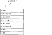
- FIG. 2 is a schematic view showing the layer structure of another embodiment of the organic EL device of the present invention.
- the organic EL element 2 is an example of a hybrid type organic EL element in which a phosphorescent light emitting layer and a fluorescent light emitting layer are laminated.
- the organic EL element 2 has the same configuration as the organic EL element 1 except that a space layer 42 and a fluorescent light emitting layer 44 are formed between the phosphorescent light emitting layer 40 and the electron transport zone 50.
- the excitons formed in the phosphorescent light emitting layer 40 are not diffused into the fluorescent light emitting layer 44, so that a space layer 42 is provided between the fluorescent light emitting layer 44 and the phosphorescent light emitting layer 40. May be provided. Since the material of the present invention has a large triplet energy, it can function as a space layer.
- a white light emitting organic EL element can be obtained by setting the phosphorescent light emitting layer to emit yellow light and the fluorescent light emitting layer to blue light emitting layer.
- the phosphorescent light-emitting layer and the fluorescent light-emitting layer are formed one by one.
- the present invention is not limited to this, and two or more layers may be formed, and can be appropriately set according to the application such as lighting and display device.
- a full color light emitting device is formed using a white light emitting element and a color filter
- a plurality of wavelength regions such as red, green, blue (RGB), red, green, blue, yellow (RGBY) are used from the viewpoint of color rendering. In some cases, it may be preferable to include luminescence.
- the organic EL element of the present invention can employ various known configurations. Further, light emission of the light emitting layer can be taken out from the anode side, the cathode side, or both sides. In the organic EL element of this invention, it is not specifically limited about structures other than the layer which uses the organic EL element material of this invention mentioned above, A well-known material etc. can be used. Hereinafter, although the layer of the element of Embodiment 1 is demonstrated easily, the material applied to the organic EL element of this invention is not limited to the following.
- a glass plate, a polymer plate or the like can be used as the substrate.
- the glass plate include soda lime glass, barium / strontium-containing glass, lead glass, aluminosilicate glass, borosilicate glass, barium borosilicate glass, and quartz.
- the polymer plate include polycarbonate, acrylic, polyethylene terephthalate, polyether sulfone, and polysulfone.
- the anode is made of, for example, a conductive material, and a conductive material having a work function larger than 4 eV is suitable.
- the conductive material include carbon, aluminum, vanadium, iron, cobalt, nickel, tungsten, silver, gold, platinum, palladium, and their alloys, ITO substrate, tin oxide used for NESA substrate, indium oxide, and the like.
- examples thereof include metal oxides and organic conductive resins such as polythiophene and polypyrrole.
- the anode may be formed with a layer structure of two or more layers if necessary.
- the cathode is made of, for example, a conductive material, and a conductive material having a work function smaller than 4 eV is suitable.
- the conductive material include, but are not limited to, magnesium, calcium, tin, lead, titanium, yttrium, lithium, ruthenium, manganese, aluminum, lithium fluoride, and alloys thereof.
- the alloy include magnesium / silver, magnesium / indium, lithium / aluminum, and the like, but are not limited thereto.
- the ratio of the alloy is controlled by the temperature of the vapor deposition source, the atmosphere, the degree of vacuum, etc., and is selected to an appropriate ratio.
- the cathode may be formed with a layer structure of two or more layers, and the cathode can be produced by forming a thin film from the conductive material by a method such as vapor deposition or sputtering.
- the transmittance of the cathode for light emission is preferably greater than 10%.
- the sheet resistance as the cathode is preferably several hundred ⁇ / ⁇ or less, and the film thickness is usually 10 nm to 1 ⁇ m, preferably 50 to 200 nm.
- the phosphorescent light emitting layer is formed of a material other than the organic EL element material of the present invention
- a known material can be used as the material of the phosphorescent light emitting layer.
- International Publication No. 2005/079118 Japanese Patent Application No. 2005-517938
- the organic EL device of the present invention may have a fluorescent light emitting layer like the device shown in FIG.
- a known material can be used for the fluorescent light emitting layer.
- the light emitting layer may be a double host (also referred to as a host / cohost). Specifically, the carrier balance in the light emitting layer may be adjusted by combining an electron transporting host and a hole transporting host in the light emitting layer. Moreover, it is good also as a double dopant.
- each dopant emits light by adding two or more dopant materials having a high quantum yield. For example, a yellow light emitting layer may be realized by co-evaporating a host, a red dopant, and a green dopant.
- the light emitting layer may be a single layer or a laminated structure. When the light emitting layer is stacked, the recombination region can be concentrated on the light emitting layer interface by accumulating electrons and holes at the light emitting layer interface. This improves the quantum efficiency.
- the hole injection / transport layer is a layer that assists hole injection into the light emitting layer and transports it to the light emitting region, and has a high hole mobility and a small ionization energy of usually 5.6 eV or less.
- As the material for the hole injection / transport layer a material that transports holes to the light emitting layer with lower electric field strength is preferable. Further, when an electric field is applied with a hole mobility of, for example, 10 4 to 10 6 V / cm, At least 10 ⁇ 4 cm 2 / V ⁇ sec is preferable.
- the material for the hole injection / transport layer include triazole derivatives (see US Pat. No. 3,112,197) and oxadiazole derivatives (see US Pat. No. 3,189,447). ), Imidazole derivatives (see JP-B-37-16096, etc.), polyarylalkane derivatives (US Pat. Nos. 3,615,402, 3,820,989, 3,542,544) Nos. 45-555, 51-10983, 51-93224, 55-17105, 56-4148, 55-108667, 55-156953, 56-36656, etc.), pyrazoline derivatives and pyrazolone derivatives (US Pat. Nos. 3,180,729, 4th) Nos.
- Gazette 55-52063, 55-52064, 55-46760, 57-11350, 57- No. 148749, JP-A-2-311591, etc.), stilbene derivatives (JP-A Nos. 61-210363, 61-228451, 61-14642, 61-72255, etc.) 62-47646, 62-36684, 62-10652, 62-30255, 60-93455, 60-94462, 60-174749, 60 -175052, etc.), silazane derivatives (US Pat. No. 4,950,950), polysilanes (JP-A-2-204996), aniline copolymers (JP-A-2-282263) Etc.
- inorganic compounds such as p-type Si and p-type SiC can also be used as the hole injection material.
- a cross-linkable material can be used as the material of the hole injection / transport layer.
- a cross-linkable material for example, Chem. Mater. 2008, 20, 413-422, Chem. Mater. 2011, 23 (3), 658-681, International Publication No. 2008/108430, International Publication No. 2009/102027, International Publication No. 2009/123269, International Publication No. 2010/016555, National Publication No. 2010/018813.
- the layer which insolubilized the crosslinking material described in No. etc. by heat, light, etc. is mentioned.
- the electron injection / transport layer is a layer that assists the injection of electrons into the light emitting layer and transports it to the light emitting region, and has a high electron mobility.
- an electrode for example, a cathode
- the electron injecting / transporting layer is appropriately selected with a film thickness of several nm to several ⁇ m.
- the electron mobility is preferably at least 10 ⁇ 5 cm 2 / Vs or more when an electric field of V / cm is applied.
- an aromatic heterocyclic compound containing one or more heteroatoms in the molecule is preferably used, and a nitrogen-containing ring derivative is particularly preferable.
- the nitrogen-containing ring derivative is preferably an aromatic ring having a nitrogen-containing 6-membered ring or 5-membered ring skeleton, or a condensed aromatic ring compound having a nitrogen-containing 6-membered ring or 5-membered ring skeleton, such as a pyridine ring. , Pyrimidine ring, triazine ring, benzimidazole ring, phenanthroline ring, quinazoline ring and the like.
- an organic layer having semiconductivity may be formed by doping (n) with a donor material and doping (p) with an acceptor material.
- N doping is to dope a metal such as Li or Cs into an electron transporting material
- P doping is to dope an acceptor material such as F4TCNQ into a hole transporting material ( For example, refer patent 3695714).
- the organic EL device of the present invention preferably has at least one of an electron donating dopant and an organometallic complex in an interface region between the cathode and the organic thin film layer. According to such a configuration, it is possible to improve the light emission luminance and extend the life of the organic EL element.
- the electron donating dopant include at least one selected from alkali metals, alkali metal compounds, alkaline earth metals, alkaline earth metal compounds, rare earth metals, rare earth metal compounds, and the like.
- the organometallic complex include at least one selected from an organometallic complex containing an alkali metal, an organometallic complex containing an alkaline earth metal, an organometallic complex containing a rare earth metal, and the like.
- alkali metal examples include lithium (Li) (work function: 2.93 eV), sodium (Na) (work function: 2.36 eV), potassium (K) (work function: 2.28 eV), rubidium (Rb) (work Function: 2.16 eV), cesium (Cs) (work function: 1.95 eV) and the like, and those having a work function of 2.9 eV or less are particularly preferable.
- K, Rb, and Cs are preferred, Rb and Cs are more preferred, and Cs is most preferred.
- alkaline earth metal examples include calcium (Ca) (work function: 2.9 eV), strontium (Sr) (work function: 2.0 eV to 2.5 eV), barium (Ba) (work function: 2.52 eV).
- a work function of 2.9 eV or less is particularly preferable.
- the rare earth metal examples include scandium (Sc), yttrium (Y), cerium (Ce), terbium (Tb), ytterbium (Yb) and the like, and those having a work function of 2.9 eV or less are particularly preferable.
- preferred metals are particularly high in reducing ability, and by adding a relatively small amount to the electron injection region, it is possible to improve the light emission luminance and extend the life of the organic EL element.
- alkali metal compound examples include lithium oxide (Li 2 O), cesium oxide (Cs 2 O), alkali oxides such as potassium oxide (K 2 O), lithium fluoride (LiF), sodium fluoride (NaF), fluorine.
- alkali halides such as cesium fluoride (CsF) and potassium fluoride (KF), and lithium fluoride (LiF), lithium oxide (Li 2 O), and sodium fluoride (NaF) are preferable.
- alkaline earth metal compound examples include barium oxide (BaO), strontium oxide (SrO), calcium oxide (CaO), and barium strontium oxide (Ba x Sr 1-x O) (0 ⁇ x ⁇ 1), Examples thereof include barium calcium oxide (Ba x Ca 1-x O) (0 ⁇ x ⁇ 1), and BaO, SrO, and CaO are preferable.
- the rare earth metal compound ytterbium fluoride (YbF 3), scandium fluoride (ScF 3), scandium oxide (ScO 3), yttrium oxide (Y 2 O 3), cerium oxide (Ce 2 O 3), gadolinium fluoride (GdF 3), include such terbium fluoride (TbF 3) is, YbF 3, ScF 3, TbF 3 are preferable.
- the organometallic complex is not particularly limited as long as it contains at least one of an alkali metal ion, an alkaline earth metal ion, and a rare earth metal ion as a metal ion as described above.
- the ligands include quinolinol, benzoquinolinol, acridinol, phenanthridinol, hydroxyphenyloxazole, hydroxyphenylthiazole, hydroxydiaryloxadiazole, hydroxydiarylthiadiazole, hydroxyphenylpyridine, hydroxyphenylbenzimidazole, hydroxybenzotriazole, Hydroxyfulborane, bipyridyl, phenanthroline, phthalocyanine, porphyrin, cyclopentadiene, ⁇ -diketones, azomethines, and derivatives thereof are preferred, but are not limited thereto.
- the electron donating dopant and the organometallic complex it is preferable to form a layer or an island in the interface region.
- a forming method while depositing at least one of an electron donating dopant and an organometallic complex by a resistance heating vapor deposition method, an organic material as a light emitting material or an electron injection material for forming an interface region is simultaneously deposited, and an electron is deposited in the organic material.
- a method of dispersing at least one of a donor dopant and an organometallic complex reducing dopant is preferable.
- the dispersion concentration is usually organic substance: electron donating dopant and / or organometallic complex in a molar ratio of 100: 1 to 1: 100, preferably 5: 1 to 1: 5.
- the electron donating dopant and the organometallic complex is formed in a layered form
- the light emitting material or the electron injecting material which is the organic layer at the interface is formed in a layered form
- at least one of the electron donating dopant and the organometallic complex is formed.
- These are vapor-deposited by resistance heating vapor deposition method alone, and preferably the layer thickness is 0.1 nm or more and 15 nm or less.
- the electron donating dopant and the organometallic complex is formed in an island shape
- the electron donating dopant and the organometallic complex At least one of them is vapor-deposited by resistance heating vapor deposition, and the island is preferably formed with a thickness of 0.05 nm to 1 nm.
- the ratio of at least one of the main component (light-emitting material or electron injection material), the electron-donating dopant, and the organometallic complex is, as a molar ratio, the main component: the electron-donating dopant.
- / or organometallic complex 5: 1 to 1: 5, preferably 2: 1 to 1: 2.
- each layer of the organic EL device of the present invention a known method such as a dry film forming method such as vacuum deposition, sputtering, plasma, or ion plating, or a wet film forming method such as spin coating, dipping, or flow coating is applied. be able to.
- the thickness of each layer is not particularly limited, but must be set to an appropriate thickness. If the film thickness is too thick, a large applied voltage is required to obtain a constant light output, resulting in poor efficiency. If the film thickness is too thin, pinholes and the like are generated, and sufficient light emission luminance cannot be obtained even when an electric field is applied.
- the normal film thickness is suitably in the range of 5 nm to 10 ⁇ m, but more preferably in the range of 10 nm to 0.2 ⁇ m.
- Example 1 A 25 mm ⁇ 75 mm ⁇ 1.1 mm glass substrate with an ITO transparent electrode (manufactured by Geomatic) was subjected to ultrasonic cleaning for 5 minutes in isopropyl alcohol, and further subjected to UV (Ultraviolet) ozone cleaning for 30 minutes. .
- the glass substrate with the transparent electrode thus cleaned is attached to the substrate holder of the vacuum evaporation apparatus, and first, on the surface of the glass substrate on which the transparent electrode line is formed, the transparent electrode is covered, Material 1 was deposited with a thickness of 20 nm to obtain a hole injection layer. Subsequently, the material 2 was vapor-deposited with a thickness of 60 nm on this film to obtain a hole transport layer.
- compound 1 as a phosphorescent host material and material 3 which is a phosphorescent material were co-evaporated at a thickness of 50 nm to obtain a phosphorescent layer.
- concentration of Compound 1 in the phosphorescent light emitting layer was 80% by mass, and the concentration of Material 3 was 20% by mass.
- the material 5 was deposited on the phosphorescent layer at a thickness of 10 nm to obtain a hole blocking layer. Furthermore, after depositing material 4 with a thickness of 10 nm to obtain an electron transport layer, LiF with a thickness of 1 nm and metal Al with a thickness of 80 nm were sequentially laminated to obtain a cathode. Note that LiF, which is an electron injecting electrode, was formed at a rate of 1 ⁇ / min.
- Example 2 to 9 An organic EL device was prepared and evaluated in the same manner as in Example 1 except that the compounds shown in Table 1 below were used in place of Compound 1 as the phosphorescent host material. The results are shown in Table 1.
- Example 10 An organic EL device was prepared in the same manner as in Example 1 except that Compound 2 was used instead of the hole blocking layer material 5 of Example 1 and that the host material of the light emitting layer and the material 5 instead of Compound 1 were used. ,evaluated. The results of Example 10 are shown in Table 2 together with Example 1. [Examples 11 and 12] An organic EL device was prepared and evaluated in the same manner as in Example 1 except that the compounds shown in Table 2 were used in place of the hole blocking layer material 5 of Example 1. The results of Examples 11 to 12 are shown in Table 2. [Reference Example 1] An organic EL device was prepared and evaluated in the same manner as in Example 1 except that Comparative Compound 1 was used in place of the material 5 for the hole blocking layer of Example 1.
- Reference Example 1 The results of Reference Example 1 are shown in Table 2.
- Reference Example 2 An organic EL device was prepared and evaluated in the same manner as in Example 10 except that Comparative Compound 2 was used instead of Compound 2 in the hole blocking layer of Example 10. The results of Reference Example 2 are shown in Table 2.
- the organic EL device of the present invention can be used for a flat light emitter such as a flat panel display of a wall-mounted television, a light source such as a copying machine, a printer, a backlight of a liquid crystal display or instruments, a display board, a marker lamp, and the like.
- the compound of the present invention can be used for organic EL devices, organic EL displays, lighting, organic semiconductors, organic solar cells, and the like.
- the organic EL device material of the present invention is useful as an organic EL device that can be driven at a low voltage and has high efficiency and a long lifetime, and an organic EL device material that realizes the organic EL device.
Landscapes
- Chemical & Material Sciences (AREA)
- Organic Chemistry (AREA)
- Engineering & Computer Science (AREA)
- Materials Engineering (AREA)
- Physics & Mathematics (AREA)
- Spectroscopy & Molecular Physics (AREA)
- Electroluminescent Light Sources (AREA)
Abstract
Cette invention concerne le composé de formule (1).
Applications Claiming Priority (2)
| Application Number | Priority Date | Filing Date | Title |
|---|---|---|---|
| JP2012-000636 | 2012-01-05 | ||
| JP2012000636 | 2012-01-05 |
Publications (1)
| Publication Number | Publication Date |
|---|---|
| WO2013102992A1 true WO2013102992A1 (fr) | 2013-07-11 |
Family
ID=48745068
Family Applications (1)
| Application Number | Title | Priority Date | Filing Date |
|---|---|---|---|
| PCT/JP2012/008429 Ceased WO2013102992A1 (fr) | 2012-01-05 | 2012-12-28 | Matériau pour élément organique électroluminescent et élément utilisant ce matériau |
Country Status (2)
| Country | Link |
|---|---|
| TW (1) | TW201343639A (fr) |
| WO (1) | WO2013102992A1 (fr) |
Cited By (14)
| Publication number | Priority date | Publication date | Assignee | Title |
|---|---|---|---|---|
| JP2015122459A (ja) * | 2013-12-25 | 2015-07-02 | 三星ディスプレイ株式會社Samsung Display Co.,Ltd. | 有機el素子 |
| EP2910555A1 (fr) * | 2014-02-24 | 2015-08-26 | Universal Display Corporation | Matériaux et dispositifs électroluminescents organiques |
| WO2015156235A1 (fr) * | 2014-04-09 | 2015-10-15 | 住友化学株式会社 | Élément électroluminescent et composition utilisée dedans |
| KR20160052677A (ko) * | 2013-09-05 | 2016-05-12 | 바이엘 크롭사이언스 악티엔게젤샤프트 | N-벤질-n-시클로프로필-1h-피라졸-4-카르복사미드 유도체의 합성 절차 |
| CN106661006A (zh) * | 2014-07-29 | 2017-05-10 | 默克专利有限公司 | 用于有机电致发光器件的材料 |
| JPWO2016052337A1 (ja) * | 2014-09-30 | 2017-07-20 | 住友化学株式会社 | 発光素子 |
| US9755159B2 (en) | 2014-01-23 | 2017-09-05 | Universal Display Corporation | Organic materials for OLEDs |
| WO2018025554A1 (fr) * | 2016-08-02 | 2018-02-08 | コニカミノルタ株式会社 | Procédé de production d'un composé hétérocyclique contenant de l'azote |
| KR20180074582A (ko) * | 2016-12-23 | 2018-07-03 | 가부시키가이샤 한도오따이 에네루기 켄큐쇼 | 유기 화합물, 발광 소자, 발광 장치, 전자 기기, 및 조명 장치 |
| WO2019143112A1 (fr) * | 2018-01-16 | 2019-07-25 | 주식회사 두산 | Dispositif électroluminescent organique |
| KR20200030479A (ko) * | 2018-09-12 | 2020-03-20 | 주식회사 엘지화학 | 화합물 및 이를 포함하는 유기 발광 소자 |
| WO2020208475A1 (fr) * | 2019-04-12 | 2020-10-15 | 株式会社半導体エネルギー研究所 | Composé organique, dispositif électroluminescent, appareil électroluminescent, dispositif électronique et appareil d'éclairage |
| JP2021005714A (ja) * | 2013-07-16 | 2021-01-14 | ユニバーサル ディスプレイ コーポレイション | カルバゾール含有化合物 |
| CN116813599A (zh) * | 2022-03-18 | 2023-09-29 | 北京夏禾科技有限公司 | 有机电致发光材料及其器件 |
Families Citing this family (1)
| Publication number | Priority date | Publication date | Assignee | Title |
|---|---|---|---|---|
| CN109734648A (zh) * | 2018-11-29 | 2019-05-10 | 宇瑞(上海)化学有限公司 | 有机电致器件用化合物及其使用该化合物的有机电致器件 |
Citations (8)
| Publication number | Priority date | Publication date | Assignee | Title |
|---|---|---|---|---|
| WO2007119816A1 (fr) * | 2006-04-19 | 2007-10-25 | Konica Minolta Holdings, Inc. | Matériau pour élément électroluminescent organique, élément électroluminescent organique, dispositif d'affichage et appareil d'éclairage |
| WO2009060780A1 (fr) * | 2007-11-08 | 2009-05-14 | Konica Minolta Holdings, Inc. | Elément électroluminescent organique, dispositif d'affichage, et système d'éclairage |
| WO2009104488A1 (fr) * | 2008-02-20 | 2009-08-27 | コニカミノルタホールディングス株式会社 | Dispositif électroluminescent organique émettant de la lumière blanche |
| JP2011084531A (ja) * | 2009-10-19 | 2011-04-28 | Konica Minolta Holdings Inc | 有機エレクトロルミネッセンス素子用材料、有機エレクトロルミネッセンス素子、照明装置及び表示装置 |
| WO2011125680A1 (fr) * | 2010-03-31 | 2011-10-13 | 出光興産株式会社 | Matériau pour élément électroluminescent organique, et élément électroluminescent organique utilisant ce matériau |
| WO2011137072A1 (fr) * | 2010-04-26 | 2011-11-03 | Universal Display Corporation | Composés contenant un bicarbazole pour oled |
| WO2012023947A1 (fr) * | 2010-08-20 | 2012-02-23 | Universal Display Corporation | Composés de bicarbazole pour dispositifs électroluminescents organiques (oled) |
| WO2012108389A1 (fr) * | 2011-02-07 | 2012-08-16 | 出光興産株式会社 | Dérivé de bis-carbazole ainsi qu'élément électroluminescent organique mettant en oeuvre celui-ci |
-
2012
- 2012-12-28 WO PCT/JP2012/008429 patent/WO2013102992A1/fr not_active Ceased
-
2013
- 2013-01-03 TW TW102100101A patent/TW201343639A/zh unknown
Patent Citations (8)
| Publication number | Priority date | Publication date | Assignee | Title |
|---|---|---|---|---|
| WO2007119816A1 (fr) * | 2006-04-19 | 2007-10-25 | Konica Minolta Holdings, Inc. | Matériau pour élément électroluminescent organique, élément électroluminescent organique, dispositif d'affichage et appareil d'éclairage |
| WO2009060780A1 (fr) * | 2007-11-08 | 2009-05-14 | Konica Minolta Holdings, Inc. | Elément électroluminescent organique, dispositif d'affichage, et système d'éclairage |
| WO2009104488A1 (fr) * | 2008-02-20 | 2009-08-27 | コニカミノルタホールディングス株式会社 | Dispositif électroluminescent organique émettant de la lumière blanche |
| JP2011084531A (ja) * | 2009-10-19 | 2011-04-28 | Konica Minolta Holdings Inc | 有機エレクトロルミネッセンス素子用材料、有機エレクトロルミネッセンス素子、照明装置及び表示装置 |
| WO2011125680A1 (fr) * | 2010-03-31 | 2011-10-13 | 出光興産株式会社 | Matériau pour élément électroluminescent organique, et élément électroluminescent organique utilisant ce matériau |
| WO2011137072A1 (fr) * | 2010-04-26 | 2011-11-03 | Universal Display Corporation | Composés contenant un bicarbazole pour oled |
| WO2012023947A1 (fr) * | 2010-08-20 | 2012-02-23 | Universal Display Corporation | Composés de bicarbazole pour dispositifs électroluminescents organiques (oled) |
| WO2012108389A1 (fr) * | 2011-02-07 | 2012-08-16 | 出光興産株式会社 | Dérivé de bis-carbazole ainsi qu'élément électroluminescent organique mettant en oeuvre celui-ci |
Cited By (40)
| Publication number | Priority date | Publication date | Assignee | Title |
|---|---|---|---|---|
| JP2021005714A (ja) * | 2013-07-16 | 2021-01-14 | ユニバーサル ディスプレイ コーポレイション | カルバゾール含有化合物 |
| JP7015353B2 (ja) | 2013-07-16 | 2022-02-02 | ユニバーサル ディスプレイ コーポレイション | カルバゾール含有化合物 |
| KR20160052677A (ko) * | 2013-09-05 | 2016-05-12 | 바이엘 크롭사이언스 악티엔게젤샤프트 | N-벤질-n-시클로프로필-1h-피라졸-4-카르복사미드 유도체의 합성 절차 |
| KR102254277B1 (ko) | 2013-09-05 | 2021-05-20 | 바이엘 크롭사이언스 악티엔게젤샤프트 | N-벤질-n-시클로프로필-1h-피라졸-4-카르복사미드 유도체의 합성 절차 |
| JP2015122459A (ja) * | 2013-12-25 | 2015-07-02 | 三星ディスプレイ株式會社Samsung Display Co.,Ltd. | 有機el素子 |
| US9755159B2 (en) | 2014-01-23 | 2017-09-05 | Universal Display Corporation | Organic materials for OLEDs |
| EP2910555A1 (fr) * | 2014-02-24 | 2015-08-26 | Universal Display Corporation | Matériaux et dispositifs électroluminescents organiques |
| KR20150100555A (ko) * | 2014-02-24 | 2015-09-02 | 유니버셜 디스플레이 코포레이션 | 유기 전계발광 물질 및 소자 |
| JP2015157808A (ja) * | 2014-02-24 | 2015-09-03 | ユニバーサル ディスプレイ コーポレイション | 有機エレクトロルミネセンス材料、及びデバイス |
| US9502656B2 (en) | 2014-02-24 | 2016-11-22 | Universal Display Corporation | Organic electroluminescent materials and devices |
| KR102254064B1 (ko) | 2014-02-24 | 2021-05-20 | 유니버셜 디스플레이 코포레이션 | 유기 전계발광 물질 및 소자 |
| WO2015156235A1 (fr) * | 2014-04-09 | 2015-10-15 | 住友化学株式会社 | Élément électroluminescent et composition utilisée dedans |
| EP3131131A4 (fr) * | 2014-04-09 | 2017-11-08 | Sumitomo Chemical Company Limited | Élément électroluminescent et composition utilisée dedans |
| JPWO2015156235A1 (ja) * | 2014-04-09 | 2017-04-13 | 住友化学株式会社 | 発光素子およびそれに用いる組成物 |
| CN106133938B (zh) * | 2014-04-09 | 2018-06-19 | 住友化学株式会社 | 发光元件和用于该发光元件的组合物 |
| CN106133938A (zh) * | 2014-04-09 | 2016-11-16 | 住友化学株式会社 | 发光元件和用于该发光元件的组合物 |
| US11309497B2 (en) | 2014-07-29 | 2022-04-19 | Merck Patent Gmbh | Materials for organic electroluminescent devices |
| CN106661006A (zh) * | 2014-07-29 | 2017-05-10 | 默克专利有限公司 | 用于有机电致发光器件的材料 |
| CN106661006B (zh) * | 2014-07-29 | 2019-11-08 | 默克专利有限公司 | 用于有机电致发光器件的材料 |
| JPWO2016052337A1 (ja) * | 2014-09-30 | 2017-07-20 | 住友化学株式会社 | 発光素子 |
| EP3203543A4 (fr) * | 2014-09-30 | 2018-06-06 | Sumitomo Chemical Company Limited | Élément électroluminescent |
| CN107078223B (zh) * | 2014-09-30 | 2019-03-29 | 住友化学株式会社 | 发光元件 |
| CN107078223A (zh) * | 2014-09-30 | 2017-08-18 | 住友化学株式会社 | 发光元件 |
| JP7179614B2 (ja) | 2016-08-02 | 2022-11-29 | メルク パテント ゲーエムベーハー | 含窒素複素環化合物の製造方法 |
| WO2018025554A1 (fr) * | 2016-08-02 | 2018-02-08 | コニカミノルタ株式会社 | Procédé de production d'un composé hétérocyclique contenant de l'azote |
| JPWO2018025554A1 (ja) * | 2016-08-02 | 2019-05-30 | コニカミノルタ株式会社 | 含窒素複素環化合物の製造方法 |
| JP2018104413A (ja) * | 2016-12-23 | 2018-07-05 | 株式会社半導体エネルギー研究所 | 有機化合物、発光素子、発光装置、電子機器、及び照明装置 |
| KR20180074582A (ko) * | 2016-12-23 | 2018-07-03 | 가부시키가이샤 한도오따이 에네루기 켄큐쇼 | 유기 화합물, 발광 소자, 발광 장치, 전자 기기, 및 조명 장치 |
| JP7330322B2 (ja) | 2016-12-23 | 2023-08-21 | 株式会社半導体エネルギー研究所 | 有機化合物及び発光素子 |
| KR102616441B1 (ko) * | 2016-12-23 | 2023-12-26 | 가부시키가이샤 한도오따이 에네루기 켄큐쇼 | 유기 화합물, 발광 소자, 발광 장치, 전자 기기, 및 조명 장치 |
| JP2022079492A (ja) * | 2016-12-23 | 2022-05-26 | 株式会社半導体エネルギー研究所 | 有機化合物及び発光素子 |
| WO2019143112A1 (fr) * | 2018-01-16 | 2019-07-25 | 주식회사 두산 | Dispositif électroluminescent organique |
| KR102232411B1 (ko) | 2018-09-12 | 2021-03-26 | 주식회사 엘지화학 | 화합물 및 이를 포함하는 유기 발광 소자 |
| KR20200030479A (ko) * | 2018-09-12 | 2020-03-20 | 주식회사 엘지화학 | 화합물 및 이를 포함하는 유기 발광 소자 |
| JPWO2020208475A1 (fr) * | 2019-04-12 | 2020-10-15 | ||
| WO2020208475A1 (fr) * | 2019-04-12 | 2020-10-15 | 株式会社半導体エネルギー研究所 | Composé organique, dispositif électroluminescent, appareil électroluminescent, dispositif électronique et appareil d'éclairage |
| JP7531481B2 (ja) | 2019-04-12 | 2024-08-09 | 株式会社半導体エネルギー研究所 | 有機化合物、発光デバイス、発光装置、電子機器、および照明装置 |
| US12364159B2 (en) | 2019-04-12 | 2025-07-15 | Semiconductor Energy Laboratory Co., Ltd. | Organic compound, light-emitting device, light-emitting apparatus, electronic device, and lighting device |
| KR102943367B1 (ko) | 2019-04-12 | 2026-03-24 | 가부시키가이샤 한도오따이 에네루기 켄큐쇼 | 유기 화합물, 발광 디바이스, 발광 장치, 전자 기기, 및 조명 장치 |
| CN116813599A (zh) * | 2022-03-18 | 2023-09-29 | 北京夏禾科技有限公司 | 有机电致发光材料及其器件 |
Also Published As
| Publication number | Publication date |
|---|---|
| TW201343639A (zh) | 2013-11-01 |
Similar Documents
| Publication | Publication Date | Title |
|---|---|---|
| JP6012611B2 (ja) | 有機エレクトロルミネッセンス素子用材料及びそれを用いた有機エレクトロルミネッセンス素子 | |
| JP6148982B2 (ja) | 含窒素へテロ芳香族環化合物 | |
| JP6212391B2 (ja) | 有機エレクトロルミネッセンス素子 | |
| US9685614B2 (en) | Material for organic electroluminescent element, and element using same | |
| WO2013102992A1 (fr) | Matériau pour élément organique électroluminescent et élément utilisant ce matériau | |
| JP6220341B2 (ja) | ラダー化合物、及びそれを用いた有機エレクトロルミネッセンス素子 | |
| CN102471320A (zh) | 含芴芳香族化合物、有机电致发光元件用材料及使用其的有机电致发光元件 | |
| US20150034927A1 (en) | Material for organic electroluminescent element, and organic electroluminescent element using same | |
| WO2013175746A1 (fr) | Élément électroluminescent organique | |
| WO2012018120A1 (fr) | Dérivé de monoamine et élément électroluminescent organique l'utilisant | |
| JPWO2013069242A1 (ja) | 有機エレクトロルミネッセンス素子用材料及びそれを用いた有機エレクトロルミネッセンス素子 | |
| JP2013108015A (ja) | 有機エレクトロルミネッセンス素子用材料 | |
| JPWO2013108589A1 (ja) | 新規化合物、有機エレクトロルミネッセンス素子用材料及び有機エレクトロルミネッセンス素子 | |
| JP6031302B2 (ja) | ヘテロ芳香族化合物及びそれを用いた有機エレクトロルミネッセンス素子 | |
| US9496508B2 (en) | Material for organic electroluminescent element and organic electroluminescent element using same | |
| WO2014112359A1 (fr) | Élément électroluminescent organique |
Legal Events
| Date | Code | Title | Description |
|---|---|---|---|
| 121 | Ep: the epo has been informed by wipo that ep was designated in this application |
Ref document number: 12864224 Country of ref document: EP Kind code of ref document: A1 |
|
| NENP | Non-entry into the national phase |
Ref country code: DE |
|
| 122 | Ep: pct application non-entry in european phase |
Ref document number: 12864224 Country of ref document: EP Kind code of ref document: A1 |
|
| NENP | Non-entry into the national phase |
Ref country code: JP |