WO2013105574A1 - Dispositif à microcanaux et procédé de fabrication de celui-ci - Google Patents
Dispositif à microcanaux et procédé de fabrication de celui-ci Download PDFInfo
- Publication number
- WO2013105574A1 WO2013105574A1 PCT/JP2013/050194 JP2013050194W WO2013105574A1 WO 2013105574 A1 WO2013105574 A1 WO 2013105574A1 JP 2013050194 W JP2013050194 W JP 2013050194W WO 2013105574 A1 WO2013105574 A1 WO 2013105574A1
- Authority
- WO
- WIPO (PCT)
- Prior art keywords
- substrate
- channel
- bonding
- self
- groove
- Prior art date
- Legal status (The legal status is an assumption and is not a legal conclusion. Google has not performed a legal analysis and makes no representation as to the accuracy of the status listed.)
- Ceased
Links
Images


Classifications
-
- B—PERFORMING OPERATIONS; TRANSPORTING
- B81—MICROSTRUCTURAL TECHNOLOGY
- B81C—PROCESSES OR APPARATUS SPECIALLY ADAPTED FOR THE MANUFACTURE OR TREATMENT OF MICROSTRUCTURAL DEVICES OR SYSTEMS
- B81C1/00—Manufacture or treatment of devices or systems in or on a substrate
- B81C1/00015—Manufacture or treatment of devices or systems in or on a substrate for manufacturing microsystems
- B81C1/00023—Manufacture or treatment of devices or systems in or on a substrate for manufacturing microsystems without movable or flexible elements
- B81C1/00119—Arrangement of basic structures like cavities or channels, e.g. suitable for microfluidic systems
-
- B—PERFORMING OPERATIONS; TRANSPORTING
- B01—PHYSICAL OR CHEMICAL PROCESSES OR APPARATUS IN GENERAL
- B01J—CHEMICAL OR PHYSICAL PROCESSES, e.g. CATALYSIS OR COLLOID CHEMISTRY; THEIR RELEVANT APPARATUS
- B01J19/00—Chemical, physical or physico-chemical processes in general; Their relevant apparatus
- B01J19/0093—Microreactors, e.g. miniaturised or microfabricated reactors
-
- B—PERFORMING OPERATIONS; TRANSPORTING
- B01—PHYSICAL OR CHEMICAL PROCESSES OR APPARATUS IN GENERAL
- B01L—CHEMICAL OR PHYSICAL LABORATORY APPARATUS FOR GENERAL USE
- B01L3/00—Containers or dishes for laboratory use, e.g. laboratory glassware; Droppers
- B01L3/50—Containers for the purpose of retaining a material to be analysed, e.g. test tubes
- B01L3/502—Containers for the purpose of retaining a material to be analysed, e.g. test tubes with fluid transport, e.g. in multi-compartment structures
- B01L3/5027—Containers for the purpose of retaining a material to be analysed, e.g. test tubes with fluid transport, e.g. in multi-compartment structures by integrated microfluidic structures, i.e. dimensions of channels and chambers are such that surface tension forces are important, e.g. lab-on-a-chip
- B01L3/502707—Containers for the purpose of retaining a material to be analysed, e.g. test tubes with fluid transport, e.g. in multi-compartment structures by integrated microfluidic structures, i.e. dimensions of channels and chambers are such that surface tension forces are important, e.g. lab-on-a-chip characterised by the manufacture of the container or its components
-
- B—PERFORMING OPERATIONS; TRANSPORTING
- B01—PHYSICAL OR CHEMICAL PROCESSES OR APPARATUS IN GENERAL
- B01J—CHEMICAL OR PHYSICAL PROCESSES, e.g. CATALYSIS OR COLLOID CHEMISTRY; THEIR RELEVANT APPARATUS
- B01J2219/00—Chemical, physical or physico-chemical processes in general; Their relevant apparatus
- B01J2219/00002—Chemical plants
- B01J2219/00004—Scale aspects
- B01J2219/00006—Large-scale industrial plants
-
- B—PERFORMING OPERATIONS; TRANSPORTING
- B01—PHYSICAL OR CHEMICAL PROCESSES OR APPARATUS IN GENERAL
- B01J—CHEMICAL OR PHYSICAL PROCESSES, e.g. CATALYSIS OR COLLOID CHEMISTRY; THEIR RELEVANT APPARATUS
- B01J2219/00—Chemical, physical or physico-chemical processes in general; Their relevant apparatus
- B01J2219/00781—Aspects relating to microreactors
- B01J2219/00925—Irradiation
- B01J2219/0093—Electric or magnetic energy
-
- B—PERFORMING OPERATIONS; TRANSPORTING
- B01—PHYSICAL OR CHEMICAL PROCESSES OR APPARATUS IN GENERAL
- B01L—CHEMICAL OR PHYSICAL LABORATORY APPARATUS FOR GENERAL USE
- B01L2300/00—Additional constructional details
- B01L2300/06—Auxiliary integrated devices, integrated components
- B01L2300/0627—Sensor or part of a sensor is integrated
- B01L2300/0645—Electrodes
-
- B—PERFORMING OPERATIONS; TRANSPORTING
- B01—PHYSICAL OR CHEMICAL PROCESSES OR APPARATUS IN GENERAL
- B01L—CHEMICAL OR PHYSICAL LABORATORY APPARATUS FOR GENERAL USE
- B01L2300/00—Additional constructional details
- B01L2300/08—Geometry, shape and general structure
- B01L2300/0809—Geometry, shape and general structure rectangular shaped
- B01L2300/0816—Cards, e.g. flat sample carriers usually with flow in two horizontal directions
-
- B—PERFORMING OPERATIONS; TRANSPORTING
- B01—PHYSICAL OR CHEMICAL PROCESSES OR APPARATUS IN GENERAL
- B01L—CHEMICAL OR PHYSICAL LABORATORY APPARATUS FOR GENERAL USE
- B01L2300/00—Additional constructional details
- B01L2300/08—Geometry, shape and general structure
- B01L2300/0861—Configuration of multiple channels and/or chambers in a single devices
- B01L2300/0867—Multiple inlets and one sample wells, e.g. mixing, dilution
-
- B—PERFORMING OPERATIONS; TRANSPORTING
- B01—PHYSICAL OR CHEMICAL PROCESSES OR APPARATUS IN GENERAL
- B01L—CHEMICAL OR PHYSICAL LABORATORY APPARATUS FOR GENERAL USE
- B01L2300/00—Additional constructional details
- B01L2300/08—Geometry, shape and general structure
- B01L2300/0861—Configuration of multiple channels and/or chambers in a single devices
- B01L2300/0883—Serpentine channels
-
- B—PERFORMING OPERATIONS; TRANSPORTING
- B01—PHYSICAL OR CHEMICAL PROCESSES OR APPARATUS IN GENERAL
- B01L—CHEMICAL OR PHYSICAL LABORATORY APPARATUS FOR GENERAL USE
- B01L2300/00—Additional constructional details
- B01L2300/08—Geometry, shape and general structure
- B01L2300/0887—Laminated structure
-
- B—PERFORMING OPERATIONS; TRANSPORTING
- B81—MICROSTRUCTURAL TECHNOLOGY
- B81B—MICROSTRUCTURAL DEVICES OR SYSTEMS, e.g. MICROMECHANICAL DEVICES
- B81B2201/00—Specific applications of microelectromechanical systems
- B81B2201/05—Microfluidics
- B81B2201/058—Microfluidics not provided for in B81B2201/051 - B81B2201/054
Definitions
- the present invention relates to a microchannel device and a method for manufacturing the microchannel device, and is suitable for application to, for example, a microchannel device having a hollow channel space between a first substrate and a second substrate.
- micro Electro Mechanical Systems Micro Electro Mechanical Systems
- flow structures, pumps, valves, mixers, and other microstructures are integrated on several centimeter square substrates, and fluids are sent and mixed to analyze fluids.
- ⁇ TAS Micro Total Analysis Systems
- an electrode-embedded microchannel device in which an electrode is provided in the channel space is also being considered for higher functionality of the device, and a method for manufacturing this type of electrode-embedded microchannel device Research is also underway.
- a microchannel device is manufactured by joining a concave substrate formed with a concave groove to be a channel or a chamber and a flat cover substrate. Manufacturing methods are known.
- the concave substrate and the cover substrate are irradiated with vacuum plasma or vacuum ultraviolet rays by an excimer UV lamp
- a manufacturing method is known in which oxygen-containing groups are introduced into each bonding surface of the concave substrate and the cover substrate, and the bonding surfaces are bonded and thermocompression bonded together to react and bond oxygen-containing groups (for example, Patent Document 1 and Non-Patent Document 1).
- the bonding method by introducing the oxygen-containing group is not limited to the above-described method, and for example, UV ozone treatment using a low-pressure mercury lamp, atmospheric pressure plasma treatment, or the like may be used.
- Non-Patent Document 2 a self-assembled monomolecular film (SAM film) is formed on a concave substrate and a cover substrate, and terminal functional groups of the self-assembled monomolecular film are bonded to each other.
- a bonding method is also known in which the concave substrate and the cover substrate are bonded by chemical reaction.
- the present invention has been made in consideration of the above points, and can maintain the desired characteristics of the flow path space, and can prevent a defect caused by joining the flow path groove of the first substrate and the second substrate. It aims at proposing a channel device and its manufacturing method.
- claim 1 of the present invention has a flow channel groove serving as a flow channel space on the joint surface, and the first self-organizing unit is selectively formed only on the joint surface excluding the flow channel groove.
- a first substrate on which a molecular film is formed; and a second substrate on which a second self-assembled monomolecular film is formed on a bonding facing surface facing the bonding surface of the first substrate, the first self-organization The first functional group of the first monolayer and the second functional group of the second self-assembled monolayer are bonded to each other, and the first substrate and the second substrate are joined together.
- a microchannel device characterized in that a hollow channel space is formed therebetween.
- a dummy member forming step of forming a dummy member in the flow channel groove provided on the bonding surface of the first substrate and protecting the flow channel groove with the dummy member; and the bonding of the first substrate Forming a first self-assembled monolayer on the surface and the dummy member; and removing the dummy member and selectively forming the first self-assembled surface only on the joint surface excluding the flow channel
- a terminal functional group with a monomolecular film is bonded, the first substrate and the second substrate are joined, and a hollow channel space is formed between the first substrate and the second substrate by the channel groove.
- a microchannel device comprising a bonding step It is a method of manufacture.
- the first self-assembled monolayer is not formed in the flow channel, the wettability in the flow channel, surface free energy, surface functional groups, etc.
- the characteristics of the material of the channel groove itself can be maintained in the channel space without changing the characteristics, and the second substrate can be reliably bonded only by the bonding surface excluding the channel groove.
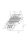
- FIG. 1 indicates a light-emitting device using the micro-channel device 2 of the present invention, and this light-emitting device 1 is connected to the micro-channel device 2 via wiring 4
- the power supply 5 is connected.
- a plurality of first electrodes 11a, 11b, 11c and a plurality of second electrodes 18a, 18b, 18c are provided in the microchannel device 2, and these first electrodes 11a, 11b, 11c and the second electrodes 18a, 18b, and 18c are individually provided with power via wiring.
- a common power supply 5 is connected to only one first electrode 11b and second electrode 18b via wiring 4, and the other first electrodes 11a, 11c and second electrodes are connected.
- the power supply connected to 18a and 18c is omitted.
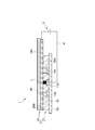
- the entire microchannel device 2 is formed in a flat shape, and a channel space 14 is formed therein.
- the width of the channel space 14 is selected to be about 10 to 2000 [ ⁇ m], the depth is about 10 to 200 [mm], and the thickness (distance between electrodes) is about 1 to 100 [ ⁇ m].
- a first substrate 7 provided with a plurality of first electrodes 11a, 11b, 11c and a second substrate 8 provided with a plurality of second electrodes 18a, 18b, 18c are joined.
- a hollow channel space 14 is formed between the first substrate 7 and the second substrate 8.
- the first substrate 7 has a configuration in which the channel forming layer 12 is provided on the support substrate 10, and the channel space 14 is formed in the channel forming layer 12.
- a flow path space 14 is surrounded by the support substrate 10, the flow path forming layer 12, and the second substrate 8.
- the microchannel device 2 is formed with a plurality of (in this case, three) channel spaces 14 having the same configuration, and a luminescent liquid is respectively contained in each channel space 14. It is configured to flow.
- a plurality of channel spaces 14 formed in a straight line are arranged so that the longitudinal directions thereof are parallel to each other.
- Each flow path space 14 has an inlet 2a formed at one end and an outlet 2b formed at the other end.
- tube members (not shown) are provided at the inlet 2a and the outlet 2b, respectively. Can be connected.
- the luminescent liquid is supplied to the channel space 14 from the inlet 2a at one end by the upstream tube member, the microchannel device 2 passes through the channel space 14 and flows at the other end.
- the luminescent liquid flows out from the outlet 2b to the tube member on the downstream side, and different luminescent liquids can flow into the respective flow path spaces 14.
- the luminescent liquid mentioned above refers to a form in which a luminescent compound is added to various solvents, liquid semiconductors, ionic liquids, or a mixed solution thereof.
- the light emitting compound is preferably a light emitter of an organic compound.
- the various solvents used are water, methanol, ethanol, 1-propanol, 2-propanol, tetrahydrofuran, 1,4-dioxane, acetone, 4-methyl-2-pentanone, acetylacetone, acetonitrile, propionitrile, ethylenediamine, pyridine.
- Formamide N-methylpyrrolidone, dimethyl sulfoxide, sulfolane, nitromethane, nitrobenzene, 1,2-dichlorobenzene, chloroform, methylene chloride, dichloromethane, 1,2-dichloroethane, propylene carbonate, ethylene carbonate, acetic acid, acetic anhydride, toluene, Examples include xylene, mesitylene, tetralin, decalin, n-butylbenzene, and benzonitrile.
- a liquid semiconductor refers to a state of a liquid organic semiconductor, for example, aromatic hydrocarbons such as a benzene derivative, a naphthalene derivative, an anthracene derivative, a carbazole derivative, and a typical one is 9- (2-ethylhexyl) carbazole (EHCz ) Or PLQ.
- the ionic liquid is an ionic liquid that is liquid at room temperature (25 ° C.), and a configuration represented by the general formula AB (A is a cation and B is an anion) is a good example.
- Examples of the cation represented by A above include the following. N, N, N-trimethylbutylammonium ion, N-ethyl-N, N-dimethylpropylammonium ion, N-ethyl-N, N-dimethylbutylammonium ion, N, N-dimethyl-N-propylbutylammonium ion, N- (2-methoxyethyl) -N, N-dimethylethylammonium ion, 1-ethyl-3-methylimidazolium ion, 1-ethyl-2,3-dimethylimidazolium ion, 1-ethyl-3,4- Dimethylimidazolium ion, 1-ethyl-2,3,4-trimethylimidazolium ion, 1-ethyl-2,3,5-trimethylimidazolium ion, N-methyl-N-propylpyrrolidinium ion, N
- N-methyl-N-propylpiperidinium ions are particularly preferred as the cation because of the wide potential window used.
- examples of the anion represented by B include PF 6 ⁇ , [PF 3 (C 2 F 5 ) 3 ] ⁇ , [PF 3 (CF 3 ) 3 ] ⁇ , BF 4 ⁇ , [BF 2 (CF 3) 2] -, [BF 2 (C 2 F 5) 2] -, [BF 3 (CF 3)] -, [BF 3 (C 2 F 5)] -, (BOB -), [(CF 3 SO 2 ) 2 N] ⁇ (TFSI ⁇ ), [(C 2 F 5 SO 2 ) 2 N] ⁇ (BETI ⁇ ), [(CF 3 SO 2 ) (C 4 F 9 SO 2 ) N] ⁇ , [ (CN) 2 N] ⁇ (DCA ⁇ ), [(CF 3 SO 2 ) 3 C] ⁇ , [(CN) 3 C] ⁇ and the anion
- BF 4 ⁇ [BF 3 (CF 3 )] ⁇ , [BF 3 (C 2 F 5 )] ⁇ , BOB ⁇ , TFSI ⁇ and BETI ⁇ are preferable.
- the addition amount of the luminescent substance is preferably 1 to 99% by weight, more preferably 5 to 90% by weight, with respect to various solvents, liquid semiconductors, ionic liquids or mixed solutions thereof.
- FIG. 2A is a schematic diagram for explaining the light emission principle when a liquid semiconductor is used as the luminescent liquid L.
- FIG. 2A a voltage is applied to the first electrode 11b and the second electrode 18b by the power source 5, and in this state, the flow path between the first electrode 11b and the second electrode 18b.
- the luminescent liquid L flows into the space 14
- holes are injected from the first electrode 11b into the luminescent liquid L, and electrons are flown into the luminescent liquid L from the second electrode 18b.
- the holes and electrons in L recombine with each other, and the excitons generated thereby can emit light when returning to the ground state.
- FIG. 2B is a schematic diagram for explaining the light emission principle by the ECL.
- a voltage is applied to the first electrode 11b and the second electrode 18b by the power source 5, and the channel space 14 between the first electrode 11b and the second electrode 18b is applied.
- the cation radical R + generated at the first electrode 11b serving as the anode and the anion radical R ⁇ generated at the second electrode 18b serving as the cathode are contained in the luminescent liquid L. And neutral molecules in the ground state and excited state are generated, and the neutral molecules in the excited state can emit light when returning to the ground state.
- the luminescent liquid L constantly or intermittently flows in the flow path space 14 from the inlet 2a toward the outlet 2b, and the luminescent liquid L deteriorated in the flow path space 14.
- the new luminescent liquid L continues to be supplied to the flow path space 14 without being stopped, so that the optimum light emission state can be maintained for a long time.
- the second substrate 8 is disposed on the channel forming layer 12 of the first substrate 7, and the support substrate 10 and the channel forming layer 12 are sequentially arranged from the bottom.
- the second substrate 8 is laminated.
- the support substrate 10 constituting the first substrate 7 is made of various materials such as glass, polyester (PET (polyethylene terephthalate), PEN (polyethylene naphthalate)), polycarbonate, polyimide resin, acrylic resin member, and the like.
- the outer shape is formed in a plate shape or a sheet shape in a quadrilateral shape, and one surface on which the flow path forming layer 12 is laminated is formed flat.
- the light emitting state of the luminescent liquid L flowing in the channel space 14 is visually recognized from the outside on the first substrate 7 side by forming the support substrate 10 with various transparent materials. Can do.
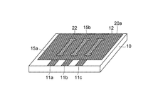
- first electrodes 11a, 11b, and 11c are arranged on one surface of the support substrate 10 so as to run in parallel with each other in the longitudinal direction.
- the flow path forming layer 12 can be laminated so that the hole 15 faces the first electrodes 11a, 11b, and 11c.
- the first electrodes 11a, 11b, and 11c of the support substrate 10 are exposed in the groove forming through holes 15 of the flow path forming layer 12 on the first substrate 7, and the groove forming through holes 15 and the first electrodes 11a, 11a,
- a channel groove having a concave cross section can be formed by 11b and 11c.
- the first electrodes 11a, 11b, and 11c can be formed of a transparent electrode such as ITO, IZO, or ZnO, a metal such as gold, platinum, silver, magnesium, lithium, or aluminum, or an alloy thereof.
- the flow path forming layer 12 is formed of, for example, a negative photosensitive resin, and is formed so that a quadrilateral outline dimension is within the frame of the support substrate 10, and the longitudinal direction is substantially parallel to the longitudinal direction of the support substrate 10. Is provided.
- the flow path forming layer 12 is provided with circular diameter-enlarged regions 15a and 15b communicating with the inflow port 2a and the outflow port 2b, respectively, at both ends of the groove-forming through hole 15 formed in a band shape.
- the diameter-enlarged regions 15a and 15b can also be arranged to face the first electrodes 11a, 11b, and 11c on the support substrate 10.
- the first self-assembled monolayer 21a is selectively formed on the bonding surface 20a of the flow path forming layer 12 facing the second substrate 8 except for the flow path grooves. Is formed.
- the first substrate 7 has the second self formed on the bonding facing surface 20b of the second substrate 8 on the terminal functional group of the first self-assembled monolayer 21a on the bonding surface 20a facing the second substrate 8.
- the terminal functional group of the organized monolayer 21b is bonded, and the second substrate 8 can be bonded.
- the first self-assembled monolayer 21a is preferably composed of a self-assembled monomolecule having an epoxy as a terminal functional group.
- a self-assembled monomolecule having an epoxy as a terminal functional group For example, 3-glycidyloxypropyltrimethoxysilane (GOPTS, GPTS, GPTMS ), 3-glycidoxypropyltriethoxysilane (GPTES), 3-glycidoxypropylmethyldiethoxysilane (GPMDES), 3-glycidoxypropylmethyldimethoxysilane and the like.
- the second self-assembled monolayer 21b that binds to the terminal functional group of the first self-assembled monolayer 21a may be composed of a self-assembled monomolecule having —NH 2 as the terminal functional group.
- APTES 3-aminopropyltriethoxysilane
- APITMS 3-aminopropyltrimethoxysilane
- N-2- (aminoethyl) -3-aminopropylmethyldimethoxysilane N-2- (aminoethyl) -3-aminopropyltrimethoxysilane
- N-2- (aminoethyl) -3-aminopropyltriethoxysilane N-2- (aminoethyl) -3-aminopropyltriethoxysilane, and the like.
- a self-assembled monomolecular film having epoxy as a terminal functional group is formed on the first substrate 7 as the first self-assembled monomolecular film 21a, and —NH 2 is formed as the terminal functional group.
- the present invention is not limited to this.
- a self-assembled monomolecular film having a second self-assembled monomolecular film on the second substrate 8 and a self-assembled monomolecular film having —NH 2 as a terminal functional group as the first self-assembled monomolecular film May be formed on the first substrate 7.
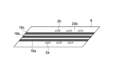
- the second substrate 8 on which such second self-assembled monolayer 21b is formed is, for example, polyester (PET (polyethylene terephthalate) or PEN (polyethylene naphthalate)), polycarbonate, polyimide resin, acrylic resin member. It is made of various film-like or sheet-like materials, and its outer shape is formed in a quadrilateral shape, and a joining facing surface 20b joined to the joining surface 20a of the first substrate 7 is formed almost flat.
- the second substrate 8 is formed of various transparent materials, so that the light emission state of the luminescent liquid L flowing in the channel space 14 can be changed from the outside on the second substrate 8 side. Visible.
- a plurality of strip-shaped second electrodes 18a, 18b, 18c are arranged on the joint facing surface 20b of the second substrate 8 so as to run in parallel in the longitudinal direction. These second electrodes 18a, 18b, 18c
- the first substrate 7 may be disposed so that the longitudinal direction of the first substrate 7 is orthogonal to the longitudinal direction of the flow channel grooves of the first substrate 7 (that is, the first electrodes 11a, 11b, 11c).
- a channel space 14 in which, for example, the first electrode 11b and a part of the second electrode 18b face each other can be formed between the first substrate 7 and the second substrate 8.
- the second electrodes 18a, 18b, and 18c are made of, for example, transparent electrodes such as ITO, IZO, and ZnO, as well as the first electrodes 11a, 11b, and 11c, as well as gold, platinum, silver, magnesium, lithium, and aluminum.
- the second substrate 8 is provided with a plurality of inlets 2a and outlets 2b penetrating the thickness at predetermined positions around the second electrodes 18a, 18b, 18c.
- the second substrate 8 is positioned on the flow path forming layer 12 so that the inlet 2a and the outlet 2b overlap with the enlarged diameter regions 15a and 15b of the flow path forming layer 12, and is joined to the flow path forming layer 12. obtain.
- the support substrate 10 and the second substrate are formed of a soft member such as polyester (PET), and the first electrodes 11a, 11b, 11c and the second electrodes 18a, 18b,
- a soft electrode member such as ITO
- ITO a soft electrode member such as ITO
- the longitudinal direction of the second electrodes 18a, 18b, 18c on the second substrate 8 is the longitudinal direction of the first electrodes 11a, 11b, 11c on the first substrate 7.
- the one end of the first substrate 7 protrudes from the side of the second substrate 8 and the one end of the second substrate 8 protrudes from the side of the first substrate 7. It has a configuration.
- the microchannel device 2 can expose the first electrodes 11a, 11b, 11c at one end of the first substrate 7 without overlapping the second substrate 8, and accordingly, the first electrodes 11a, 11b. , 11c can be easily connected to the wiring 4.
- the wiring 4 is connected to the second electrodes 18a, 18b, and 18c accordingly. It can be easily connected.
- the micro-channel device 2 having such a configuration is selected only for the joining surface 20a except for the channel groove of the first substrate 7, as shown in FIG. 4 showing a side cross-sectional configuration of the AA ′ portion of FIG.
- Terminal functional groups of the first self-assembled monolayer formed on the second substrate 8 and the second self-assembled monolayer on the bonding facing surface 20b of the second substrate 8 are bonded to each other.
- the substrate 8 is joined, the channel groove is not bonded to the second substrate 8, the hollow channel space 14 can be reliably formed, and the characteristics of the channel space are not changed.
- the characteristics of the first electrode 11a, 11b, 11c, the flow path forming layer 12, the second electrode 18a, 18b, 18c, and the second substrate 8 can be maintained.
- the luminescent liquid L can be surely passed through the channel space 14, and the first electrode 11a, 11b, 11c and the second electrode 18a, 18b, 18c are supplied by the power source 5.
- the luminescent liquid L flowing through the flow path space 14 can be caused to emit light.
- a manufacturing method of such a microchannel device 2 will be described below.
- a plate-like support substrate having an electrode layer formed on the surface is prepared, and the electrode layer on the support substrate is etched with a resin mask pattern, and as shown in FIG. Shaped first electrodes 11a, 11b, and 11c are formed.
- a negative photosensitive resin is spin-coated on the support substrate 10 on which the first electrodes 11a, 11b, and 11c are formed, and the negative photosensitive resin is heated and prebaked.
- a belt-shaped groove-forming through-hole region 22 having enlarged diameter regions 15a and 15b at both ends can be exposed using a mask (not shown) using an exposure apparatus for performing photolithography. Solubilize.
- post-exposure baking is performed at a predetermined temperature, development is performed with a developer, and the solubilized groove-forming through-hole region 22 is removed to form the groove-forming through-hole 15 in the negative photosensitive resin.
- Post-baking is performed at a temperature, and a flow path forming layer 12 in which the first electrodes 11a, 11b, and 11c are exposed at the bottom of the groove forming through hole 15 is formed on the support substrate 10 (not shown).
- the flow path forming layer 12 is preferably formed of the above-described negative photosensitive resin since it is desired that the height and width of the flow path groove can be easily changed.
- SU manufactured by Microchem (Nippon Kayaku) -8 series, KMPR series, Tokyo Ohka Kogyo TMMR S2000, Toray Photo Nice (photosensitive polyimide), etc. are used.
- a dummy member such as a dummy resin (TSMR: manufactured by Tokyo Ohka Kogyo Co., Ltd.) is prepared, and the dummy member 23a is formed in the groove forming through hole 15 of the flow path forming layer 12 as shown in FIG. And then baked at a predetermined temperature. In this way, the entire inside of the channel groove 23 is covered with the dummy member 23a, and the first electrodes 11a, 11b, 11c in the channel groove 23 are not exposed to the outside.
- TSMR dummy resin
- the dummy member 23a for example, the TSMR series manufactured by Tokyo Ohka Kogyo, which is a positive resist that dissolves in an organic solvent (acetone or the like), the OFPR series, the AZ series manufactured by Clariant, or the like may be used.
- the dummy member 23a when the channel groove width is 500 [un] or larger, the dummy member 23a may be provided directly in the channel groove by directly tracing the dummy member 23a with a syringe or the like.
- the dummy member 23a when the flow path width is narrow, after the dummy member 23a is spin-coated on the substrate 10, the dummy member 23a is formed by exposing and developing a portion other than the portion where the dummy member is to be formed using a mask.
- the flow channel groove is covered with a plate-like member provided with a supply port and a discharge port, and the dummy member 23a is fed from the supply port through the flow channel groove to the dummy member 23a.
- the member 23a may be provided, and then the plate member may be removed to form the dummy member 23a only in the flow channel.
- a film-like second substrate having an electrode layer formed on the surface is prepared, and the electrode layer on the second substrate is etched with a resin mask pattern, and as shown in FIG.
- Second electrodes 18a, 18b and 18c having a predetermined shape are formed on the two substrates 8 from electrode layers.
- the second substrate 8 has through-holes having substantially the same shape and size as the enlarged diameter regions 15a and 15b at positions corresponding to the enlarged diameter regions 15a and 15b of the groove-forming through-holes 15 of the flow path forming layer 12.
- a hole is formed by punching to form an inlet 2a and an outlet 2b.
- the second substrate 8 is manufactured in which the second electrodes 18a, 18b, and 18c are provided on the bonding facing surface 20b, and the inflow port 2a and the outflow port 2b are formed.
- the excimer UV is applied to the bonding surface 20a provided with the dummy member 23a of the first substrate 7 and the bonding facing surface 20b provided with the second electrode 18b of the second substrate 8.
- the lamp is irradiated with vacuum ultraviolet light (VUV / O 3 ), and oxygen-containing groups (carboxyl groups, ketones) are formed on the dummy member 23a and the bonding surface 20a of the first substrate 7 and the bonding facing surface 20b of the second substrate 8, respectively.
- oxygen-containing groups carboxyl groups, ketones
- UV / O 3 treatment using a low-pressure mercury lamp, atmospheric pressure plasma treatment, Vacuum plasma treatment or the like may be used.
- first substrate is immersed in a first self-assembled monomolecular formation solution (first SAM formation solution), and as shown in FIG. 10A, on the bonding surface 20a of the first substrate 7 and the dummy member 23a, For example, a first self-assembled monolayer 21a having a terminal functional group made of epoxy such as 3-glycidyloxypropyltrimethoxysilane (GOPTS) is formed.
- first substrate 7 is rinsed with a removing solution such as acetone, and the residual self-assembled monomolecules that are not attached to the bonding surface 20a and the dummy member 23a in the channel groove 23 are removed.
- a removing solution such as acetone
- the first electrode 11a, 11b, 11c is exposed on the bottom of the flow channel 23 on the first substrate 7, and the first self-organization is selectively performed only on the bonding surface 20a excluding the flow channel 23.
- a monomolecular film 21a can be formed.
- the second substrate 8 is immersed in a second self-assembled monomolecular formation solution (second SAM formation solution), and as shown in FIG. 10B, on the bonding facing surface 20b of the second substrate 8, for example, 3- A second self-assembled monolayer 21b whose terminal functional group is an amino group, such as aminopropyltriethoxysilane (APTES), is formed.
- second substrate 8 is rinsed with ethanol or the like to remove residual self-assembled monomolecules that are not attached to the bonding facing surface 20b.
- the second substrate 8 includes the second self-assembled monomolecule on the entire bonding facing surface 20b other than the second electrodes 18a, 18b, 18c, including the exposed second electrodes 18a, 18b, 18c.
- the film 21b can be formed.
- the first substrate 7 whose surface 20a is modified by the first self-assembled monolayer 21a and the second surface 20b whose surface 20b is modified by the second self-assembled monolayer 21b.
- the substrate 8 is brought into contact, and the first substrate 7 and the second substrate 8 are loaded and heated in this state, and as shown in FIG. 11, the terminal functional groups of the first self-assembled monolayer 21a and the first functional group 2
- the terminal functional group of the self-assembled monomolecular film 21b is bonded by an epoxy-amino reaction.
- the first self-assembled monolayer 21a is formed. Since the entire flow channel groove 23 that was not formed was white, it was confirmed that the hollow flow channel space 14 could be reliably formed without the entire flow channel groove 23 being bonded to the second substrate 8. .
- the second substrate 8 has a slightly concavity and convexity on the bonding facing surface 20b on which the second electrodes 18a, 18b, and 18c are provided depending on the presence or absence of the second electrodes 18a, 18b, and 18c.
- the first self-assembled monolayer 21a of the first substrate 7 and the second self-assembled monolayer 21b of the bonding facing surface 20b are formed of a deformable film-like member. Therefore, the bonding facing surface 20b is brought into close contact with the bonding surface 20a of the first substrate 7 so that the bonding can be reliably performed.
- the first substrate 7 and the second substrate 8 are closely bonded without forming a gap, and the channel space 14 that communicates with the outside only through the inlet 2 a and the outlet 2 b is formed.
- the first substrate 7 and the second substrate 8 can be formed.
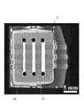
- the microchannel device 2 was actually manufactured according to the above manufacturing method, and a light-emitting device 1 using this micro-channel device 2 In FIG. 5, the verification was made on how the luminescent liquid L emits light in the flow path space.
- the microchannel device 2 was manufactured as follows. First, an ITO-glass substrate was prepared in which a supporting substrate 10 was a 700 [ ⁇ m] thick glass substrate on which 100 [nm] thick ITO was formed on one surface. Next, a resin mask pattern was formed on the ITO using a positive photosensitive resin TSMR manufactured by Tokyo Ohka Kogyo Co., Ltd.
- the support substrate 10 formed so that the three first electrodes 11a, 11b, and 11c having a strip shape as shown in FIG.
- a negative photosensitive resin (SU-8 3005: manufactured by Nippon Kayaku Co., Ltd.) with excellent chemical resistance and mechanical properties is spin-coated to a thickness of 6 [ ⁇ m], and this negative photosensitive resin is hot.
- a mask aligner MA6: manufactured by Carlsose
- the exposure was carried out at [mW / cm 2 ] for 6 seconds to solubilize the groove-forming through-hole region 22 as shown in FIG.
- the flow path forming layer 12 with the first electrodes 11a, 11b, and 11c exposed at the bottom of the groove forming through hole 15 is further hard-baked at 150 [° C.]. It was formed on the support substrate 10.
- a resin material made of TSMR (manufactured by Tokyo Ohka Kogyo Co., Ltd.) is prepared as a dummy member 23a, and as shown in FIG. 7, this TSMR is injected into the groove forming through-hole 15 of the flow path forming layer 12, and hot The plate was baked at 110 [° C.] for 5 minutes. In this way, the entire inside of the channel groove 23 is covered with the dummy member 23a, and the first electrodes 11a, 11b, 11c in the channel groove 23 are not exposed to the outside. In this state, vacuum ultraviolet light ( VUV / O 3 ) was irradiated to form oxygen-containing groups on the flow path forming layer 12 and the dummy member 23a.
- VUV / O 3 vacuum ultraviolet light
- first SAM formation solution a 1% (v / v) 3-glycidyloxypropyltrimethoxysilane (GOPTS) solution dissolved in pure water is prepared as a first self-assembled monomolecular formation solution (first SAM formation solution) to form a first SAM.
- first SAM formation solution a first self-assembled monomolecular formation solution
- the first substrate 7 is immersed in the solution for 20 minutes, and a first self-assembled monolayer 21a in which GOPTS having a terminal functional group made of epoxy is provided on the bonding surface 20a of the first substrate 7 and the dummy member 23a as a film. Formed.
- the first substrate 7 is rinsed with acetone to cover the remaining self-assembled monomolecules not attached to the bonding surface 20a and the flow channel 23.
- the dummy member 23a was removed, and then rinsed with isopropyl alcohol and pure water to remove acetone.
- the first electrodes 11a, 11b, 11c are exposed at the bottom of the flow channel 23, and the first self-assembled monolayer 21a is selectively formed only on the bonding surface 20a excluding the flow channel 23.
- a first substrate 7 was manufactured.
- an ITO-PEN film in which ITO having a thickness of 350 [nm] was formed on a PEN film having a thickness of 120 [ ⁇ m] was prepared as the second substrate 8.
- the ITO on the second substrate 8 was etched with a resin mask pattern, and as shown in FIG. 8, three second electrodes 18a, 18b, 18c having a strip shape were formed from the ITO.
- a through hole having substantially the same shape and size as the enlarged diameter regions 15 a, 15 b is provided at a position corresponding to the enlarged diameter regions 15 a, 15 b of the groove forming through hole 15 in the flow path forming layer 12. Were punched to form the inlet 2a and the outlet 2b.
- the second substrate 8 in which the second electrodes 18a, 18b, and 18c were provided on the bonding facing surface 20b and the inflow port 2a and the outflow port 2b were formed was manufactured.
- the junction facing surface 20b of the second substrate 8 was also irradiated with vacuum ultraviolet light (VUV / O 3 ) by an excimer UV lamp to form an oxygen-containing group on the junction facing surface 20b.
- VUV / O 3 vacuum ultraviolet light
- APTES 3-aminopropyltriethoxysilane
- second SAM formation solution a second self-assembled monomolecular formation solution
- the second substrate 8 was immersed in the solution for 20 minutes to form a second self-assembled monolayer 21b in which the APTES whose terminal functional group is an amino group was provided on the bonding facing surface 20b of the second substrate 8 as a film.
- the second substrate 8 is lifted from the second SAM forming solution, the second substrate 8 is rinsed with ethanol to remove residual self-assembled monomolecules not attached to the bonding facing surface 20b, and thus exposed.
- a second substrate 8 was produced in which the second self-assembled monolayer 21b was formed on the bonding facing surface 20b including the second electrodes 18a, 18b and 18c.
- first self-assembled monolayer 21a of the first substrate 7 and the second self-assembled monolayer 21b of the second substrate 8 are brought into contact with each other, and the bonding apparatus (EVG520HE: EV group, Inc.) remains in this state.
- the first self-assembled monolayer 21a and the second self-assembled monolayer 21b are bonded to each other by applying a load with a load of 1.5 [MPa], a temperature of 140 [° C] and a holding time of 5 minutes.
- the substrate 7 and the second substrate 8 were joined, and the microchannel device 2 including the three channel spaces 14 having widths of 1000 [ ⁇ m], 1250 [ ⁇ m], and 1500 [ ⁇ m] was manufactured.
- the fixing device 41 includes a first plastic plate 52 erected on a base 51 and a second plastic plate 53 that is a separate body from the first plastic plate 52.
- the micro-channel device 2 was made visible through the glass windows 57 and 58 embedded in the first plastic plate 52 and the second plastic plate 53 with the device 2 interposed therebetween.
- the first plastic plate 52 is provided with a pin member 55a penetrating the thickness, and one end of the pin member 55a exposed on one surface is brought into contact with the second electrodes 18a, 18b, 18c of the microchannel device 2 and exposed on the other surface.
- the wiring 4 (FIG. 13) is connected to the other end of the pin member 55a so that the voltage from the power supply device 43 can be applied to the second electrodes 18a, 18b, and 18c via the wiring 4 and the pin member 55a.
- the second plastic plate 53 is provided with a pin member 55b penetrating the thickness, and one end of the pin member 55b exposed on one surface is brought into contact with the first electrodes 11a, 11b, 11c of the microchannel device 2, and the other surface
- the wiring 4 (FIG. 13) is connected to the other end of the pin member 55b exposed to the voltage so that the voltage from the power supply device 43 can be applied to the first electrodes 11a, 11b, and 11c via the wiring 4 and the pin member 55b. did.
- the second plastic plate 53 is provided with openings communicating with the inlet 2a and the outlet 2b of the microchannel device 2, and a sealing pin 56 or a connecting pipe 56a (FIG. 13) is provided in the opening. It was.
- the cylinder 44 is connected to the inlet 2a communicating with the channel space 14 to be verified in the microchannel device 2 via the connection pipe 56a, and the cylinder 44 is connected to the inlet 2a via the inlet 2a.
- the luminescent liquid L was supplied to the channel space 14. Note that the luminescent liquid L supplied to the flow path space 14 is retained in the flow path space 14 by the sealing pin 56 provided at the outlet 2b of the micro flow path device 2.
- UV is irradiated to the microchannel device 2 using the UV lamp 45, and the light emission state of the luminescent liquid L supplied into the channel space 14 of the microchannel device 2 is imaged by the digital camera 46.
- a liquid semiconductor is injected as the luminescent liquid L into the channel space 14 located in the center among the three channel spaces 14 of the microchannel device 2 to correspond to the channel space 14.
- a voltage was applied to the central first electrode 11b and the three second electrodes 18a, 18b, 18c orthogonal to the first electrode 11b. As a result, a result as shown in FIG. 15A was obtained.
- the microfluidic device 2 manufactured by the manufacturing method described above, the first electrode 11b and the second electrodes 18a, 18b, at 18c is opposed, centrally disposed hollow flow path space 14b 1 It was confirmed that the luminescent liquid L emitted light. In addition, it was confirmed that in the flow path space 14b 1 , it was possible to prevent defects due to the joining of the flow path grooves of the first substrate 7 and the second substrate 8.
- rubrene ((5,6,11,12) -tetraphenyltetracene) that emits yellow light is mixed into a mixed solvent (2: 1, v / v) of 1,2 dichlorobenzene and acetonitrile.
- DBP Dissolved luminescent solution
- DBP-rubrene solution Dissolved luminescent solution
- a luminescent compound doped with rubrene mixed solvent of 1,2 dichlorobenzene and acetonitrile (2: 1, v / v )
- a luminescent solution hereinafter simply referred to as a DBP-rubrene solution
- the rubrene solution is allowed to flow through the channel space 14a 1 on one end side and the DBP-rubrene in the channel space 14c 1 on the other end side
- the solution was allowed to flow, and voltages were applied to the three second electrodes 18a, 18b, 18c orthogonal to the first electrode 11b.
- FIG. 15B a result as shown in FIG. 15B was obtained.
- the hollow channel space 14a 1 arranged on one end side is turned yellow by a rubden solution (indicated simply as “rubrene” in FIG. 15B).
- the hollow channel space 14c 1 arranged on the other end side can be made to emit red light with a DBP-rubrene solution (indicated simply as “DBP” in FIG. 15B). did it.
- DBP DBP-rubrene solution
- DPA 9,10-diphenylanthracene
- a luminescent solution dissolved in v) (hereinafter simply referred to as a DPA solution) is prepared, and this DPA solution is allowed to flow only in the central flow path space 14b 1 and three second electrodes 18a, Voltage was applied to 18b and 18c.
- a result as shown in FIG. 15C was obtained. From FIG. 15C, in the microchannel device 2 manufactured by the above-described manufacturing method, the blue channel space 14b 1 disposed in the center emits blue light by the DPA solution (simply expressed as “DPA” in FIG. 15C). I was able to.
- the concentration of rubrene in the rubrene solution is preferably 1 to 20 [mM], and the concentrations of rubrene and DBP used in the DBP-rubrene solution are preferably 1 to 20 [mM] and 0.1 to 0.4 [mM], respectively.
- the concentration of DPA is preferably 5 to 50 [mM].
- non-patent literature "K. Nishimura etal., Solution Electrochemiluminescent Cell with a High Luminance Using an Ion Conductive Assistant Dopant '', Japanese Journal of Applied Physics (Jpn. J. Appl. Phys), vol. pp. L 1323-L 1326, .2001 ”is added to the luminescent liquid as an ion conductive auxiliary dopant (0.122M of 1,2 diphenoxyethane).
- the luminescent liquid L is changed, and the rubrene solution that emits yellow light again as the luminescent liquid L is caused to flow through the channel space 14a 1 on one end side and the channel space 14c 1 on the other end side, and the first electrode.
- a voltage was applied to the three second electrodes 18a, 18b, and 18c orthogonal to 11b.
- FIG. 15D a result as shown in FIG. 15D was obtained.
- the rubrene solution is passed through the hollow channel space 14a 1 disposed on one end side and the hollow channel space 14c 1 disposed on the other end side.
- each channel space 14a 1 to 14c 1 can simultaneously emit yellow light, and even if the luminescent liquid L is changed, each channel space 14a 1 to 14c 1 emits light without causing poor bonding. I was able to.
- each channel space 14a 1 to 14c 1 can be caused to emit light using not only a liquid semiconductor but also various luminescent liquids L, and light emission It was confirmed that each flow path space 14a 1 to 14c 1 can emit light even when the type of the ionic liquid L is changed.
- the first self-assembled monolayer 21a is selectively formed only on the bonding surface 20a excluding the channel groove 23 of the first substrate 7. Then, the terminal functional group of the second self-assembled monolayer 21b formed on the bonding facing surface 20b of the second substrate 8 and the terminal functional group of the first self-assembled monolayer 21a are bonded to each other. The first substrate 7 and the second substrate 8 are joined together to form a hollow flow path space 14 between the first substrate 7 and the second substrate 8.
- the first self-assembled monolayer 21a is not formed in the channel groove 23 since the first self-assembled monolayer 21a is not formed in the channel groove 23, characteristics such as wettability, surface free energy, surface functional groups, etc. of the channel groove 23 are obtained.
- the characteristics of the material of the flow channel 23 itself can be maintained without change, and the first substrate can be reliably bonded to the second substrate 8 only by the bonding surface 20a excluding the flow channel 23. It is possible to prevent defects caused by joining the seven flow path grooves and the second substrate 8.
- the first electrodes 11a, 11b, and 11c are formed so as to be exposed in the channel groove 23, and the first electrodes 11a, 11b, and 11b are formed on the bonding facing surface 20b of the second substrate 8.
- Second electrodes 18a, 18b, 18c that are at least partially opposed to 11c are provided, and these first electrodes 11a, 11b, 11c and second electrodes 18a, 18b, 18c are arranged to face each other across channel space 14 I tried to do it.
- the microchannel device 2 by applying a voltage to the first electrodes 11a, 11b, 11c and the second electrodes 18a, 18b, 18c, the first electrodes 11a, 11b, 11c and the second electrodes 18a, the first electrodes 11a, 11b, 11c and the second electrodes 18a, The luminescent liquid L flowing in the flow path space 14 between 18b and 18c can emit light.
- the luminescent liquid L can be supplied from the inflow port 2a to the channel space 14 by providing the inflow port 2a and the outflow port 2b for communicating the channel space 14 with the outside.
- the luminescent liquid L supplied to the flow path space 14 can flow out from the outlet 2b, so that the deteriorated luminescent liquid L does not stay in the flow path space 14, and a new luminescent liquid L is always flowed.
- the luminescent liquid L can continue to emit light in the space 14 by being given in the space 14.
- first electrodes 11a, 11b, 11c and second electrodes 18a, 18b, 18c are provided, and these first electrodes 11a, 11b, 11c and second electrodes 18a, 18a, Since 18b and 18c are arranged in a matrix, the first electrode 11a, 11b and 11c and the second electrode 18a, 18b and 18c to which the voltage is applied by the power source 5 are selected, so that the current to which the voltage is applied is selected. Only the luminescent liquid L flowing through the road space 14 can emit light.
- the present invention is not limited to this embodiment, and various modifications can be made within the scope of the gist of the present invention.
- the present invention is not limited to this, and as shown in FIG.
- Light-emitting device using a micro-channel device 62 provided with a merged channel space 14e, 14g in which a plurality of channel spaces 14b, 14c, 14d merge in addition to the channel spaces 14a, 14c, 14d and the curved channel space 14b 61 may be produced.
- the microchannel device 62 includes, for example, four inlets 63a, 63b, 63c, and 63d and three outlets 64a, 64b, and 64c, of which a pair of inlets 63a and outlets are formed.
- a straight channel space 14a is provided between 64a.
- the other inlet 63b and outlet 64b there are a plurality of U-shaped curved portions that are continuous and folded to the left and right, and a branch channel space 14f branched from the adjacent merge channel space 14e.
- a flow path space 14b and a merged flow path space 14g joined together are provided.
- microchannel device 62 different syringes 44a, 44b, 44c, 44d are connected to the respective inlets 63a, 63b, 63c, 63d, and are different from the respective syringes 44a, 44b, 44c, 44d.
- a luminescent liquid can be supplied.
- the microchannel device 62 is provided with a plurality of first electrodes and second electrodes (not shown), and channel spaces 14a, 14b, 14c, 14d are provided between the first electrodes and the second electrodes.
- the confluence channel spaces 14e, 14g are arranged, and by applying a voltage to the first electrode and the second electrode, the channel spaces 14a, 14b, 14c, between the first electrode and the second electrode to which the voltage is applied.
- the luminescent liquid flowing in 14d or the merged flow path spaces 14e and 14g can emit light.
- a plurality of types of luminescent liquids can be mixed in the merged channel spaces 14e and 14g, and thus the luminescent liquids can be mixed while emitting light in the luminescent color of the luminescent liquid alone.
- the combined flow path spaces 14e and 14g can be continuously emitted with a new emission color in which the emission colors are mixed.
- the microchannel device 62 having such a configuration can be manufactured in accordance with the above-described “(2) Manufacturing method of microchannel device”. Specifically, a channel groove having a complicated shape may be formed in the channel forming layer in accordance with the shape of the channel spaces 14a, 14b, 14c, 14d and the merged channel spaces 14e, 14g. Then, a dummy member is provided in the flow channel groove, and the first self-assembled monolayer is formed in this state, and then the dummy member is removed, so that only the bonding surface excluding the flow channel groove is the first. A self-assembled monolayer can be formed.
- a second substrate having a second self-assembled monolayer formed on the bonding facing surface is prepared, and the first self-assembled monolayer of the first substrate and the second self-assembled monolayer of the second substrate are prepared.
- the microchannel device 62 can be manufactured by bonding the first substrate and the second substrate.
- the first electrode 11a, 11b, 11c and the second electrode 18a, 18b, 18c are provided in the flow path space 14 between the first substrate 7 and the second substrate 8.
- the present invention is not limited to this, and the first electrode 11a, 11b, 11c and the second electrode 18a, 18b , 18c may be used, and a microchannel device that simply includes a hollow channel space 14 between the first substrate 7 and the second substrate 8 may be applied.
- the present invention is not limited to this, and the second substrate The second self-assembled monolayer 21b may be formed only on the bonding facing surface 20b excluding the region facing the flow channel 23 out of the eight bonding facing surfaces 20b.
- the first substrate 7, not only the channel groove 23 of 7 but also the bonding facing surface 20 b of the second substrate 8 located in the channel space 14 is not subjected to surface modification.
- the characteristics of the materials of the first electrodes 11a, 11b, 11c, the flow path forming layer 12, the second electrodes 18a, 18b, 18c, and the second substrate 8 are maintained without changing the characteristics such as free energy and surface functional groups.
- the second substrate 8 can be reliably bonded to the bonding surface 20a excluding the flow channel groove 23 while being maintained in the flow channel space 14. Runode may prevent failure due to bonding of the flow channel and the second substrate 8 of the first substrate 7.
- the light-emitting device using the micro-channel device of the present invention can emit a single-color or multi-color luminescent solution within the channel path of the micro-channel device formed on one chip. Therefore, it can be used as, for example, a full color display or illumination.
- the light emitting device can also be used as a micron-scale light source for irradiating excitation light in a fluorescence detection sensor or the like. That is, in this case, in the light emitting device, in the microchannel device, the luminescent solution is selected by the channel path 14 formed in the micron-scale width, and various lights in the visible light region (350 to 850 nm) are emitted. Therefore, it can be used as an excitation light source for measuring the fluorescence amount of the target sample in a specific wavelength region.
- the microchannel device of the present invention can reliably produce a hollow channel space having a desired shape and a micro size, for example, when analyzing various fluids such as liquid and gas in an analyzer, It can also be used as a device for confining a fluid in a channel space or flowing in a channel space. That is, in this case, in the microchannel device of the present invention, for example, a minute reaction chamber or mixing chamber provided on the substrate as one type of channel space, a channel, and other various blood or DNA to be analyzed Since it is possible to flow a biological sample made of liquid or gas, it can also be used as a micro TAS (Total Analysis System) for analyzing these liquids and gases and as a flow channel device used for immunoassay.
- TAS Total Analysis System
Landscapes
- Chemical & Material Sciences (AREA)
- Engineering & Computer Science (AREA)
- Health & Medical Sciences (AREA)
- Chemical Kinetics & Catalysis (AREA)
- Manufacturing & Machinery (AREA)
- Analytical Chemistry (AREA)
- Dispersion Chemistry (AREA)
- General Health & Medical Sciences (AREA)
- Organic Chemistry (AREA)
- Microelectronics & Electronic Packaging (AREA)
- Hematology (AREA)
- Clinical Laboratory Science (AREA)
- Physical Or Chemical Processes And Apparatus (AREA)
- Non-Portable Lighting Devices Or Systems Thereof (AREA)
- Micromachines (AREA)
- Electroluminescent Light Sources (AREA)
Abstract
L'invention concerne un dispositif à microcanaux (2) apte à maintenir des caractéristiques souhaitées dans un espace de canal (14) et empêchant une défaillance due à la jonction d'une rainure de canal (23) dans un premier substrat (7) et un second substrat (8), et un procédé de fabrication de celui-ci. Comme un premier film monomoléculaire auto-assemblé (21a) n'est pas formé dans la rainure de canal dans le dispositif à microcanaux, les caractéristiques des matériaux eux-mêmes des premières électrodes (11a, 11b, 11c) et d'une couche de formation de canal (12) peuvent être maintenues dans l'espace de canal sans changement des caractéristiques telles que la mouillabilité, la tension superficelle et un groupe fonctionnel de surface dans la rainure de canal, et la jonction avec le second substrat peut être réalisée de manière fiable uniquement par une surface de joint (20a) à l'exception de la rainure de canal, pouvant ainsi empêcher la défaillance due à la jonction de la rainure de canal dans le premier substrat et le second substrat.
Priority Applications (1)
| Application Number | Priority Date | Filing Date | Title |
|---|---|---|---|
| TW102101047A TW201348121A (zh) | 2012-01-13 | 2013-01-11 | 微流路裝置及其製造方法 |
Applications Claiming Priority (2)
| Application Number | Priority Date | Filing Date | Title |
|---|---|---|---|
| JP2012-004992 | 2012-01-13 | ||
| JP2012004992 | 2012-01-13 |
Publications (1)
| Publication Number | Publication Date |
|---|---|
| WO2013105574A1 true WO2013105574A1 (fr) | 2013-07-18 |
Family
ID=48781521
Family Applications (1)
| Application Number | Title | Priority Date | Filing Date |
|---|---|---|---|
| PCT/JP2013/050194 Ceased WO2013105574A1 (fr) | 2012-01-13 | 2013-01-09 | Dispositif à microcanaux et procédé de fabrication de celui-ci |
Country Status (3)
| Country | Link |
|---|---|
| JP (1) | JPWO2013105574A1 (fr) |
| TW (1) | TW201348121A (fr) |
| WO (1) | WO2013105574A1 (fr) |
Cited By (2)
| Publication number | Priority date | Publication date | Assignee | Title |
|---|---|---|---|---|
| JP2018522660A (ja) * | 2015-07-23 | 2018-08-16 | テルモ ビーシーティー バイオテクノロジーズ,エルエルシーTerumo BCT Biotechnologies, LLC | フロースルー方式による病原体の低減 |
| US12491511B2 (en) * | 2022-06-21 | 2025-12-09 | Globalfoundries U.S. Inc. | Microfluidic channel structure and method |
Families Citing this family (1)
| Publication number | Priority date | Publication date | Assignee | Title |
|---|---|---|---|---|
| EP3761018B1 (fr) * | 2018-02-26 | 2024-02-28 | FUJIFILM Corporation | Dispositif de trajet d'écoulement |
Citations (3)
| Publication number | Priority date | Publication date | Assignee | Title |
|---|---|---|---|---|
| JP2003159787A (ja) * | 2001-11-28 | 2003-06-03 | Seiko Epson Corp | 吐出方法およびその装置、電気光学装置、その製造方法およびその製造装置、カラーフィルタ、その製造方法およびその製造装置、ならびに基材を有するデバイス、その製造方法およびその製造装置 |
| JP2007075950A (ja) * | 2005-09-14 | 2007-03-29 | Kobe Steel Ltd | マイクロ流体デバイスおよびその製法 |
| WO2008149820A1 (fr) * | 2007-05-30 | 2008-12-11 | Kazufumi Ogawa | Procédé de liaison, et puce biochimique et composant optique obtenus par le procédé |
-
2013
- 2013-01-09 JP JP2013553298A patent/JPWO2013105574A1/ja active Pending
- 2013-01-09 WO PCT/JP2013/050194 patent/WO2013105574A1/fr not_active Ceased
- 2013-01-11 TW TW102101047A patent/TW201348121A/zh unknown
Patent Citations (3)
| Publication number | Priority date | Publication date | Assignee | Title |
|---|---|---|---|---|
| JP2003159787A (ja) * | 2001-11-28 | 2003-06-03 | Seiko Epson Corp | 吐出方法およびその装置、電気光学装置、その製造方法およびその製造装置、カラーフィルタ、その製造方法およびその製造装置、ならびに基材を有するデバイス、その製造方法およびその製造装置 |
| JP2007075950A (ja) * | 2005-09-14 | 2007-03-29 | Kobe Steel Ltd | マイクロ流体デバイスおよびその製法 |
| WO2008149820A1 (fr) * | 2007-05-30 | 2008-12-11 | Kazufumi Ogawa | Procédé de liaison, et puce biochimique et composant optique obtenus par le procédé |
Cited By (2)
| Publication number | Priority date | Publication date | Assignee | Title |
|---|---|---|---|---|
| JP2018522660A (ja) * | 2015-07-23 | 2018-08-16 | テルモ ビーシーティー バイオテクノロジーズ,エルエルシーTerumo BCT Biotechnologies, LLC | フロースルー方式による病原体の低減 |
| US12491511B2 (en) * | 2022-06-21 | 2025-12-09 | Globalfoundries U.S. Inc. | Microfluidic channel structure and method |
Also Published As
| Publication number | Publication date |
|---|---|
| TW201348121A (zh) | 2013-12-01 |
| JPWO2013105574A1 (ja) | 2015-05-11 |
Similar Documents
| Publication | Publication Date | Title |
|---|---|---|
| Kasahara et al. | Multi-color microfluidic organic light-emitting diodes based on on-demand emitting layers of pyrene-based liquid organic semiconductors with fluorescent guest dopants | |
| Kobayashi et al. | Microfluidic white organic light-emitting diode based on integrated patterns of greenish-blue and yellow solvent-free liquid emitters | |
| Kasahara et al. | Multi-color microfluidic electrochemiluminescence cells | |
| JP2015072889A (ja) | 発光素子 | |
| Kasahara et al. | Fabrication and performance evaluation of microfluidic organic light emitting diode | |
| US20080000772A1 (en) | Induced-charge electro-osmotic microfluidic devices | |
| US10910575B2 (en) | Electroluminescent display device and method for manufacturing the same | |
| JP7385581B2 (ja) | 二相性プラズマ・マイクロリアクタとその使用方法 | |
| TW200818978A (en) | Organic light-emitting transistor and display device | |
| Tsuwaki et al. | Fabrication and characterization of large-area flexible microfluidic organic light-emitting diode with liquid organic semiconductor | |
| CN107479292A (zh) | 阵列基板、阵列基板的制作方法及液晶显示面板 | |
| WO2013105574A1 (fr) | Dispositif à microcanaux et procédé de fabrication de celui-ci | |
| JPWO2013105574A6 (ja) | マイクロ流路デバイス及びその製造方法 | |
| CN110628601A (zh) | 柔性基底纳米孔结构和纳米孔阵列制造方法 | |
| Liang et al. | High-quality patterning of CsPbBr3 perovskite films through lamination-assisted femtosecond laser ablation toward light-emitting diodes | |
| TW200945648A (en) | Oganic thin film transistor and pixel and method for manufacturing the same and display panel | |
| JP2016058172A (ja) | 発光素子および電子機器 | |
| Moon et al. | An Exciplex‐Based Light‐Emission Pathway for Solution‐State Electrochemiluminescent Devices | |
| Okada et al. | Microfluidic electrogenerated chemiluminescence cells using aluminum-doped zinc oxide nanoparticles as an electron injection layer | |
| CN115986036A (zh) | 基于微流控和量子点光刻的Micro-LED全彩化显示器件制作方法 | |
| Voci et al. | Wireless enhanced electrochemiluminescence at a bipolar microelectrode in a solid-state micropore | |
| Kriete et al. | Microfluidic out-of-equilibrium control of molecular nanotubes | |
| CN108574199A (zh) | 一种荧光共振能量转移光流控激光器及其制备方法和应用 | |
| Maglione et al. | Fluid mixing for low‐power ‘digital microfluidics’ using electroactive molecular monolayers | |
| Kasahara et al. | Recent advances in research and development of microfluidic organic light-emitting devices |
Legal Events
| Date | Code | Title | Description |
|---|---|---|---|
| 121 | Ep: the epo has been informed by wipo that ep was designated in this application |
Ref document number: 13735724 Country of ref document: EP Kind code of ref document: A1 |
|
| ENP | Entry into the national phase |
Ref document number: 2013553298 Country of ref document: JP Kind code of ref document: A |
|
| 122 | Ep: pct application non-entry in european phase |
Ref document number: 13735724 Country of ref document: EP Kind code of ref document: A1 |
|
| NENP | Non-entry into the national phase |
Ref country code: DE |