WO2013105654A1 - Film électroconducteur transparent, substrat ayant un film électroconducteur transparent fixé à sa surface, cellule ips à cristaux liquides, écran tactile capacitif, et procédé de fabrication de substrat ayant un film électroconducteur transparent fixé à sa surface - Google Patents
Film électroconducteur transparent, substrat ayant un film électroconducteur transparent fixé à sa surface, cellule ips à cristaux liquides, écran tactile capacitif, et procédé de fabrication de substrat ayant un film électroconducteur transparent fixé à sa surface Download PDFInfo
- Publication number
- WO2013105654A1 WO2013105654A1 PCT/JP2013/050439 JP2013050439W WO2013105654A1 WO 2013105654 A1 WO2013105654 A1 WO 2013105654A1 JP 2013050439 W JP2013050439 W JP 2013050439W WO 2013105654 A1 WO2013105654 A1 WO 2013105654A1
- Authority
- WO
- WIPO (PCT)
- Prior art keywords
- conductive film
- transparent conductive
- substrate
- liquid crystal
- electrically conductive
- Prior art date
- Legal status (The legal status is an assumption and is not a legal conclusion. Google has not performed a legal analysis and makes no representation as to the accuracy of the status listed.)
- Ceased
Links
Images


Classifications
-
- C—CHEMISTRY; METALLURGY
- C23—COATING METALLIC MATERIAL; COATING MATERIAL WITH METALLIC MATERIAL; CHEMICAL SURFACE TREATMENT; DIFFUSION TREATMENT OF METALLIC MATERIAL; COATING BY VACUUM EVAPORATION, BY SPUTTERING, BY ION IMPLANTATION OR BY CHEMICAL VAPOUR DEPOSITION, IN GENERAL; INHIBITING CORROSION OF METALLIC MATERIAL OR INCRUSTATION IN GENERAL
- C23C—COATING METALLIC MATERIAL; COATING MATERIAL WITH METALLIC MATERIAL; SURFACE TREATMENT OF METALLIC MATERIAL BY DIFFUSION INTO THE SURFACE, BY CHEMICAL CONVERSION OR SUBSTITUTION; COATING BY VACUUM EVAPORATION, BY SPUTTERING, BY ION IMPLANTATION OR BY CHEMICAL VAPOUR DEPOSITION, IN GENERAL
- C23C14/00—Coating by vacuum evaporation, by sputtering or by ion implantation of the coating forming material
- C23C14/06—Coating by vacuum evaporation, by sputtering or by ion implantation of the coating forming material characterised by the coating material
- C23C14/08—Oxides
-
- C—CHEMISTRY; METALLURGY
- C23—COATING METALLIC MATERIAL; COATING MATERIAL WITH METALLIC MATERIAL; CHEMICAL SURFACE TREATMENT; DIFFUSION TREATMENT OF METALLIC MATERIAL; COATING BY VACUUM EVAPORATION, BY SPUTTERING, BY ION IMPLANTATION OR BY CHEMICAL VAPOUR DEPOSITION, IN GENERAL; INHIBITING CORROSION OF METALLIC MATERIAL OR INCRUSTATION IN GENERAL
- C23C—COATING METALLIC MATERIAL; COATING MATERIAL WITH METALLIC MATERIAL; SURFACE TREATMENT OF METALLIC MATERIAL BY DIFFUSION INTO THE SURFACE, BY CHEMICAL CONVERSION OR SUBSTITUTION; COATING BY VACUUM EVAPORATION, BY SPUTTERING, BY ION IMPLANTATION OR BY CHEMICAL VAPOUR DEPOSITION, IN GENERAL
- C23C14/00—Coating by vacuum evaporation, by sputtering or by ion implantation of the coating forming material
- C23C14/22—Coating by vacuum evaporation, by sputtering or by ion implantation of the coating forming material characterised by the process of coating
- C23C14/34—Sputtering
- C23C14/3407—Cathode assembly for sputtering apparatus, e.g. Target
- C23C14/3414—Metallurgical or chemical aspects of target preparation, e.g. casting, powder metallurgy
-
- G—PHYSICS
- G06—COMPUTING OR CALCULATING; COUNTING
- G06F—ELECTRIC DIGITAL DATA PROCESSING
- G06F3/00—Input arrangements for transferring data to be processed into a form capable of being handled by the computer; Output arrangements for transferring data from processing unit to output unit, e.g. interface arrangements
- G06F3/01—Input arrangements or combined input and output arrangements for interaction between user and computer
- G06F3/03—Arrangements for converting the position or the displacement of a member into a coded form
- G06F3/041—Digitisers, e.g. for touch screens or touch pads, characterised by the transducing means
- G06F3/0412—Digitisers structurally integrated in a display
-
- G—PHYSICS
- G06—COMPUTING OR CALCULATING; COUNTING
- G06F—ELECTRIC DIGITAL DATA PROCESSING
- G06F3/00—Input arrangements for transferring data to be processed into a form capable of being handled by the computer; Output arrangements for transferring data from processing unit to output unit, e.g. interface arrangements
- G06F3/01—Input arrangements or combined input and output arrangements for interaction between user and computer
- G06F3/03—Arrangements for converting the position or the displacement of a member into a coded form
- G06F3/041—Digitisers, e.g. for touch screens or touch pads, characterised by the transducing means
- G06F3/044—Digitisers, e.g. for touch screens or touch pads, characterised by the transducing means by capacitive means
Definitions
- the present invention relates to a high-resistance, high-transmission transparent conductive film, a substrate with a transparent conductive film, an IPS liquid crystal cell using the same, a capacitive touch panel, and a method for manufacturing the substrate with a transparent conductive film.
- An in-cell capacitive touch panel that incorporates a touch panel detection electrode in a liquid crystal cell is a transparent conductive film that has electromagnetic shielding and antistatic functions to prevent interference with display operations due to low-frequency noise near the display.
- a membrane is essential.
- the resistance of the transparent conductive film is low, high-frequency signals normally used for capacitive touch sensing are also shielded. Therefore, in order to penetrate a high-frequency signal that senses a touch event while functioning as a display shield, a predetermined high-resistance transparent conductive film is required.
- high resistance and high transmission are required.
- Patent Document 1 discloses a transparent conductive thin film mainly composed of indium oxide containing praseodymium and having a specific resistance in the range of 0.9 to 1.8 ⁇ 10 ⁇ 3 ⁇ ⁇ cm. ing.
- Patent Document 2 discloses a method for forming a tin-doped indium oxide film, wherein the tin content in the film is 10 to 40% by weight with respect to indium and the film thickness is 150 mm or more by sputtering or pyrosol method.
- the sheet resistance of the film is 200 to 1000 ⁇ / sq. Further, it is disclosed that the uniformity of the sheet resistance is within 6.1% and the specific resistance is 5 ⁇ 10 ⁇ 4 ⁇ ⁇ cm or more.
- the specific resistance is in the order of 10 ⁇ 3 ⁇ ⁇ cm, a practical film thickness of several tens of K ⁇ / sq. Only about several M to several hundred M ⁇ / sq. Sheet resistance, that is, a specific resistance in the range of 10 0 to 10 3 ⁇ ⁇ cm and a high transmittance of 90% or more could not be obtained.
- the present invention has been made in view of the above problems, and an object of the present invention is to provide several hundred M ⁇ / sq.
- a highly transparent transparent conductive film that can stably obtain high resistance of the order and little changes with time, a substrate with the transparent conductive film, an IPS liquid crystal cell, a capacitive touch panel, and a method for manufacturing the substrate with the transparent conductive film There is to do.
- Another object of the present invention is to provide a transparent conductive film that can be formed by DC sputtering, which is advantageous in productivity and stability over RF, a substrate with a transparent conductive film, an IPS liquid crystal cell using them, a capacitive touch panel, and a capacitive touch panel. It is providing the manufacturing method of this board
- the subject is a transparent conductive film formed on a glass substrate, mainly composed of indium tin oxide (ITO), and 7.2 to 11.2 at% silicon.
- ITO indium tin oxide
- the specific resistance is in the order of 10 0 to 10 3 ⁇ ⁇ cm, and the transmittance at a wavelength of 550 nm is 98% or more.
- a highly transmissive transparent conductive film can be obtained. Accordingly, it is possible to provide a transparent conductive film that can penetrate a high-frequency signal that senses a touch event while functioning as a noise shield in a display, and a high-performance in-cell capacitive touch panel can be provided. .
- the transparent conductive film of the present invention When the transparent conductive film of the present invention is formed on a glass substrate, it is possible to extend the area used to detect a touch beyond the display surface, and physically close the user's finger or the like near the surface. It is also possible to detect near the surface without manual contact. Furthermore, the function of penetrating high-frequency signals that sense touch events while functioning as a display shield can be achieved with an inorganic material with little change in performance over time, and an in-cell capacitive touch panel with high operational reliability Can be provided.
- Sheet resistance is 10 7 to 10 9 ⁇ / sq. It is suitable that it is a stand. If the film thickness is too thin, the resistance value tends to increase at high temperatures, and quality degradation occurs at high temperatures. Thus, since the film thickness of the transparent conductive film is 90 mm or more, A film with little change with time can be obtained. Further, since the film thickness of the transparent conductive film is 130 mm or less, a film having a high transmittance of 98% transmittance at 550 nm can be obtained.
- an IPS liquid crystal cell comprising the substrate with a transparent conductive film according to claim 2, wherein the transparent conductive film is provided on the opposite side of the liquid crystal of the color filter side glass substrate. It is preferable. With this configuration, the transparent conductive film can be formed relatively easily and film defects and the like are reduced. Thus, an IPS liquid crystal cell having an antistatic function and a high manufacturing yield can be obtained. it can.
- the capacitance type touch panel includes the IPS liquid crystal cell according to claim 3, wherein a capacitance detection electrode is incorporated in the IPS liquid crystal cell. .
- a capacitance detection electrode is incorporated in the IPS liquid crystal cell.
- the method for producing a substrate with a transparent conductive film according to claim 2 wherein the film resistance is 10 7 to 10 9 ⁇ on the glass substrate with a film thickness of 90 to 130 mm. / Sq. It is preferable to form the transparent conductive film as a base.
- the thickness is within the above range, the resistance value is stable, the change with time is small, and the transmittance can be kept high. Moreover, in the range of the sheet resistance, a change in capacitance can be reliably detected while maintaining an antistatic function, and a satisfactory operation as a touch panel can be guaranteed.
- a target containing indium tin oxide (ITO) as a main material and containing 10 to 15 wt% silicon oxide is used, and argon gas added with oxygen is introduced as a sputtering gas, and DC is added.
- the transparent conductive film is preferably formed by magnetron sputtering. With this configuration, a transparent conductive film having high resistance and high transmission can be easily manufactured, and mass production can also be easily performed.
- the present invention it is possible to obtain a transparent conductive film having a high resistance and high transmission of specific resistance of 10 0 to 10 3 ⁇ ⁇ cm, transmittance of 98% or more at a wavelength of 550 nm, which could not be achieved conventionally. . Accordingly, it is possible to provide a transparent conductive film that can penetrate a high-frequency signal that senses a touch event while functioning as a noise shield in a display, and can provide a high-performance in-cell capacitive touch panel. Become. When the transparent conductive film of the present invention is formed on a glass substrate, it is possible to extend the area used to detect a touch beyond the display surface, and physically close the user's finger or the like near the surface.
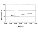
- SiO 2 ratio is a graph showing the XPS analysis results of the transparent conductive film formed using 10 wt% of a target.
- SiO 2 ratio is a graph showing the XPS analysis results of the transparent conductive film formed using a 12.5 wt% of a target.
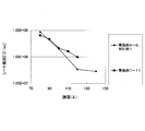
- SiO 2 ratio is a graph showing the XPS analysis results of the transparent conductive film formed using 15 wt%. It is a graph which shows the relationship between a film thickness and sheet resistance. It is a graph which shows the relationship between a film thickness and the transmittance
- SiO 2 ratio in the target is a graph showing the results of a heat resistance test of the transparent conductive film formed. It is a graph which shows the result of the heat resistance test at the time of changing a film thickness. It is a graph which shows the result of a moisture resistance test at the time of changing a film thickness.
- oxygen is added by a known DC magnetron sputtering using a target containing indium tin oxide (ITO) as a main material and containing 10 to 15 wt% silicon oxide. Argon gas was introduced, and a sheet resistance of 10 7 to 10 9 ⁇ / sq. A transparent conductive film as a base is formed.
- ITO indium tin oxide
- a DC magnetron sputtering apparatus For film formation, a DC magnetron sputtering apparatus is used, and a target containing indium tin oxide and 10 to 15% silicon oxide is attached to the cathode for the non-magnetic target, and a glass substrate is placed parallel to and facing the target. Then, a sputtering gas to which oxygen is added is introduced, and film formation is performed under predetermined conditions.
- target-substrate distance 50 to 150 mm
- ultimate vacuum 5 to 8 ⁇ 10 ⁇ 4 Pa
- introduced gas 0.5 to 5.0% (depending on sputtering pressure)
- Ar gas containing oxygen sputtering pressure : 0.1 to 0.5 Pa
- input power DC 1 to 3 W / cm 2
- substrate heating temperature room temperature (no heating) to 70 ° C.
- the transparent conductive film obtained by the method for manufacturing a substrate with a transparent conductive film of the present embodiment is formed on a glass substrate, and is composed of indium tin oxide (ITO) as a main material, and is 7.2 to 11.2 at%.
- ITO indium tin oxide
- the specific resistance is in the order of 10 0 to 10 3 ⁇ ⁇ cm, and the transmittance at a wavelength of 550 nm is 98% or more.
- the film thickness is in the range of 90 to 130 mm, and the sheet resistance is 10 7 to 10 9 ⁇ / sq. A stand is preferable.
- the substrate with a transparent conductive film of the present embodiment includes a glass substrate and the transparent conductive film of the present embodiment formed on the glass substrate.
- IPS liquid crystal cell and capacitive touch panel Moreover, the IPS liquid crystal cell C of FIG. 1 provided with the substrate with a transparent conductive film of this embodiment and the in-cell capacitive touch panel provided with the IPS liquid crystal cell C can be produced.
- IPS In-Plane-Switching
- the liquid crystal is rotated in the substrate plane by a horizontal electric field applied between a pair of comb electrodes provided on one substrate. It is a method to perform.
- a liquid crystal cell is one in which spacers are dispersed between a TFT substrate and a color filter substrate, precisely aligned, injected with liquid crystal, cut into each panel size, and a film such as a polarizing plate adhered.
- FIG. 1 shows a cross section.
- the in-cell type is a system in which a touch panel function is incorporated in a liquid crystal cell in a panel in which a liquid crystal panel and a touch panel are integrated.
- the electrostatic capacitance type is a form in which a position is detected by detecting a change in electrostatic capacitance between a fingertip and a detection electrode formed by patterning a conductive film.
- the liquid crystal cell C of the present embodiment is formed by bonding a color filter substrate 10 and a TFT substrate 20 in a state where the liquid crystal 1 is sealed.
- the color filter substrate 10 is formed by laminating a color filter 13 arranged in a black matrix 12 on the surface of the glass substrate 11 on the liquid crystal 1 side, which is the non-viewing side, and further forming an alignment film 15 thereon. Yes.
- the surface of the color filter substrate 10 opposite to the liquid crystal 1 is provided with the transparent conductive film 3 of the present embodiment, and a cover 8 is laminated thereon via a known polarizing plate 17 and an adhesive layer 7. ing.
- the cover 8 constitutes the surface of the capacitive touch panel and serves as a surface touched by the user.
- the TFT substrate 20 has a pixel electrode 24 made of a comb-shaped transparent electrode formed on the surface of the glass substrate 21 on the liquid crystal 1 side.
- An alignment film 25 is further formed on the surface of the TFT substrate 20 and the pixel electrode 24 on the liquid crystal 1 side, and a polarizing plate is provided on the surface of the TFT substrate 20 on the opposite side of the liquid crystal 1 that is the backlight side via an adhesive layer 37. 27 are stacked.
- the liquid crystal 1 is disposed on the color filter substrate 10 side, and the drive region 4, the sensing region 5, and the ground region 6 are disposed on the TFT substrate 20 side.
- the drive region 4 and the sensing region 5 are obtained by grouping a plurality of common electrodes of display pixels into the drive region 4 and the sensing region 5.
- the common electrode in the drive region 4 is driven by an induction signal from a driver logic (not shown) being transmitted through a drive line.
- a sensing signal sensed by the common electrode in the sensing area 5 is transmitted through a sensing line and processed by an event detection and demodulation circuit in a touch control device (not shown).
- the capacitive touch panel includes a drive circuit board (not shown), electrode terminals, and a light source.
- the glass substrate 11 corresponds to the glass substrate of the present embodiment
- the glass substrate 11 and the transparent conductive film 3 correspond to the substrate with the transparent conductive film of the present embodiment.
- Example 1 Using a target composed of indium tin oxide and 10% (Example 1), 12.5% (Example 2), and 15% (Example 3) of silicon dioxide, the target was formed by DC magnetron sputtering under the following conditions. Filmed.
- Sputtering equipment Carousel type batch type sputtering equipment Target: Square type, thickness 6mm
- Sputtering method DC magnetron sputtering
- Exhaust device Turbo molecular pump Ultimate vacuum: 5 ⁇ 10 ⁇ 4 Pa Ar flow rate: 450 sccm
- Substrate temperature 70 ° C
- Sputtering power 1.55 W / cm 2
- Table 1 shows the ratio (wt%) of silicon oxide contained in the target, the sheet resistance, specific resistance, transmittance, film thickness, and composition ratio of each element in the film (at%) of the formed transparent conductive film. ).
- the formed transparent conductive film has a specific resistance of about 10 0 to 10 3 ⁇ ⁇ cm and a sheet resistance of 10 5 to 10 9 ⁇ / sq at a film thickness of 125 to 127 mm. . It was found that the specific resistance and sheet resistance were very high even when compared with a conventional transparent conductive film, and an unprecedented high resistance transparent conductive film was obtained. Further, from Table 1 and FIGS. 3 and 5, the transparent conductive film formed has a transmittance of 98 to 99% at 550 nm. From Table 1 and FIGS. It was found that a highly transmissive transparent conductive film was obtained.
- the state of silicon contained in the transparent conductive films of Examples 1 to 3 was analyzed by XPS (X-ray Photoelectron Spectroscopy) high-resolution measurement. The measurement results are shown in FIGS. 6 to 8, the intensity peak appears near the binding energy of 102 eV. It is known that the Si peak is around 99 eV, the SiO 2 peak is around 103 eV, the SiO x N y peak is around 102 eV, and the Si 3 N 4 peak is around 101 eV (source: SCAS Technical News XPS). In this embodiment, since the target is made of indium tin oxide and silicon dioxide, and the introduced gas is oxygen, the silicon contained in the transparent conductive films of Examples 1 to 3 is an oxide. It was determined that
- the film thickness is 80, 100, 120, and 140 mm (Examples 4 to 6, proportional 1), and when the oxygen flow rate is 6.6 sccm, 80, 90, 100, and 110 , 120 mm (Examples 7 to 11).
- the ratio of introduced oxygen in the sputtering gas of Examples 4 to 6 and Comparative Example 1 was 1.6%, and the ratio of introduced oxygen in the sputtering gas of Examples 7 to 11 was 4.2%.
- the contrast 1 is a contrast outside the scope of the present invention because the transmittance is less than 98%.
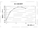
- FIG. 9 and FIG. 10 show the film thickness, sheet resistance, specific resistance, and transmittance of the formed transparent conductive film in Examples 4 to 6, Comparative Example 1, and Examples 7 to 11. Showing the relationship.
- the formed transparent conductive film has a specific resistance of about 10 1 to 10 2 ⁇ ⁇ cm at a film thickness of 80 to 120 mm, and the transmittance at 550 nm is almost all. It was found that an unprecedented high resistance and high transmittance transparent conductive film was obtained.
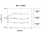
- Test Example 3 The glass substrate with a transparent conductive film on which the transparent conductive film of Examples 1 to 3 was formed in Test Example 1 was held at 120 ° C. in the atmosphere for 0 hour, 1 hour, 2 hours, 3 hours, and after each hold The sample was subjected to a heat resistance test for measuring sheet resistance. The measurement results are shown in FIG. As a result of the heat resistance test, in all of Examples 1 to 3, the sheet resistance hardly changed after being held at 120 ° C. in the atmosphere for 0 hour, 1 hour, 2 hours, 3 hours, up to 3 hours at 120 ° C. It was found that the film had high heat resistance.
- Test Example 4 The glass substrate with a transparent conductive film on which the transparent conductive film of Examples 4 to 6 was formed in Test Example 2 was held at 120 ° C. in the atmosphere for 0 hour, 1 hour, 2 hours, 3 hours, and after each hold The sample was subjected to a heat resistance test for measuring sheet resistance. The measurement results are shown in FIG. As a result of the heat resistance test, all of Examples 4 to 6 were maintained at 120 ° C. in the atmosphere for 0 hours, 1 hour, 2 hours, and 3 hours, and then the sheet resistance did not change greatly, and the temperature was 120 ° C. for 3 hours It was found that the film had high heat resistance.
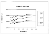
- Test Example 5 The glass substrate with a transparent conductive film on which the transparent conductive film of Examples 4 to 6 was formed in Test Example 2 was placed in a constant temperature and humidity chamber set at a temperature of 60 ° C. and a humidity of 90%, at 0, 90, 150, 198, 246. , 342, 582, 750, and 1014 hours, and each sample after being held was subjected to a moisture resistance test for measuring sheet resistance.
- the measurement results are shown in FIG.
- the sheet resistance did not change greatly after being held at 60 ° C. and 90% for 0 to 1014 hours, and the conditions of 60 ° C. and 90% for 0 to 1014 hours were maintained.
- the rate of change tends to be large when the film thickness is thin, it was found to have high moisture resistance.
- the proportions of introduced oxygen in the sputtering gas of Comparative 2, 3, Examples 12-14, and Comparative 4 are 0%, 0.4%, 0.9%, 1.3%, and 1.8%, respectively. 2.2%.
- the film thickness was in the range of 117 to 126 mm.
- FIG. 14 and FIG. 15 show the relationship between the oxygen introduction amount and the sheet resistance, specific resistance and transmittance.
- the formed transparent conductive film obtained a transmittance of 98% or more, except for the proportions 2 and 3 with an oxygen flow rate of 2 sccm or less.
- the specific resistance when the oxygen flow rate is 10 sccm, the proportionality 4 exceeds the predetermined range of 10 4 ⁇ ⁇ cm, and considering both, the oxygen flow rate is 4 to 8 sccm (oxygen concentration in the sputtering gas: 0.88 to 1). .75%) was found to be suitable. Within this range, changes in sheet resistance and specific resistance are small, which is advantageous from the viewpoint of control during film formation.
- Liquid crystal cell 1 Liquid crystal 2 Spacer 3 Transparent conductive film 4 Drive area 5 Sensing area 6 Ground area 7, 37 Adhesive layer 8 Cover 10 Color filter substrate 11, 21 Glass substrate 12 Black matrix 13 Color filter 15, 25 Alignment films 17, 27 Polarizing plate 20 TFT substrate 24 Pixel electrode (transparent electrode)
Landscapes
- Engineering & Computer Science (AREA)
- Chemical & Material Sciences (AREA)
- Theoretical Computer Science (AREA)
- General Engineering & Computer Science (AREA)
- Physics & Mathematics (AREA)
- General Physics & Mathematics (AREA)
- Human Computer Interaction (AREA)
- Chemical Kinetics & Catalysis (AREA)
- Materials Engineering (AREA)
- Mechanical Engineering (AREA)
- Metallurgy (AREA)
- Organic Chemistry (AREA)
- Physical Vapour Deposition (AREA)
- Non-Insulated Conductors (AREA)
- Manufacturing Of Electric Cables (AREA)
Applications Claiming Priority (2)
| Application Number | Priority Date | Filing Date | Title |
|---|---|---|---|
| JP2012004403A JP5855948B2 (ja) | 2012-01-12 | 2012-01-12 | 透明導電膜,透明導電膜付き基板,ips液晶セル,静電容量型タッチパネル及び透明導電膜付き基板の製造方法 |
| JP2012-004403 | 2012-01-12 |
Publications (1)
| Publication Number | Publication Date |
|---|---|
| WO2013105654A1 true WO2013105654A1 (fr) | 2013-07-18 |
Family
ID=48781595
Family Applications (1)
| Application Number | Title | Priority Date | Filing Date |
|---|---|---|---|
| PCT/JP2013/050439 Ceased WO2013105654A1 (fr) | 2012-01-12 | 2013-01-11 | Film électroconducteur transparent, substrat ayant un film électroconducteur transparent fixé à sa surface, cellule ips à cristaux liquides, écran tactile capacitif, et procédé de fabrication de substrat ayant un film électroconducteur transparent fixé à sa surface |
Country Status (3)
| Country | Link |
|---|---|
| JP (1) | JP5855948B2 (fr) |
| TW (1) | TWI552169B (fr) |
| WO (1) | WO2013105654A1 (fr) |
Cited By (1)
| Publication number | Priority date | Publication date | Assignee | Title |
|---|---|---|---|---|
| CN113981372A (zh) * | 2021-10-26 | 2022-01-28 | 京东方科技集团股份有限公司 | 高阻膜及其制作方法、触控显示面板、显示装置 |
Families Citing this family (18)
| Publication number | Priority date | Publication date | Assignee | Title |
|---|---|---|---|---|
| JP6553950B2 (ja) * | 2015-05-27 | 2019-07-31 | 日東電工株式会社 | 透明導電性フィルムおよびその製造方法 |
| CN106249930A (zh) * | 2015-06-05 | 2016-12-21 | 群创光电股份有限公司 | 触控显示面板及使用其的触控显示设备 |
| JP6779672B2 (ja) * | 2016-06-20 | 2020-11-04 | 株式会社アルバック | 透明導電膜付き基板、液晶パネル及び透明導電膜付き基板の製造方法 |
| WO2018029886A1 (fr) * | 2016-08-10 | 2018-02-15 | 株式会社アルバック | Substrat à couche conductrice transparente, panneau à cristaux liquides et procédé de production de substrat à couche conductrice transparente |
| JP6842927B2 (ja) | 2017-01-06 | 2021-03-17 | 株式会社ジャパンディスプレイ | タッチ検出装置及びタッチ検出機能付き表示装置 |
| JP6849481B2 (ja) | 2017-03-02 | 2021-03-24 | 株式会社ジャパンディスプレイ | 検出装置及び表示装置 |
| WO2018211792A1 (fr) * | 2017-05-15 | 2018-11-22 | 三井金属鉱業株式会社 | Cible de pulvérisation pour film conducteur transparent |
| WO2018211793A1 (fr) * | 2017-05-15 | 2018-11-22 | 三井金属鉱業株式会社 | Cible de pulvérisation cathodique pour film conducteur transparent |
| JP7378952B2 (ja) * | 2018-04-25 | 2023-11-14 | ナガセケムテックス株式会社 | 透明導電膜を有する光学積層体、及びコーティング組成物 |
| WO2019208240A1 (fr) * | 2018-04-26 | 2019-10-31 | 三菱マテリアル株式会社 | Couche de protection, procédé de production de couche de protection, et cible de pulvérisation d'oxyde |
| JP6705526B2 (ja) | 2018-04-26 | 2020-06-03 | 三菱マテリアル株式会社 | シールド層、シールド層の製造方法、及び、酸化物スパッタリングターゲット |
| JP2020033639A (ja) | 2018-08-27 | 2020-03-05 | 三菱マテリアル株式会社 | 酸化物スパッタリングターゲット、及び、酸化物スパッタリングターゲットの製造方法 |
| KR102102548B1 (ko) | 2018-12-11 | 2020-04-21 | 주식회사 네이션스 | 투명 전기 차폐층을 구비한 기판, 및 투명 전기 차폐층을 구비한 터치 스크린 디스플레이 |
| JP7256647B2 (ja) * | 2019-01-29 | 2023-04-12 | 株式会社ジャパンディスプレイ | 表示装置 |
| JP2020204050A (ja) * | 2019-06-14 | 2020-12-24 | 株式会社アルバック | 透明導電膜の製造方法、透明導電膜、及びスパッタリングターゲット |
| KR102726987B1 (ko) | 2019-11-11 | 2024-11-05 | 엘지디스플레이 주식회사 | 액정표시장치 |
| JP2021088730A (ja) | 2019-12-02 | 2021-06-10 | 三菱マテリアル株式会社 | 酸化物スパッタリングターゲット、及び、酸化物スパッタリングターゲットの製造方法 |
| JP2024021364A (ja) | 2022-08-03 | 2024-02-16 | シャープディスプレイテクノロジー株式会社 | インセルタッチパネル |
Citations (5)
| Publication number | Priority date | Publication date | Assignee | Title |
|---|---|---|---|---|
| JPS6389656A (ja) * | 1986-10-01 | 1988-04-20 | Agency Of Ind Science & Technol | 透明導電膜及びその生成方法 |
| JPH04206403A (ja) * | 1990-11-30 | 1992-07-28 | Nitto Denko Corp | アナログ式タツチパネル |
| JP2003105532A (ja) * | 2001-06-26 | 2003-04-09 | Mitsui Mining & Smelting Co Ltd | 高抵抗透明導電膜用スパッタリングターゲット及び高抵抗透明導電膜の製造方法 |
| JP2003277921A (ja) * | 2002-03-19 | 2003-10-02 | Nikko Materials Co Ltd | 高抵抗透明導電性膜用スパッタリングターゲット |
| JP2007138266A (ja) * | 2005-11-21 | 2007-06-07 | Mitsui Mining & Smelting Co Ltd | 高抵抗透明導電膜用スパッタリングターゲット及び高抵抗透明導電膜並びにその製造方法 |
Family Cites Families (6)
| Publication number | Priority date | Publication date | Assignee | Title |
|---|---|---|---|---|
| TW256931B (fr) * | 1993-02-24 | 1995-09-11 | Sumitomo Metal Mining Co | |
| JPH07196365A (ja) * | 1993-12-28 | 1995-08-01 | Showa Denko Kk | Ito焼結体ならびにito透明電導膜およびその膜の形成方法 |
| TW446637B (en) * | 1996-05-28 | 2001-07-21 | Mitsui Chemicals Inc | Transparent laminates and optical filters for displays using the same |
| JP2001307553A (ja) * | 2000-04-24 | 2001-11-02 | Geomatec Co Ltd | 透明導電膜およびその製造方法並びにその用途 |
| US6908574B2 (en) * | 2001-08-13 | 2005-06-21 | Dowa Mining Co., Ltd. | Tin-containing indium oxides, a process for producing them, a coating solution using them and electrically conductive coatings formed of them |
| KR20100067119A (ko) * | 2007-10-03 | 2010-06-18 | 미츠이 긴조쿠 고교 가부시키가이샤 | 산화인듐계 투명 도전막 및 그 제조방법 |
-
2012
- 2012-01-12 JP JP2012004403A patent/JP5855948B2/ja active Active
-
2013
- 2013-01-11 TW TW102101092A patent/TWI552169B/zh active
- 2013-01-11 WO PCT/JP2013/050439 patent/WO2013105654A1/fr not_active Ceased
Patent Citations (5)
| Publication number | Priority date | Publication date | Assignee | Title |
|---|---|---|---|---|
| JPS6389656A (ja) * | 1986-10-01 | 1988-04-20 | Agency Of Ind Science & Technol | 透明導電膜及びその生成方法 |
| JPH04206403A (ja) * | 1990-11-30 | 1992-07-28 | Nitto Denko Corp | アナログ式タツチパネル |
| JP2003105532A (ja) * | 2001-06-26 | 2003-04-09 | Mitsui Mining & Smelting Co Ltd | 高抵抗透明導電膜用スパッタリングターゲット及び高抵抗透明導電膜の製造方法 |
| JP2003277921A (ja) * | 2002-03-19 | 2003-10-02 | Nikko Materials Co Ltd | 高抵抗透明導電性膜用スパッタリングターゲット |
| JP2007138266A (ja) * | 2005-11-21 | 2007-06-07 | Mitsui Mining & Smelting Co Ltd | 高抵抗透明導電膜用スパッタリングターゲット及び高抵抗透明導電膜並びにその製造方法 |
Cited By (1)
| Publication number | Priority date | Publication date | Assignee | Title |
|---|---|---|---|---|
| CN113981372A (zh) * | 2021-10-26 | 2022-01-28 | 京东方科技集团股份有限公司 | 高阻膜及其制作方法、触控显示面板、显示装置 |
Also Published As
| Publication number | Publication date |
|---|---|
| TWI552169B (zh) | 2016-10-01 |
| JP5855948B2 (ja) | 2016-02-09 |
| TW201333985A (zh) | 2013-08-16 |
| JP2013142194A (ja) | 2013-07-22 |
Similar Documents
| Publication | Publication Date | Title |
|---|---|---|
| JP5855948B2 (ja) | 透明導電膜,透明導電膜付き基板,ips液晶セル,静電容量型タッチパネル及び透明導電膜付き基板の製造方法 | |
| TWI233570B (en) | Touch panel display apparatus and method of fabricating the same | |
| JP5375536B2 (ja) | 静電容量式タッチパネルとその製造方法及び該タッチパネルを備えた液晶表示装置 | |
| US20150062710A1 (en) | Transparent body for use in a touch panel and its manufacturing method for apparatus | |
| CN105264468A (zh) | 压力检测显示装置和电子设备 | |
| EP3285152B1 (fr) | Dispositif d'affichage à commande tactile ayant une couche à haute résistance | |
| KR102042081B1 (ko) | 투명 도전층이 구비된 기판, 액정 패널 및 투명 도전층이 구비된 기판의 제조 방법 | |
| CN111902561A (zh) | 屏蔽层、屏蔽层的制造方法及氧化物溅射靶 | |
| CN104145239A (zh) | 输入装置 | |
| 금민종 et al. | Preparation of ITO thin film by using DC magnetron sputtering | |
| CN203870356U (zh) | 一种On-cell技术中触控层的防静电结构 | |
| JP6779672B2 (ja) | 透明導電膜付き基板、液晶パネル及び透明導電膜付き基板の製造方法 | |
| JP2000113732A (ja) | 透明導電膜とその製造方法、透明導電膜付き基板およびタッチパネル | |
| KR101755694B1 (ko) | 터치 패널, 이의 제조 방법 및 터치 패널을 포함한 액정 표시 장치 | |
| KR102102548B1 (ko) | 투명 전기 차폐층을 구비한 기판, 및 투명 전기 차폐층을 구비한 터치 스크린 디스플레이 | |
| CN107167954A (zh) | 一种具备触控感应功能彩色滤光片及其制造方法 | |
| US20190064569A1 (en) | Antistatic film and display input device | |
| KR101955005B1 (ko) | 터치 스크린 패널에서 사용하기 위한 층 시스템, 터치 스크린 패널에서 사용하기 위한 층 시스템을 제조하기 위한 방법, 및 터치 스크린 패널 | |
| JP2015003493A (ja) | 透明導電膜付構造体および素子、電子機器 | |
| TW201312205A (zh) | 觸摸屏面板 | |
| CN2852184Y (zh) | 平面显示装置 | |
| KR101492215B1 (ko) | RF/DC 동시인가 마그네트론 스퍼터링법을 이용한 ITO:Ce 초박막, 이의 제조방법 및 이를 포함하는 터치 패널 | |
| JP2007188707A (ja) | 透明導電膜及びその製造方法、並びにタッチパネル | |
| JP2013175240A (ja) | 静電容量式タッチパネル及び該タッチパネルを備えた液晶表示装置 |
Legal Events
| Date | Code | Title | Description |
|---|---|---|---|
| 121 | Ep: the epo has been informed by wipo that ep was designated in this application |
Ref document number: 13736227 Country of ref document: EP Kind code of ref document: A1 |
|
| NENP | Non-entry into the national phase |
Ref country code: DE |
|
| 122 | Ep: pct application non-entry in european phase |
Ref document number: 13736227 Country of ref document: EP Kind code of ref document: A1 |