WO2013114469A1 - Dispositif terminal portable - Google Patents
Dispositif terminal portable Download PDFInfo
- Publication number
- WO2013114469A1 WO2013114469A1 PCT/JP2012/001688 JP2012001688W WO2013114469A1 WO 2013114469 A1 WO2013114469 A1 WO 2013114469A1 JP 2012001688 W JP2012001688 W JP 2012001688W WO 2013114469 A1 WO2013114469 A1 WO 2013114469A1
- Authority
- WO
- WIPO (PCT)
- Prior art keywords
- spacer
- connection spring
- terminal device
- housing
- opening
- Prior art date
- Legal status (The legal status is an assumption and is not a legal conclusion. Google has not performed a legal analysis and makes no representation as to the accuracy of the status listed.)
- Ceased
Links
Images







Classifications
-
- H—ELECTRICITY
- H04—ELECTRIC COMMUNICATION TECHNIQUE
- H04M—TELEPHONIC COMMUNICATION
- H04M1/00—Substation equipment, e.g. for use by subscribers
- H04M1/02—Constructional features of telephone sets
- H04M1/0202—Portable telephone sets, e.g. cordless phones, mobile phones or bar type handsets
- H04M1/0249—Details of the mechanical connection between the housing parts or relating to the method of assembly
Definitions
- the present invention relates to a portable terminal device in which a plurality of parts are accommodated in a casing.
- the casing of the portable terminal device there may be adopted a case in which an opening for inserting a part is formed on one side and a frame edge for fixing a lid or a display panel is formed around the opening.
- a concave space (see the space UC in FIG. 3) that is wider than the opening is formed on the back side of the frame edge. This space is formed by an undercut process during resin molding. Below, this concave space part is also called an undercut part.
- the arrangement of the components mounted in the housing is determined in consideration of various factors. For example, components used for exchanging information with the outside, such as a light emitting element or a touch sensor, are determined in consideration of visibility or operability. In addition, there are parts such as an antenna whose arrangement is determined so that good characteristics can be obtained. In addition, the arrangement of components may be determined in consideration of the workability of the assembly process, such as making it possible to temporarily fix the components during the assembly process of the apparatus.
- Patent Document 1 As a related art related to the present invention, in Patent Document 1, two frames having elastic protrusions are provided on the back side of the front casing of the apparatus, and a display panel is fitted to the elastic protrusions of the two frames. A structure to be fixed is disclosed.
- the parts When the parts are packed and placed in the space of the undercut part of the housing, the parts are integrated and the diameter of the parts is larger than the opening diameter of the housing, and the size is adjusted to the wide diameter inside the housing. If this is the case, this part cannot be put into the casing without any ingenuity.
- Patent Document 1 when the components disclosed in Patent Document 1 are applied and components are arranged in the casing, there arises a problem that the rigidity of the casing becomes low or the molding of the casing becomes difficult.
- the narrowed frame edge portion of the opening of the housing is formed of an elastic body, and the frame edge portion is widened to push the component.
- the part can be inserted from the opening of the housing into the interior, and then the part can be slid into the space of the undercut portion.
- an unnecessary empty space is generated in the housing as the components are slid. If an unnecessary empty space is generated in the housing, the rigidity of the apparatus is reduced accordingly.
- an unnecessary empty space is generated in the housing, there arises a problem that an extra fixing structure is required to prevent the parts from wobbling in this space.
- a portable terminal device includes a housing having an opening on one side and a housing space having a larger diameter than the diameter of the opening, a first component housed in the housing space, A second part housed in the housing space in parallel with the first part; and a spacer interposed between the first part and the second part, wherein the spacer comprises the first part and the first part.
- one or both of the first component and the second component can be easily packed and arranged in the space of the undercut portion of the casing. Unnecessary empty space is not generated for the arrangement.
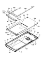
- FIG. 1 is an exploded perspective view showing the entirety of a mobile terminal device according to a first embodiment of the present invention.
- FIG. 3 is an exploded perspective view in which the periphery of the electronic component according to the first embodiment is separated.
- a longitudinal sectional view showing the periphery of the frame edge of the housing The perspective view which shows the holding member of an electronic component Perspective view showing spacer Perspective view of spacer viewed from back side
- a longitudinal sectional view showing a state in which a sheet metal member and an electronic component are inserted into the housing Longitudinal sectional view showing the state in the middle of inserting the spacer Longitudinal sectional view showing the periphery of the spacer and electronic components in the assembled state
- the disassembled perspective view which shows the whole portable terminal device of Embodiment 2.
- FIG. 2 is an exploded perspective view showing the entirety of a mobile terminal device according to a first embodiment of the present invention.
- FIG. 3 is an exploded perspective view in which the periphery of the electronic component according
- the exploded perspective view which looked at the spacer of Embodiment 2 with the electronic component side facing forward The exploded perspective view which looked at the spacer of Embodiment 2 with the sheet metal member side facing forward
- the disassembled perspective view of the state which combined the spacer main body and shield member of Embodiment 2 A longitudinal sectional view showing the periphery of the spacer of the mobile terminal device of the second embodiment
- FIG. 1 is an exploded perspective view showing the entire portable terminal device according to the first embodiment of the present invention
- FIG. 2 is an exploded perspective view in which the periphery of an electronic component is separated.
- the mobile terminal device is a multi-function mobile phone called a so-called smartphone.
- the portable terminal device includes a display panel 10, a sheet metal member 20, an electronic component 30, a housing 50, and a spacer 60.
- An electronic substrate 40 and a battery pack are held on the back side of the sheet metal member 20 (downward in FIG. 1).
- the sheet metal member 20 corresponds to a first component
- the electronic component 30 corresponds to a second component.
- the housing 50 is of a so-called bathtub type having a shallow accommodation space that is open on one wide surface and is surrounded by a bottom surface and a side wall (corresponding to a side wall portion) 52 with the opening being upward.
- the bottom surface side and the lateral side of the housing 50 are almost entirely covered except for holes used for predetermined functions of the apparatus, such as a camera lens hole 56 and a connector insertion hole 57.
- the casing 50 is integrally formed by resin injection molding.
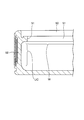
- FIG. 3 is a longitudinal sectional view showing the periphery of the frame edge of the housing.
- a frame edge (corresponding to a protruding portion) 51 is formed around the opening of the housing 50 so as to protrude from the side wall 52 to the inside of the opening.
- the frame edge 51 is a part to which the edge part of the display panel 10 is bonded and fixed.
- the back side of the frame edge 51 is an undercut portion, and a space UC (FIG. 3) wider than the opening W is formed.
- FIGS. 1 and 2 a plurality of engaging grooves 53 for locking the engaging portion 23 of the sheet metal member 20 are formed on the side wall 52 of the housing 50. Also, screw holes (screws S are stopped in FIGS. 1 and 2) for fixing the sheet metal member 20 are provided at the four corners of the housing 50.
- FIG. 4 is a perspective view showing a holding member for the electronic component.
- the electronic component 30 includes the holding member 31 in FIG. 4, a metallic antenna member provided in the holding member 31, a first flexible substrate 33, and a second flexible substrate 34.
- the holding member 31 is a long block-shaped member on one side, and is formed with a storage portion for storing the antenna member on the metal plate bent in a complicated manner. Further, on the surface of the holding member 31 facing the spacer 60, a positioning groove 31a into which the convex portion of the spacer 60 is fitted is formed.
- a plurality of light-emitting elements E are mounted on the surface of the first flexible substrate 33 on the display panel 10 side, and are connected to the electronic substrate 40 via a flexible cable 33a.
- the first flexible substrate 33 includes an upper surface (a surface on the display panel 10 side), a lower surface (a surface on the bottom surface side of the housing 50), and one side surface (a surface entering the undercut portion of the housing 50) of the holding member 31. ) And is held on the upper and lower surfaces of the holding member 31 (see FIGS. 7 to 9). An intermediate portion 33 b along one side surface of the holding member 31 in the first flexible substrate 33 is slightly separated from the holding member 31 to exert a spring action.
- a plurality of proximity sensors N are mounted on the second flexible substrate 34, and a cushion sheet 34b (see FIGS. 7 to 9) is provided on the back side.
- the second flexible substrate 34 is connected to the electronic substrate 40 via a flexible cable 34a.
- the second flexible board 34 is not locked to the holding member 31 and the first flexible board 33, and is stacked on the first flexible board 33 with the top plate portion 65 of the spacer 60 interposed therebetween.
- the sheet metal member 20 is configured by pressing and bending a metal plate and further forming a resin partly by insert molding.
- the sheet metal member 20 has a substantially rectangular shape extending in the direction along the opening of the housing 50, and the surrounding portions are upright portions 22a and 22b (see FIG. 2) that are bent substantially at right angles to the plate surface in order to increase rigidity. Reference) is formed.
- the raised portions 22b formed on the side facing the spacer 60 are formed with engaged portions (for example, engagement holes) 22c and 22c with which engagement claws 61b and 61b of the spacer 60 described later are engaged. Has been.
- a plurality of engaging portions 23 that are engaged with the engaging grooves 53 of the housing 50 are formed of resin. Further, through holes 25 for being screwed to the housing 50 are formed at the four corners of the sheet metal member 20.
- FIG. 5 is a perspective view showing the spacer
- FIG. 6 is a perspective view of the spacer viewed from the back side.
- the spacer 60 has a wedge-shaped wedge part 61 inserted between the electronic component 30 and the sheet metal member 20, and a top plate part 65 projecting laterally from the upper end of the wedge part 61, and is made of an elastic resin. It is configured.
- the wedge part 61 is formed with a convex part 61 a that fits into the concave groove 31 a of the holding member 31 of the electronic component 30.
- the wedge portion 61 is formed with engaging claws (corresponding to an engaging portion) 61 b and 61 b that engage with the engaged portions 22 c and 22 c of the standing portion 22 b of the sheet metal member 20.
- the top plate portion 65 is configured to cover the upper part (the display panel 10 side) of the electronic component 30, and a light guide hole 65 a that guides light is formed in a portion overlapping the light emitting element E of the first flexible substrate 33. Yes.
- a light guide hole 34h (see FIGS. 7 to 9) for guiding light to a portion overlapping the light emitting element E is also formed in the cushion sheet 34b on the lower side of the second flexible substrate 34.
- FIG. 7 is a longitudinal sectional view showing a state in which the sheet metal member and the electronic component are inserted into the housing
- FIG. 8 is a longitudinal sectional view showing a state in the middle of inserting the spacer
- FIG. 9 is a state in which the apparatus is assembled. It is a longitudinal cross-sectional view which shows the periphery of a spacer and an electronic component.
- the sheet metal member 20 and the electronic component 30 are connected through the opening W (see FIG. 3) of the housing 50. Put in the containment space. At this time, the other end side (the opposite end of the electronic component 30) of the sheet metal member 20 is first inserted into the space of the undercut portion of the housing 50, and the sheet metal member 20 rotates and moves with this portion as a fulcrum. Thus, the end portion on the electronic component 30 side is placed in the housing 50. In this state, the engagement portion 23 of the sheet metal member 20 is engaged with the engagement groove 53 of the housing 50, and the sheet metal member 20 is fixed to the housing 50.
- the second flexible substrate 34 is floated and the spacer 60 is pushed between the sheet metal member 20 and the electronic component 30.
- the wedge portion 61 of the spacer 60 spreads between the sheet metal member 20 and the electronic component 30, and the electronic component 30 is pushed and packed into the space of the undercut portion of the housing 50 by this action.
- the convex part 61a of the wedge part 61 advances along the concave groove 31a of the holding member 31, and the wedge part 61 is pushed to the end, whereby the engagement claws 61b and 61b (see FIG. 5) of the wedge part 61 are formed.
- the sheet metal member 20 is engaged with the engaged portions 22c and 22c (see FIG. 2) of the upright portion 22b. By engaging these, the spacer 60 and the electronic component 30 are fixed.
- the intermediate portion 33b of the first flexible substrate 33 of the electronic component 30 hits the side wall 52 of the housing 50 and generates stress by the action of a spring.
- the wedge part 61 is not comparatively large, since it has elasticity, the stress toward the electronic component 30 side also arises in the wedge part 61. Due to these stresses, the spacer 60 and the electronic component 30 are securely fixed, and subsequent occurrence of backlash is eliminated.
- the screws S are fixed to the housing 50 through the through holes 25 at the four corners of the sheet metal member 20 and the through holes 33 d and 33 d at both ends of the first flexible substrate 33.
- the screwing of the first flexible substrate 33 is for surely connecting the ground to the sheet metal member 20 and is not intended for fixing.
- the edge of the entire periphery of the display panel 10 is bonded to the frame edge 51 of the housing 50 with an adhesive.
- the second flexible substrate 34 is supported by the top plate portion 65 of the spacer 60 and the cushion sheet 34b, and is fixed in close contact with the display panel 10. Therefore, the proximity sensor N can accurately detect a finger touch operation on the display panel 10.
- the periphery of the light emitting element E of the first flexible substrate 33 is surrounded by the light guide hole 65a of the top plate portion 65 of the spacer 60 and the light guide hole 34h of the cushion sheet 34b. Therefore, the light from the light emitting element E is guided to the display panel 10 and output to the outside, and the light is prevented from leaking to the outside of the light guide holes 65a and 34h.
- the spacer 60 pushes the space between the sheet metal member 20 and the electronic component 30, so that the electronic component 30 can be easily removed from the undercut portion of the housing 50. Can be packed and fixed in the space.
- the internal components are arranged in the casing. 50 can be placed in the space of the undercut portion in 50. Moreover, it is possible to make a state (fixed) where internal components are appropriately temporarily fixed in the housing 50 during the assembly process.
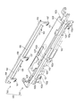
- FIG. 10 is an exploded perspective view showing the entire mobile terminal device according to the second embodiment.
- the portable terminal device of the second embodiment is different from the first embodiment in that a shield member 165 is provided on the spacer 160.
- the same components as those in the first embodiment are denoted by the same reference numerals, and detailed description thereof is omitted.
- the mobile terminal device includes a display panel 110, a sheet metal member 120, an electronic component 130, an electronic substrate 40, a housing 150, and a spacer 160.
- the display panel 110 is, for example, a liquid crystal module, and includes an outer panel 111 (see FIG. 14), a display element layer 114 (see FIG. 14), a backlight layer 115 (see FIG. 14), and the like.
- the central part of the entire area of the outer panel 111 is set in the display area 112.
- the display element layer 114 and the backlight layer 115 are fixed to the same area as the display area 112 on the back side of the outer panel 111.
- a display drive circuit (integrated circuit) 113 is provided at one end side of the display area 112 on the back side of the outer panel 111, and a flexible cable 118 (see FIG. 14) is connected to the display drive circuit 113.
- the electronic component 130 has a configuration in which a metallic antenna member is held by a resin holding member 31.
- the housing 150 has substantially the same configuration as that of the housing 50 of the first embodiment except that the housing 150 has an opening 158 for inserting and removing the battery pack and a battery lid 159 that closes the opening 158.
- the sheet metal member 120 has substantially the same configuration as the sheet metal member 20 of the first embodiment except that the L-shaped sheet metal 29 is mainly not provided.
- an L-shaped sheet metal 29 (see FIGS. 2 and 9) is provided at one end of the sheet metal member 20.
- the L-shaped sheet metal 29 is configured by bending the sheet metal into an L shape, and the bent portion is fixed in a state of protruding from the plate surface of the sheet metal member 20 toward the display panel 10.
- the L-shaped metal plate 29 partitions the display drive circuit 18 (see FIG. 1) of the display panel 10 and the electronic component 30 and shields electromagnetic noise transmitted from the display drive circuit 18 to the antenna member of the electronic component 30. To play a role.
- the L-shaped metal plate 29 is disposed at a position outside the display area 12 of the display panel 10, that is, in a range where the display element layer is not provided on the back side of the display panel 10 and is thin.
- the display region 12 of the display panel 10 is designed to have a size that does not exceed the lower edge of the sheet metal member 20 (side adjacent to the electronic component 30).
- An L-shaped sheet metal 29 can be provided on the lower edge of the member 20.
- the display area 112 of the display panel 110 is designed to have a size exceeding the edge of the lower side (side adjacent to the electronic component 130) of the sheet metal member 120. That is, the display element layer 114 and the backlight layer 115 of the display panel 110 are provided up to a range where they overlap the lower edge of the sheet metal member 120. Therefore, the display panel 110 is thick at this portion, and it is difficult to provide the L-shaped sheet metal 29 at the lower edge of the sheet metal member 120.
- FIG. 11 to 13 show detailed views of the spacer according to the second embodiment.
- 11 and 12 are exploded perspective views in which the spacer main body and the shield member are separated,
- FIG. 11 is a view when the electronic component 130 side is facing forward, and
- FIG. 12 is the sheet metal member 120 side facing forward.
- FIG. 13 is a perspective view of the shield member engaged with the spacer body.
- the spacer 160 includes a spacer body 161 and a shield member 165.
- the shield member 165 is formed by pressing and bending a metal plate.
- the shield member 165 includes a band portion 166 that spreads in the vertical and horizontal directions, a connection spring 167, and locking portions 168 and 169 for fixing to the spacer main body 161.
- the band portion 166 spreads vertically and horizontally between the display drive circuit 113 of the display panel 110 and the electronic component 130 and blocks electromagnetic noise propagation therebetween.
- connection spring 167 is electrically connected to the standing portion 22b of the sheet metal member 120 serving as a frame ground by contacting with a predetermined spring pressure.
- the locking portion 168 is a portion that is locked on the upper side of the spacer body 161 and is provided on the base side of the connection spring 167 in a range that overlaps with the connection spring 167 when viewed in the longitudinal direction of the spacer 160.
- the locking portion 169 is a portion locked on the lower side of the spacer main body 161 and is provided at a position shifted in the longitudinal direction of the connection spring 167 and the spacer 160.
- the spacer body 161 includes a wedge portion 162 inserted between the sheet metal member 120 and the electronic component 130 and a top plate portion 163 projecting horizontally from the upper end of the wedge portion 162, and is integrally formed of resin. ing.
- a notch 162b is formed at a portion where the movable portion of the connection spring 167 is disposed.
- This notch 162b is formed so as to open the back of the movable part of the connection spring 167 (the reverse side of the ground connection side). That is, in the wedge portion 162, there is no configuration for supporting the connection spring 167 behind the movable portion of the connection spring 167.
- the wedge portion 162 is provided with thick portions 162a on both sides of the notch 162b, and the movable portion of the connection spring 167 is disposed between the thick portions 162a.
- the wedge portion 162 and the top plate portion 163 are formed with a locked portion 162f and a locking groove 163f corresponding to the locking portions 168 and 169 of the shield member 165, respectively.
- the locking groove 163f is formed above the notch 162b so as to overlap the notch 162b when viewed in the longitudinal direction of the spacer 160.
- the locking portion 168 of the shield member 165 is hooked and locked in the locking groove 163f.
- the locked portion 162f is formed below the wedge portion 162, and the locking portion 169 of the shield member 165 is hooked and locked.
- the wedge portion 162 and the top plate portion 163 include an engaging claw 162g that engages with the engaged portion 22c of the sheet metal member 20, and an engaging claw 163g that is hooked and locked to the edge of the housing 150. Are formed respectively.
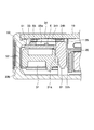
- FIG. 14 is a longitudinal sectional view showing the periphery of the spacer in the mobile terminal device according to the second embodiment.
- the spacer 160 is inserted between the sheet metal member 120 and the electronic component 130. . Thereby, the electronic component 130 is pushed into the space of the undercut portion of the housing 50 and placed.
- the shield member 165 of the spacer 160 is stably connected to the frame ground with the connection spring 167 contacting the upright portion 22b of the sheet metal member 120 with a constant pressure. Therefore, the electromagnetic noise propagating from the display drive circuit 113 to the antenna member of the electronic component 130 can be blocked by the shield member 165, and deterioration of the antenna characteristics can be prevented.
- connection spring support structure Here, the support structure of the connection spring 167 will be described in comparison with the comparative example.
- FIG. 15 is a schematic diagram for explaining the operation of the connection springs (A) and (B) of the comparative example and the connection spring (C) of the second embodiment.
- connection spring 167B As shown in FIG. 15A, a configuration in which a long connection spring 167B is employed and the back of the connection spring 167B is supported by a spacer body 161B will be considered.
- connection spring 167B can be displaced relatively large to generate a large urging force on the connection spring 167B. With this urging force, the connection spring 167B can be stably grounded. Further, since the connection spring 167B bends over a long range, even if the movable end is greatly displaced, the connection spring 167B does not plastically exceed the elastic limit.
- connection spring 167C when the movable end of the connection spring 167C is displaced relatively large to generate a sufficient urging force on the connection spring 167C, the connection spring 167C bends in a short range. May be plastically deformed beyond the elastic limit.
- connection spring 167C cannot be stably grounded.
- connection spring 167 is employed, while a notch 162b is provided behind the connection spring 167 to eliminate support behind the connection spring 167.
- the structure by which the base of the connection spring 167 is latched by the spacer main body 161 is employ adopted.
- connection spring 167 can be displaced greatly by bending over a long range from the vicinity of the root to the movable end. As a result, the connection spring 167 can generate a stable inability to the connection spring 167 without plastic deformation.
- the display element layer 114 and the backlight layer 115 of the display panel 110, the water stop structure 159 b of the battery lid 159, etc. are provided around the spacer 160. Is provided. For this reason, in the configuration of the second embodiment, the arrangement space of the connection spring 167C cannot be secured long in the height direction, and the connection spring 167C cannot be configured long.
- connection spring 167 of the second embodiment can be stably grounded even if a large space around the connection spring 167 cannot be secured in the height direction. it can.
- the height dimension of the spacer 160 can be shortened, and the configuration of the display area 112 of the display panel 110 is less likely to interfere with the configuration of the display unit of the mobile terminal device. It can also contribute to narrowing the frame.
- the spacer 160 pushes the space between the sheet metal member 120 and the electronic component 130, so that the electronic component 130 can be easily removed from the undercut portion of the housing 150. It can be fixed in the space.
- the internal components are arranged in the casing.
- 150 can be arranged in a space in the undercut portion in 150.
- internal components can be placed in the housing 150 during the assembly process.
- electromagnetic noise propagating between one side and the other side of the spacer 160 can be blocked. Therefore, performance degradation due to electromagnetic noise is prevented.
- the configuration in which only one electronic component 30 is moved to the space of the undercut portion of the housing 50 by the spacer 60 has been described as an example.
- the type of component that is packed into the space of the undercut portion of the housing by the spacer is not particularly limited, and various components may be applied.
- the configuration in which the component that generates electromagnetic noise and the component that blocks electromagnetic noise and prevents performance deterioration is used as an example of the display drive circuit and the antenna member has been described. Parts may replace other parts.
- the present invention is useful for mobile terminal devices such as so-called smartphones.
Landscapes
- Engineering & Computer Science (AREA)
- Signal Processing (AREA)
- Telephone Set Structure (AREA)
- Mounting Components In General For Electric Apparatus (AREA)
Abstract
Cette invention concerne un dispositif terminal portable présentant une structure permettant de ranger facilement un élément dans un espace d'une partie creuse d'une enceinte. Ledit dispositif terminal portable comprend : une enceinte (50) présentant une ouverture à une extrémité et un espace de rangement intérieur dont le diamètre est supérieur à celui de l'ouverture ; un premier élément (20) rangé dans l'espace de rangement ; un second élément (31) rangé parallèlement au premier élément dans l'espace de stockage ; et un élément d'espacement (60) interposé ente le premier élément (20) et le second élément (31). Ledit élément d'espacement (60) élargit l'espace entre le premier élément (20) et le second élément (31). Le premier (20) et/ou le second élément (31) est/sont rangé(s) en étant poussé(s) dans la partie de l'espace de rangement présentant un diamètre supérieur à celui de l'ouverture.
Applications Claiming Priority (2)
| Application Number | Priority Date | Filing Date | Title |
|---|---|---|---|
| JP2012019796 | 2012-02-01 | ||
| JP2012-019796 | 2012-02-01 |
Publications (1)
| Publication Number | Publication Date |
|---|---|
| WO2013114469A1 true WO2013114469A1 (fr) | 2013-08-08 |
Family
ID=48904559
Family Applications (1)
| Application Number | Title | Priority Date | Filing Date |
|---|---|---|---|
| PCT/JP2012/001688 Ceased WO2013114469A1 (fr) | 2012-02-01 | 2012-03-12 | Dispositif terminal portable |
Country Status (2)
| Country | Link |
|---|---|
| JP (1) | JPWO2013114469A1 (fr) |
| WO (1) | WO2013114469A1 (fr) |
Cited By (1)
| Publication number | Priority date | Publication date | Assignee | Title |
|---|---|---|---|---|
| JP2016213671A (ja) * | 2015-05-08 | 2016-12-15 | シャープ株式会社 | 携帯機器 |
Citations (2)
| Publication number | Priority date | Publication date | Assignee | Title |
|---|---|---|---|---|
| JPS6418571U (fr) * | 1987-07-22 | 1989-01-30 | ||
| JPH0685473A (ja) * | 1992-08-31 | 1994-03-25 | Murata Mfg Co Ltd | 電子部品及びその製造方法 |
-
2012
- 2012-03-12 JP JP2012527544A patent/JPWO2013114469A1/ja active Pending
- 2012-03-12 WO PCT/JP2012/001688 patent/WO2013114469A1/fr not_active Ceased
Patent Citations (2)
| Publication number | Priority date | Publication date | Assignee | Title |
|---|---|---|---|---|
| JPS6418571U (fr) * | 1987-07-22 | 1989-01-30 | ||
| JPH0685473A (ja) * | 1992-08-31 | 1994-03-25 | Murata Mfg Co Ltd | 電子部品及びその製造方法 |
Cited By (1)
| Publication number | Priority date | Publication date | Assignee | Title |
|---|---|---|---|---|
| JP2016213671A (ja) * | 2015-05-08 | 2016-12-15 | シャープ株式会社 | 携帯機器 |
Also Published As
| Publication number | Publication date |
|---|---|
| JPWO2013114469A1 (ja) | 2015-05-11 |
Similar Documents
| Publication | Publication Date | Title |
|---|---|---|
| KR100724912B1 (ko) | 액정 표시 장치 | |
| KR101702298B1 (ko) | 촬상소자 패키지가 장착된 촬상장치 | |
| JP2014182920A (ja) | トレイタイプカードコネクタ | |
| JP5522732B2 (ja) | 液晶ディスプレイの支持構造及び電子機器 | |
| WO2013114469A1 (fr) | Dispositif terminal portable | |
| JP2006222501A (ja) | 撮像ユニット、撮像装置及び撮像ユニットの製造方法 | |
| JP5439514B2 (ja) | 携帯端末装置 | |
| US8373994B2 (en) | Electronic apparatus including at least two electrically-connectable connectors | |
| JP5654146B2 (ja) | 携帯端末装置 | |
| JP6083317B2 (ja) | シールドケースおよび電子機器 | |
| CN102214967B (zh) | 音圈马达 | |
| US20140118968A1 (en) | Electronic device and electric connector | |
| CN112512228B (zh) | 板状构件的固定结构以及电子设备 | |
| US9013639B2 (en) | Electronic apparatus having a module protection buffer | |
| JP4908659B2 (ja) | 電子機器 | |
| KR20130014948A (ko) | 카메라 모듈 및 그 제조방법 | |
| US8467173B2 (en) | Electronic device and component | |
| CN108020954A (zh) | 背光模块及其应用的显示装置 | |
| JP4751469B2 (ja) | 電子機器 | |
| US20110141703A1 (en) | Mount and electronic device | |
| TWI867296B (zh) | 固定裝置、光學模組及電子設備 | |
| JP5424855B2 (ja) | 電子機器 | |
| JP2012244052A (ja) | 部品固定構造とそれを含む携帯型電子機器 | |
| US20170123464A1 (en) | Electronic device | |
| JP2018169446A (ja) | 電子機器 |
Legal Events
| Date | Code | Title | Description |
|---|---|---|---|
| ENP | Entry into the national phase |
Ref document number: 2012527544 Country of ref document: JP Kind code of ref document: A |
|
| 121 | Ep: the epo has been informed by wipo that ep was designated in this application |
Ref document number: 12867256 Country of ref document: EP Kind code of ref document: A1 |
|
| NENP | Non-entry into the national phase |
Ref country code: DE |
|
| 122 | Ep: pct application non-entry in european phase |
Ref document number: 12867256 Country of ref document: EP Kind code of ref document: A1 |