WO2013114818A1 - Circuit d'attaque de grille - Google Patents
Circuit d'attaque de grille Download PDFInfo
- Publication number
- WO2013114818A1 WO2013114818A1 PCT/JP2013/000302 JP2013000302W WO2013114818A1 WO 2013114818 A1 WO2013114818 A1 WO 2013114818A1 JP 2013000302 W JP2013000302 W JP 2013000302W WO 2013114818 A1 WO2013114818 A1 WO 2013114818A1
- Authority
- WO
- WIPO (PCT)
- Prior art keywords
- diode
- signal
- output
- terminal
- gate drive
- Prior art date
- Legal status (The legal status is an assumption and is not a legal conclusion. Google has not performed a legal analysis and makes no representation as to the accuracy of the status listed.)
- Ceased
Links
Images

Classifications
-
- H—ELECTRICITY
- H03—ELECTRONIC CIRCUITRY
- H03K—PULSE TECHNIQUE
- H03K17/00—Electronic switching or gating, i.e. not by contact-making and –breaking
- H03K17/04—Modifications for accelerating switching
- H03K17/041—Modifications for accelerating switching without feedback from the output circuit to the control circuit
-
- H—ELECTRICITY
- H02—GENERATION; CONVERSION OR DISTRIBUTION OF ELECTRIC POWER
- H02M—APPARATUS FOR CONVERSION BETWEEN AC AND AC, BETWEEN AC AND DC, OR BETWEEN DC AND DC, AND FOR USE WITH MAINS OR SIMILAR POWER SUPPLY SYSTEMS; CONVERSION OF DC OR AC INPUT POWER INTO SURGE OUTPUT POWER; CONTROL OR REGULATION THEREOF
- H02M1/00—Details of apparatus for conversion
- H02M1/08—Circuits specially adapted for the generation of control voltages for semiconductor devices incorporated in static converters
-
- H—ELECTRICITY
- H03—ELECTRONIC CIRCUITRY
- H03K—PULSE TECHNIQUE
- H03K17/00—Electronic switching or gating, i.e. not by contact-making and –breaking
- H03K17/04—Modifications for accelerating switching
-
- H—ELECTRICITY
- H03—ELECTRONIC CIRCUITRY
- H03K—PULSE TECHNIQUE
- H03K17/00—Electronic switching or gating, i.e. not by contact-making and –breaking
- H03K17/04—Modifications for accelerating switching
- H03K17/041—Modifications for accelerating switching without feedback from the output circuit to the control circuit
- H03K17/0412—Modifications for accelerating switching without feedback from the output circuit to the control circuit by measures taken in the control circuit
- H03K17/04123—Modifications for accelerating switching without feedback from the output circuit to the control circuit by measures taken in the control circuit in field-effect transistor switches
-
- H—ELECTRICITY
- H03—ELECTRONIC CIRCUITRY
- H03K—PULSE TECHNIQUE
- H03K17/00—Electronic switching or gating, i.e. not by contact-making and –breaking
- H03K17/51—Electronic switching or gating, i.e. not by contact-making and –breaking characterised by the components used
- H03K17/56—Electronic switching or gating, i.e. not by contact-making and –breaking characterised by the components used by the use, as active elements, of semiconductor devices
- H03K17/687—Electronic switching or gating, i.e. not by contact-making and –breaking characterised by the components used by the use, as active elements, of semiconductor devices the devices being field-effect transistors
Definitions
- the present invention relates to a gate drive circuit for driving a gate terminal of a semiconductor switching element, and more particularly to a gate drive circuit having a signal insulation function by non-contact signal transmission.
- a gate drive circuit (or a circuit that drives a semiconductor switching element) of a semiconductor switching element is a circuit that drives a gate terminal of the switching element.
- This is a circuit that controls on / off of a semiconductor switching element by applying a gate voltage to a gate terminal of a high-breakdown-voltage switching element such as an IGBT (Insulated Gate Bipolar Transistor).
- IGBT Insulated Gate Bipolar Transistor
- a P-type transistor and an N-type transistor are used in the output section. When the switching element is turned on from off, the P-type transistor operates, and when the switching element is turned on from off. An N-type transistor operates. That is, when the switching element is turned off from on, the gate current of the switching element is drawn.
- a conventional signal transmission circuit having a signal insulation function simply transmits a signal (or power) in a non-contact manner, and has a problem that the semiconductor switching element cannot be operated at high speed.
- a gate driving circuit is a gate driving circuit that drives a gate terminal of a semiconductor switching element, and outputs a signal that drives the gate terminal.
- the output signal terminal and the output reference terminal which are terminal pairs, and the modulated first high-frequency signal indicating the period during which the semiconductor switching element is turned on are input, and the input first high-frequency signal is transmitted without contact.
- the first non-contact signal transmitter for outputting and the modulated second high-frequency signal indicating the period during which the semiconductor switching element is turned off are input, and the input second high-frequency signal is contactless
- the output reference terminal is rectified by rectifying the first high-frequency signal output from the second non-contact signal transmitter that transmits and outputs the first non-contact signal transmitter.
- a first rectifier circuit composed of at least a first diode that outputs a signal having a voltage of a first polarity to the output signal terminal as a quasi-terminal, and an output from the second non-contact signal transmitter By rectifying the second high-frequency signal, a signal having a voltage having a second polarity opposite to the first polarity is output to the output signal terminal having the output reference terminal as a reference terminal.
- a second rectifier circuit composed of at least a second diode, and the threshold voltage of the second diode is larger than the threshold voltage of the first diode.
- the gate drive circuit of the present invention it is possible to output a drive signal that is insulated from the input signal and has a short fall time as well as a rise time.
- the first diode is configured by connecting at least one diode in series
- the second diode is configured by connecting a plurality of diodes in series
- the diode constituting the second diode May be larger than the number of the diodes constituting the first diode.
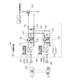
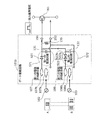
- FIG. 1 is a block diagram showing a configuration of a gate drive circuit 101 according to an embodiment of the present invention.
- the gate drive circuit 101 is a gate drive circuit that drives the gate terminal of the semiconductor switching element 161 (here, an N-type transistor), and includes an output signal terminal 151, an output reference terminal 152, and a first electromagnetic resonance coupler. 107, a second electromagnetic resonance coupler 108, a first rectifier circuit 171, a second rectifier circuit 172, and a pull-down resistor 135.
- the pull-down resistor 135 is not an essential component of the gate drive circuit 101 according to the present invention, but is provided to obtain a stable output signal.
- the second electromagnetic resonance coupler 108 receives the modulated second high-frequency signal (here, the second AC signal 103) indicating the period during which the semiconductor switching element 161 is turned off, and receives the input second It is the 2nd non-contact signal transmitter which transmits and outputs AC signal 103 non-contact.
- the modulated second high-frequency signal here, the second AC signal 103
- the first rectifier circuit 171 rectifies the first AC signal 102 output from the first electromagnetic resonance coupler 107, so that the output signal terminal 151 having the output reference terminal 152 as a reference terminal is connected to the first AC signal 102.
- a rectifier circuit including at least a first diode 121 (here, the first diode 121, the first inductor 181 and the first capacitor 131) that outputs a signal having a voltage of polarity (positive here). It is.
- the first inductor 181 and the first capacitor 131 are not essential components in the gate drive circuit 101 of the present invention, but are provided for more efficient rectification.
- the output signal from the first rectifier circuit 171 is less likely to flow to the second diode 122 than the gate drive circuit in which the first diode 121 and the second diode 122 have the same threshold voltage.
- the first rectifier circuit 171 generates a higher positive output voltage (a signal that turns on the semiconductor switching element 161 more reliably).
- the cathode of the first diode 121 constituting the first rectifier circuit 171 is the first receiving-side resonator 107b constituting the first electromagnetic resonance coupler 107 (that is, the output terminal of the first electromagnetic resonance coupler 107).
- the anode of the first diode 121 constituting the first rectifier circuit 171 is connected to the output reference terminal 152.
- the first AC signal 102 is a signal indicating a period during which the semiconductor switching element 161 is turned on, here, an input signal for supplying a signal power for generating a positive voltage to the output terminal of the gate drive circuit 101 (however, (A high-frequency signal modulated to a frequency that can pass through the first electromagnetic resonance coupler 107). That is, the first AC signal 102 is output as an output voltage such that the voltage at the output signal terminal 151 is positive with respect to the voltage at the output reference terminal 152.
- the frequency of the carrier wave of the first AC signal 102 is designed to be suitable for the transmission frequency (operating frequency or resonance frequency) of the first electromagnetic resonance coupler 107.
- the carrier frequency of the AC signal 103 is designed to match the transmission frequency of the second electromagnetic resonance coupler 108.
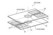
- the first electromagnetic resonance coupler 107 and the second electromagnetic resonance coupler 108 are open ring type electromagnetic resonance couplers as shown in FIG. From the first transmission resonator 107a (second transmission resonator 108a) of the (second electromagnetic resonance coupler 108) to the first reception resonator 107b (second reception resonator 108b). It is designed to transmit a signal having a frequency of 5.8 GHz without contact. Both the first transmitter-side resonator 107a (second transmitter-side resonator 108a) and the first receiver-side resonator 107b (second receiver-side resonator 108b) are open rings formed on a substrate.
- the first electromagnetic resonance coupler 107 and the second electromagnetic resonance coupler 108 are open ring type electromagnetic resonance couplers as shown in FIG. 2, but other shapes (closed ring type) are used. Or a spiral type electromagnetic resonance coupler.
- the first receiving-side resonator 107b is connected to the first rectifier circuit 171 configured by the first diode 121.
- the first diode 121 has its cathode connected to the first receiving resonator 107 b, and its anode connected to the output reference terminal 152 of the gate drive circuit 101. Further, a first inductor 181 is connected between the cathode and the output signal terminal 151.
- the second receiving-side resonator 108b is connected to a second rectifier circuit 172 including a second diode 122 (diode 122a and diode 122b).
- the diode 122a and the diode 122b constituting the second diode 122 are connected in series, and the cathode of the diode 122a and the anode of the diode 122b are connected.
- the diode 122a has an anode connected to the second receiving resonator 108b, and a second inductor 182 connected between the anode and the output signal terminal 151.
- the cathode of the diode 122b and the output signal terminal 151 of the gate drive circuit 101 are connected.
- the anode of the diode 122 a corresponds to the anode of the second diode 122
- the cathode of the diode 122 b corresponds to the cathode of the second diode 122.
- the ground of the first receiving resonator 107b (the ground pattern 20 shown in FIG. 2) is connected to the output reference terminal 152.
- the ground of the second receiving resonator 108b (shown in FIG. 2).
- the ground pattern 20) is connected to the output reference terminal 152.
- first capacitor 131 a first capacitor 131, a second capacitor 132, and a pull-down resistor 135 are connected in parallel between the output signal terminal 151 and the output reference terminal 152.
- the first capacitor 131 and the second capacitor 132 are separate independent capacitors as described above, but may be a single capacitor combined into one.
- first inductor 181 and the first capacitor 131 function as a demodulator that removes the high-frequency signal rectified by the first diode 121, but in this embodiment, the configuration of the first rectifier circuit 171. Treated as an element.
- the second inductor 182 and the second capacitor 132 function as a demodulator that removes the high-frequency signal rectified by the second diode 122, but in this embodiment, the second rectifier circuit 172 Treated as a component.
- the pull-down resistor 135 is an output side of the rectifier circuit (the first rectifier circuit 171 and the second rectifier circuit 172) even when various loads (a load that changes every moment) are connected to the output terminal of the gate drive circuit 101. It plays the role of stabilizing the impedance. As a result, a good output signal can be obtained at the output terminal of the gate drive circuit 101.
- the gate drive circuit 101 operates without the pull-down resistor 135, it is not an essential component for the gate drive circuit 101 according to the present invention.
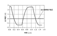
- FIG. 1 shows the waveform of the modulated first AC signal 102, the waveform of the modulated second AC signal 103, and the waveform of the voltage output signal at the output signal terminal 151 relative to the voltage at the output reference terminal 152. .
- Each waveform is a voltage waveform with respect to the elapsed time.
- the waveform of the output signal is a voltage waveform in which the voltage at the output reference terminal 152 is the reference voltage and the output signal terminal 151 is positive.
- the first AC signal 102 indicating the ON period of the semiconductor switching element 161 and the second AC signal 103 indicating the OFF period of the semiconductor switching element 161 are collectively referred to as an input signal to the gate drive circuit 101.
- the first AC signal 102 and the second AC signal 103 are modulated signals obtained by modulating the carrier wave with a low-frequency pulse waveform, and the envelope is a low-frequency pulse waveform (described above). PWM signal). Furthermore, the waveform of the envelope of the first AC signal 102 and the waveform of the envelope of the second AC signal 103 are inverted.
- the first AC signal 102 is input to the first electromagnetic resonance coupler 107. Since the frequency of the carrier wave of the first AC signal 102 is 5.8 GHz, the signal is propagated in a non-contact manner from the input side to the output side via the first electromagnetic resonance coupler 107.
- the first AC signal 102 is transmitted from the first transmitting-side resonator 107a to the first receiving-side resonator 107b with high transmission efficiency due to electromagnetic resonance coupling, and the first receiving-side resonator 107b transmits the first An AC signal 102 is output.
- an electromagnetic resonance coupler is used as a non-contact signal transmitter, and the transmitting resonator and the receiving resonator are strongly coupled. There is very little, and conversely, it is hardly affected by noise. For this reason, a favorable output waveform is obtained.
- the ground in the input side (primary side) circuit with the first electromagnetic resonance coupler 107 as a boundary is connected to the ground pattern 10 of the first transmission side resonator 107a.
- the first AC signal output from the first electromagnetic resonance coupler 107 is input to the first rectifier circuit 171, and subsequently connected to the first inductor 181 and the first capacitor 131,
- the high frequency signal of .8 GHz is rectified (demodulated).
- the high-frequency component is removed and demodulated into a pulse waveform.
- the cathode of the first diode 121 is connected to the output signal terminal 151 via the first inductor 181, and the anode of the first diode 121 is connected to the output reference terminal 152.
- a voltage at which the voltage at the output signal terminal 151 is positive with respect to the voltage at the output reference terminal 152 that is, a voltage for turning on the semiconductor switching element 161 is generated.
- the output signal of the gate drive circuit 101 is a signal that has been transmitted in a non-contact manner via the first electromagnetic resonance coupler 107 that is a non-contact signal transmitter, Is an insulated state, and the voltage at the output reference terminal 152 can be floated from the ground on the input side.
- the first AC signal 102 is provided between the output signal terminal 151 and the output reference terminal 152. The voltage corresponding to can be supplied.
- the gate drive circuit is configured only by a circuit that transmits the ON state of the input signal (the first path including the first electromagnetic resonance coupler 107 and the first rectifier circuit 171), the gate drive is performed.
- the gate voltage can be supplied to the semiconductor switching element 161 connected to the output terminal of the circuit 101, when the input signal is turned off, the supplied gate current (charge accumulated in the gate terminal) can be extracted. Can not.
- a second path constituted by the second electromagnetic resonance coupler 108 and the second rectifier circuit 172 is provided, whereby the output reference terminal 152 is connected to the output reference terminal 152 when the input signal is off.
- electric power with a negative voltage at the output signal terminal 151 is supplied.
- the second AC signal 103 is transmitted to the second rectifier circuit 172 through the second electromagnetic resonance coupler 108 in a non-contact manner.
- the second AC signal 103 output from the second electromagnetic resonance coupler 108 is output by the second rectifier circuit 172, and the second inductor 182 and the second capacitor 132 that are subsequently connected thereto.
- the high frequency signal of 5.8 GHz is rectified (demodulated). In this process, since the second AC signal 103 is envelope-detected, the high-frequency component is removed and demodulated into a low-frequency pulse waveform.
- the first rectifier circuit 171 is composed of one diode (first diode 121), and the second rectifier circuit 172 is composed of two diodes (diode 122a and diode 122b).
- first diode 121 the first diode 121
- second rectifier circuit 172 is composed of two diodes (diode 122a and diode 122b).
- these three diodes all have the same characteristics (the threshold voltage of the on-current is the same).
- the first rectifier circuit 171 When the first AC signal 102 indicates the ON state, the first rectifier circuit 171 generates a positive voltage at the output signal terminal 151 with respect to the output reference terminal 152. However, at this time, a voltage is generated in the forward direction between the cathode and the anode of the second diode 222 of the second rectifier circuit 272. When this voltage becomes equal to or higher than the threshold voltage of the second diode 222, the second A current flows through the diode 222. For this reason, a voltage equal to or higher than the threshold voltage of the second diode 222 cannot be output to the output signal terminal 151.
- the second rectifier circuit 172 as the second diode 122, two diodes 122a and 122b are connected in series, so that the second rectifier The voltage at which current starts to flow through the second diode 122 included in the circuit 172 can be increased. That is, the maximum positive output voltage output from the output terminal of the gate drive circuit 101 can be increased to the sum of the threshold voltage of the diode 122a and the threshold voltage of the diode 122b. In other words, the maximum value of the positive output voltage output from the gate drive circuit 101 is increased by making the diodes constituting the second diode 122 of the second rectifier circuit 172 into multiple stages (two or more stages). be able to.
- the configuration in which the diodes constituting the rectifier circuit are arranged in multiple stages is particularly effective when the gate drive circuit 101 and the semiconductor switching element 161 are integrated.
- the gate drive circuit 101 and the semiconductor switching element 161 are generally manufactured by the same semiconductor manufacturing process, so that the threshold voltage of the gate of the semiconductor switching element 161 and the individual diodes constituting the rectifier circuit are The threshold voltage is equivalent.
- the number of diodes constituting the second rectifier circuit 172 is one, a voltage larger than the threshold voltage of the gate of the semiconductor switching element 161 cannot be supplied. Therefore, in the case where the gate driving circuit 101 is manufactured using an integrated circuit, it is effective to use multiple stages of diodes that form a rectifier circuit.
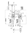
- the second rectifier circuit 472 may be configured by one diode. Even in such a gate drive circuit 101a, when the threshold voltage of the second diode 422 is larger than the threshold voltage of the first diode 121, a higher output voltage is obtained than when the threshold voltages of these diodes are the same. Can supply.
- the gate drive circuit of the present embodiment and its modification can control the output voltage (maximum positive voltage and maximum negative voltage)
- the semiconductor switching element having a low gate drive voltage in particular, Suitable for driving nitride power semiconductor switching elements such as GaN.
- the first rectifier circuit 571 of the gate drive circuit 101b in this modification is composed of a first diode 521 and a first capacitor 131.
- the anode of the first diode 521 and the first receiving resonator 107b of the first electromagnetic resonance coupler 107 are connected, while the cathode of the first diode 521 and the output signal terminal 151 are connected.
- the second rectifier circuit 572 of the gate drive circuit 101b includes a second diode 522 and a second capacitor 132.
- the second diode 522 includes two diodes 522a and 522b connected in series. That is, the anode of the diode 522a and the cathode of the diode 522b are connected.
- the cathode of the second diode 522 (that is, the cathode of the diode 522a) and the second receiving-side resonator 108b of the second electromagnetic resonance coupler 108 are connected, and the anode of the second diode 522 (that is, the diode 522b). Are connected to the output signal terminal 151.
Landscapes
- Engineering & Computer Science (AREA)
- Power Engineering (AREA)
- Power Conversion In General (AREA)
- Electronic Switches (AREA)
Abstract
Priority Applications (2)
| Application Number | Priority Date | Filing Date | Title |
|---|---|---|---|
| JP2013516826A JP5367922B1 (ja) | 2012-01-30 | 2013-01-23 | ゲート駆動回路 |
| US14/007,663 US8847663B2 (en) | 2012-01-30 | 2013-01-23 | Gate drive circuit |
Applications Claiming Priority (2)
| Application Number | Priority Date | Filing Date | Title |
|---|---|---|---|
| JP2012017083 | 2012-01-30 | ||
| JP2012-017083 | 2012-01-30 |
Publications (1)
| Publication Number | Publication Date |
|---|---|
| WO2013114818A1 true WO2013114818A1 (fr) | 2013-08-08 |
Family
ID=48904870
Family Applications (1)
| Application Number | Title | Priority Date | Filing Date |
|---|---|---|---|
| PCT/JP2013/000302 Ceased WO2013114818A1 (fr) | 2012-01-30 | 2013-01-23 | Circuit d'attaque de grille |
Country Status (3)
| Country | Link |
|---|---|
| US (1) | US8847663B2 (fr) |
| JP (1) | JP5367922B1 (fr) |
| WO (1) | WO2013114818A1 (fr) |
Cited By (9)
| Publication number | Priority date | Publication date | Assignee | Title |
|---|---|---|---|---|
| WO2015015709A1 (fr) * | 2013-07-30 | 2015-02-05 | パナソニックIpマネジメント株式会社 | Circuit de réception haute fréquence et dispositif d'émission de signal isolé |
| WO2015029363A1 (fr) * | 2013-08-27 | 2015-03-05 | パナソニックIpマネジメント株式会社 | Circuit d'attaque de grille |
| WO2015059854A1 (fr) * | 2013-10-25 | 2015-04-30 | パナソニックIpマネジメント株式会社 | Appareil de pilotage de gâchette |
| JP2015164291A (ja) * | 2014-01-29 | 2015-09-10 | パナソニックIpマネジメント株式会社 | 信号送信回路、スイッチングシステム、及びマトリックスコンバータ |
| JP2015164290A (ja) * | 2014-01-29 | 2015-09-10 | パナソニックIpマネジメント株式会社 | 半導体デバイス、スイッチングシステム及びマトリックスコンバータ |
| JP2016140065A (ja) * | 2015-01-21 | 2016-08-04 | パナソニック株式会社 | 信号反転装置、電力伝送装置、および、負電圧生成回路 |
| JP2016220210A (ja) * | 2015-05-25 | 2016-12-22 | パナソニックIpマネジメント株式会社 | 信号生成回路 |
| JP2021048680A (ja) * | 2019-09-18 | 2021-03-25 | 国立大学法人静岡大学 | レクテナ装置及びレクテナ装置を設計する方法 |
| US11201606B2 (en) * | 2017-12-08 | 2021-12-14 | Institute Of Geology And Geophysics, The Chinese Academy Of Sciences | CSAMT transmitter |
Families Citing this family (6)
| Publication number | Priority date | Publication date | Assignee | Title |
|---|---|---|---|---|
| CN103339857B (zh) * | 2011-11-01 | 2017-02-15 | 松下知识产权经营株式会社 | 栅极驱动电路 |
| JP5367922B1 (ja) * | 2012-01-30 | 2013-12-11 | パナソニック株式会社 | ゲート駆動回路 |
| CN105103405B (zh) * | 2013-03-27 | 2018-11-27 | 弗莱克森克洛叙有限公司 | 具有可控多个输入整流的供电设备 |
| JP5861055B2 (ja) * | 2013-07-30 | 2016-02-16 | パナソニックIpマネジメント株式会社 | ゲート駆動回路 |
| US10014781B2 (en) | 2016-08-02 | 2018-07-03 | Abb Schweiz Ag | Gate drive systems and methods using wide bandgap devices |
| US12567794B2 (en) * | 2024-06-24 | 2026-03-03 | Hamilton Sundstrand Corporation | Radio frequency integrated gate driver for a power switch device and method |
Citations (4)
| Publication number | Priority date | Publication date | Assignee | Title |
|---|---|---|---|---|
| JPH0362612A (ja) * | 1989-07-31 | 1991-03-18 | Isao Takahashi | ゲートドライブ回路 |
| JPH066967A (ja) * | 1991-08-28 | 1994-01-14 | Matsushita Electric Works Ltd | 自己消孤型素子の駆動回路 |
| US5686854A (en) * | 1996-03-14 | 1997-11-11 | Magl Power Inc. | Isolated driver circuit for high frequency solid-state switches |
| JP2009077104A (ja) * | 2007-09-20 | 2009-04-09 | Nikon Corp | コイル駆動回路 |
Family Cites Families (9)
| Publication number | Priority date | Publication date | Assignee | Title |
|---|---|---|---|---|
| US6132386A (en) * | 1997-07-01 | 2000-10-17 | Neurometrix, Inc. | Methods for the assessment of neuromuscular function by F-wave latency |
| JP3080063B2 (ja) | 1998-04-06 | 2000-08-21 | 日本電気株式会社 | インバータ回路 |
| JP3855116B2 (ja) | 2000-03-22 | 2006-12-06 | 日本光電工業株式会社 | 半導体スイッチ駆動回路 |
| EP2302850A1 (fr) | 2003-04-30 | 2011-03-30 | Analog Devices, Inc. | Isolateurs de signal utilisant des micro-transformateurs |
| JP4676765B2 (ja) | 2005-01-06 | 2011-04-27 | 株式会社トライエンジニアリング | スイッチング回路 |
| KR100777394B1 (ko) | 2006-05-17 | 2007-11-19 | 삼성전자주식회사 | 진폭 불균형을 개선하기 위한 온칩 트랜스포머 밸룬 |
| JP4835334B2 (ja) | 2006-09-06 | 2011-12-14 | 国立大学法人徳島大学 | 高周波信号伝送装置 |
| CN101325376B (zh) * | 2007-06-15 | 2012-05-02 | 力博特公司 | 开关器件的驱动电路 |
| JP5367922B1 (ja) * | 2012-01-30 | 2013-12-11 | パナソニック株式会社 | ゲート駆動回路 |
-
2013
- 2013-01-23 JP JP2013516826A patent/JP5367922B1/ja not_active Expired - Fee Related
- 2013-01-23 US US14/007,663 patent/US8847663B2/en not_active Expired - Fee Related
- 2013-01-23 WO PCT/JP2013/000302 patent/WO2013114818A1/fr not_active Ceased
Patent Citations (4)
| Publication number | Priority date | Publication date | Assignee | Title |
|---|---|---|---|---|
| JPH0362612A (ja) * | 1989-07-31 | 1991-03-18 | Isao Takahashi | ゲートドライブ回路 |
| JPH066967A (ja) * | 1991-08-28 | 1994-01-14 | Matsushita Electric Works Ltd | 自己消孤型素子の駆動回路 |
| US5686854A (en) * | 1996-03-14 | 1997-11-11 | Magl Power Inc. | Isolated driver circuit for high frequency solid-state switches |
| JP2009077104A (ja) * | 2007-09-20 | 2009-04-09 | Nikon Corp | コイル駆動回路 |
Cited By (10)
| Publication number | Priority date | Publication date | Assignee | Title |
|---|---|---|---|---|
| WO2015015709A1 (fr) * | 2013-07-30 | 2015-02-05 | パナソニックIpマネジメント株式会社 | Circuit de réception haute fréquence et dispositif d'émission de signal isolé |
| WO2015029363A1 (fr) * | 2013-08-27 | 2015-03-05 | パナソニックIpマネジメント株式会社 | Circuit d'attaque de grille |
| WO2015059854A1 (fr) * | 2013-10-25 | 2015-04-30 | パナソニックIpマネジメント株式会社 | Appareil de pilotage de gâchette |
| JP2015164291A (ja) * | 2014-01-29 | 2015-09-10 | パナソニックIpマネジメント株式会社 | 信号送信回路、スイッチングシステム、及びマトリックスコンバータ |
| JP2015164290A (ja) * | 2014-01-29 | 2015-09-10 | パナソニックIpマネジメント株式会社 | 半導体デバイス、スイッチングシステム及びマトリックスコンバータ |
| JP2016140065A (ja) * | 2015-01-21 | 2016-08-04 | パナソニック株式会社 | 信号反転装置、電力伝送装置、および、負電圧生成回路 |
| JP2016220210A (ja) * | 2015-05-25 | 2016-12-22 | パナソニックIpマネジメント株式会社 | 信号生成回路 |
| US11201606B2 (en) * | 2017-12-08 | 2021-12-14 | Institute Of Geology And Geophysics, The Chinese Academy Of Sciences | CSAMT transmitter |
| JP2021048680A (ja) * | 2019-09-18 | 2021-03-25 | 国立大学法人静岡大学 | レクテナ装置及びレクテナ装置を設計する方法 |
| JP7290219B2 (ja) | 2019-09-18 | 2023-06-13 | 国立大学法人静岡大学 | レクテナ装置及びレクテナ装置を設計する方法 |
Also Published As
| Publication number | Publication date |
|---|---|
| US8847663B2 (en) | 2014-09-30 |
| US20140009202A1 (en) | 2014-01-09 |
| JPWO2013114818A1 (ja) | 2015-05-11 |
| JP5367922B1 (ja) | 2013-12-11 |
Similar Documents
| Publication | Publication Date | Title |
|---|---|---|
| JP5367922B1 (ja) | ゲート駆動回路 | |
| JP6083648B2 (ja) | ゲート駆動回路 | |
| US9438230B2 (en) | Gate drive circuit | |
| JP5866506B2 (ja) | ゲート駆動回路 | |
| JP6544580B2 (ja) | 高周波受信回路及び絶縁型信号伝送装置 | |
| US9362963B2 (en) | Radio-frequency signal reception circuit and isolated signal transmission apparatus | |
| US20170117815A1 (en) | Voltage isolator | |
| RU2565664C1 (ru) | Способ управления в системах беспроводной передачи мощности | |
| US20170207706A1 (en) | Wireless power-feeding apparatus | |
| US9438231B2 (en) | Gate drive circuit | |
| US9634655B2 (en) | Drive device having first and second switching devices with different gate widths | |
| CN115833411A (zh) | 用于无线功率接收的装置、控制电路以及传输的通信方法 | |
| JP2018170610A (ja) | 電磁共鳴結合器及びこれを用いたゲート駆動回路、信号伝送装置 | |
| JP4915438B2 (ja) | ワイヤレス給電装置およびワイヤレス電力伝送システム | |
| CN106165284A (zh) | 谐振型高频电源装置及谐振型高频电源装置用开关电路 | |
| JP2016140065A (ja) | 信号反転装置、電力伝送装置、および、負電圧生成回路 | |
| Hosotani | Importance of High Power/High Frequency CS-devices on Wireless Power Supply Using Direct Current Resonance System |
Legal Events
| Date | Code | Title | Description |
|---|---|---|---|
| ENP | Entry into the national phase |
Ref document number: 2013516826 Country of ref document: JP Kind code of ref document: A |
|
| 121 | Ep: the epo has been informed by wipo that ep was designated in this application |
Ref document number: 13743108 Country of ref document: EP Kind code of ref document: A1 |
|
| WWE | Wipo information: entry into national phase |
Ref document number: 14007663 Country of ref document: US |
|
| NENP | Non-entry into the national phase |
Ref country code: DE |
|
| 122 | Ep: pct application non-entry in european phase |
Ref document number: 13743108 Country of ref document: EP Kind code of ref document: A1 |