WO2013118615A1 - Système optique de formation d'une image réfléchissante, appareil d'exposition et procédé de fabrication d'un dispositif - Google Patents
Système optique de formation d'une image réfléchissante, appareil d'exposition et procédé de fabrication d'un dispositif Download PDFInfo
- Publication number
- WO2013118615A1 WO2013118615A1 PCT/JP2013/051961 JP2013051961W WO2013118615A1 WO 2013118615 A1 WO2013118615 A1 WO 2013118615A1 JP 2013051961 W JP2013051961 W JP 2013051961W WO 2013118615 A1 WO2013118615 A1 WO 2013118615A1
- Authority
- WO
- WIPO (PCT)
- Prior art keywords
- optical system
- reflecting mirror
- reflection
- light
- reflecting
- Prior art date
- Legal status (The legal status is an assumption and is not a legal conclusion. Google has not performed a legal analysis and makes no representation as to the accuracy of the status listed.)
- Ceased
Links
Images



Classifications
-
- H—ELECTRICITY
- H10—SEMICONDUCTOR DEVICES; ELECTRIC SOLID-STATE DEVICES NOT OTHERWISE PROVIDED FOR
- H10P—GENERIC PROCESSES OR APPARATUS FOR THE MANUFACTURE OR TREATMENT OF DEVICES COVERED BY CLASS H10
- H10P76/00—Manufacture or treatment of masks on semiconductor bodies, e.g. by lithography or photolithography
- H10P76/20—Manufacture or treatment of masks on semiconductor bodies, e.g. by lithography or photolithography of masks comprising organic materials
- H10P76/204—Manufacture or treatment of masks on semiconductor bodies, e.g. by lithography or photolithography of masks comprising organic materials of organic photoresist masks
- H10P76/2041—Photolithographic processes
-
- G—PHYSICS
- G03—PHOTOGRAPHY; CINEMATOGRAPHY; ANALOGOUS TECHNIQUES USING WAVES OTHER THAN OPTICAL WAVES; ELECTROGRAPHY; HOLOGRAPHY
- G03F—PHOTOMECHANICAL PRODUCTION OF TEXTURED OR PATTERNED SURFACES, e.g. FOR PRINTING, FOR PROCESSING OF SEMICONDUCTOR DEVICES; MATERIALS THEREFOR; ORIGINALS THEREFOR; APPARATUS SPECIALLY ADAPTED THEREFOR
- G03F7/00—Photomechanical, e.g. photolithographic, production of textured or patterned surfaces, e.g. printing surfaces; Materials therefor, e.g. comprising photoresists; Apparatus specially adapted therefor
- G03F7/70—Microphotolithographic exposure; Apparatus therefor
- G03F7/70058—Mask illumination systems
- G03F7/702—Reflective illumination, i.e. reflective optical elements other than folding mirrors, e.g. extreme ultraviolet [EUV] illumination systems
-
- G—PHYSICS
- G02—OPTICS
- G02B—OPTICAL ELEMENTS, SYSTEMS OR APPARATUS
- G02B17/00—Systems with reflecting surfaces, with or without refracting elements
- G02B17/02—Catoptric systems, e.g. image erecting and reversing system
- G02B17/06—Catoptric systems, e.g. image erecting and reversing system using mirrors only, i.e. having only one curved mirror
- G02B17/0647—Catoptric systems, e.g. image erecting and reversing system using mirrors only, i.e. having only one curved mirror using more than three curved mirrors
- G02B17/0657—Catoptric systems, e.g. image erecting and reversing system using mirrors only, i.e. having only one curved mirror using more than three curved mirrors off-axis or unobscured systems in which all of the mirrors share a common axis of rotational symmetry
-
- G—PHYSICS
- G02—OPTICS
- G02B—OPTICAL ELEMENTS, SYSTEMS OR APPARATUS
- G02B19/00—Condensers, e.g. light collectors or similar non-imaging optics
- G02B19/0004—Condensers, e.g. light collectors or similar non-imaging optics characterised by the optical means employed
- G02B19/0019—Condensers, e.g. light collectors or similar non-imaging optics characterised by the optical means employed having reflective surfaces only (e.g. louvre systems, systems with multiple planar reflectors)
- G02B19/0023—Condensers, e.g. light collectors or similar non-imaging optics characterised by the optical means employed having reflective surfaces only (e.g. louvre systems, systems with multiple planar reflectors) at least one surface having optical power
-
- G—PHYSICS
- G02—OPTICS
- G02B—OPTICAL ELEMENTS, SYSTEMS OR APPARATUS
- G02B19/00—Condensers, e.g. light collectors or similar non-imaging optics
- G02B19/0033—Condensers, e.g. light collectors or similar non-imaging optics characterised by the use
- G02B19/0095—Condensers, e.g. light collectors or similar non-imaging optics characterised by the use for use with ultraviolet radiation
-
- G—PHYSICS
- G03—PHOTOGRAPHY; CINEMATOGRAPHY; ANALOGOUS TECHNIQUES USING WAVES OTHER THAN OPTICAL WAVES; ELECTROGRAPHY; HOLOGRAPHY
- G03F—PHOTOMECHANICAL PRODUCTION OF TEXTURED OR PATTERNED SURFACES, e.g. FOR PRINTING, FOR PROCESSING OF SEMICONDUCTOR DEVICES; MATERIALS THEREFOR; ORIGINALS THEREFOR; APPARATUS SPECIALLY ADAPTED THEREFOR
- G03F7/00—Photomechanical, e.g. photolithographic, production of textured or patterned surfaces, e.g. printing surfaces; Materials therefor, e.g. comprising photoresists; Apparatus specially adapted therefor
- G03F7/70—Microphotolithographic exposure; Apparatus therefor
- G03F7/70216—Mask projection systems
- G03F7/70233—Optical aspects of catoptric systems, i.e. comprising only reflective elements, e.g. extreme ultraviolet [EUV] projection systems
Definitions
- the present invention relates to a reflection imaging optical system, an exposure apparatus, and a device manufacturing method. More specifically, the present invention relates to a reflective imaging optical system suitable for an exposure apparatus that transfers a circuit pattern on a mask onto a photosensitive substrate by using, for example, EUV light by a mirror projection method.
- An EUVL (Extreme UltraViolet Lithography) exposure apparatus that uses EUV (Extreme UltraViolet) light having a wavelength of about 5 to 40 nm, for example, has attracted attention as an exposure apparatus used for manufacturing semiconductor elements and the like.
- EUV light When EUV light is used as the exposure light, there is no transmissive optical material and refractive optical material that can be used. Therefore, a reflective mask is used, and a reflective optical system (an optical system composed only of a reflective member) is used as a projection optical system. Will be used.
- a reflection imaging optical system having an entrance pupil on the optical system side with the object plane sandwiched is referred to as a “positive pupil type reflection imaging optical system”, and “an optical system with the object plane sandwiched”.
- the “reflective imaging optical system having an entrance pupil on the opposite side” is referred to as an “inverted pupil type reflective imaging optical system”.
- An aspect of the present invention has been made in view of the above-described problems, and provides a reflective imaging optical system that can suppress the footprint of the apparatus when applied to, for example, an exposure apparatus that uses EUV light.
- a plurality of reflecting mirrors including a first reflecting mirror that reflects light reflected by the first surface first and a second reflecting mirror that reflects second; A region where the light from the illumination optical system irradiates the first surface is an irradiated region, and a portion where the irradiated region is located on the first surface is predetermined with respect to the optical axes of the plurality of reflecting mirrors.
- the reflection region of the first reflection mirror and the reflection region of the second reflection mirror are located on the predetermined direction side with respect to the optical axes of the plurality of reflection mirrors,
- a reflection imaging optical system is provided in which the first reflecting mirror and the second reflecting mirror are arranged so as to sandwich an optical path of light from the illumination optical system.
- a plurality of light beams including a first reflecting mirror that reflects light reflected on the first surface first, a second reflecting mirror that reflects second light, and a third reflecting mirror that reflects third light.
- the first reflecting mirror and the second reflecting mirror are arranged so that the reflecting area of the first reflecting mirror and the reflecting area of the second reflecting mirror sandwich the optical path of light from the illumination optical system, A region where the light from the illumination optical system irradiates the first surface is an irradiated region, and a portion where the irradiated region is located on the first surface is predetermined with respect to the optical axes of the plurality of reflecting mirrors.
- the third reflecting mirror is disposed closer to the predetermined direction than the optical axis of the plurality of reflecting mirrors.
- an illumination optical system that illuminates the pattern of the first surface with light from a light source, and the reflection of the first or second embodiment that projects the pattern onto a photosensitive substrate installed on the second surface.
- An image forming optical system is provided.
- the fourth embodiment using the exposure apparatus of the third embodiment, exposing the predetermined pattern to the photosensitive substrate; Developing the photosensitive substrate having the predetermined pattern transferred thereon, and forming a mask layer having a shape corresponding to the predetermined pattern on the surface of the photosensitive substrate; And processing the surface of the photosensitive substrate through the mask layer.
- a device manufacturing method is provided.
- FIG. 1 shows schematically the structure of the exposure apparatus concerning embodiment. It is a figure which shows the positional relationship of the arc-shaped effective imaging area
- FIG. 1 is a view schematically showing a configuration of an exposure apparatus according to the embodiment.
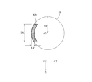
- FIG. 2 is a diagram showing the positional relationship between the arc-shaped effective imaging region formed on the wafer and the optical axis.
- the Y axis is set in a direction parallel to the paper surface of FIG. 1
- the X axis is set in the direction perpendicular to the paper surface of FIG.
- the first direction and the predetermined direction are, for example, directions parallel to the Y axis (Y axis direction).
- a light source 1 for supplying exposure light includes, for example, a laser plasma X-ray source.
- a discharge plasma light source or another X-ray source can be used.
- the light emitted from the light source 1 enters the illumination optical system IL via a wavelength selection filter (not shown) arranged as necessary.
- the wavelength selection filter has a characteristic of selectively transmitting only EUV light having a predetermined wavelength (for example, 13.4 nm) from light supplied from the light source 1 and blocking transmission of other wavelength light.
- EUV light that has passed through the wavelength selection filter is guided to an optical integrator 2 including a pair of fly-eye optical systems (fly-eye mirrors) 2a and 2b.
- an optical integrator 2 including a pair of fly-eye optical systems (fly-eye mirrors) 2a and 2b.
- a multilayer film that reflects only EUV light having a predetermined wavelength may be formed on the reflection surface of a mirror that reflects or condenses the generated EUV light.
- the wavelength selection filter since the wavelength selection filter is not necessary, the light source 1 can be reduced in size. Further, it is possible to prevent the light quantity loss of EUV light in the wavelength selection filter.
- the first fly's eye optical system 2a has a plurality of first reflection optical elements arranged in parallel, and the second fly's eye optical system 2b corresponds to the plurality of first reflection optical elements of the first fly's eye optical system 2a.
- the first fly's eye optical system 2a is configured by, for example, arranging a large number of concave mirror elements having an arcuate outer shape vertically and horizontally
- the second fly's eye optical system 2b has, for example, a rectangular outer shape.
- a plurality of concave mirror elements are arranged vertically and horizontally and densely.
- the detailed configuration and operation of the fly-eye optical systems 2a and 2b can be used with the aid of, for example, US Patent Application Publication No. 2002 / 0093636A1.
- a substantial surface light source having a predetermined shape is formed in the vicinity of the reflecting surface of the second fly's eye optical system 2b.
- This substantial surface light source is formed at the exit pupil position of the illumination optical system IL including the pair of fly-eye optical systems 2a and 2b.
- the exit pupil position of the illumination optical system IL (that is, the position in the vicinity of the reflection surface of the second fly's eye optical system 2b) coincides with the position of the entrance pupil of the inverse pupil type reflection imaging optical system (projection optical system) 6. Yes.
- the light from the substantial surface light source that is, the light emitted from the optical integrator 2 is incident on the flat mirror 3 that functions as an oblique incidence mirror.
- the light reflected by the flat mirror 3 passes between the first reflecting mirror M1 and the second reflecting mirror M2 of the reflective imaging optical system 6 and is then arranged substantially parallel and close to the reflective mask 4.
- An arcuate illumination area is formed on the mask 4 through an arcuate opening (light transmission part) of the field stop (not shown).
- the optical integrator 2 (2a, 2b) and the flat mirror 3 constitute an illumination optical system IL for Koehler illumination of the mask 4 provided with a predetermined pattern by the light from the light source 1.
- a reflecting mirror having power is not arranged in the optical path between the second fly's eye optical system 2b and the mask 4.
- the power of the reflecting mirror is the reciprocal of the focal length of the reflecting mirror.
- a reflecting mirror having power may be arranged in the optical path between the second fly's eye optical system 2b and the mask 4.
- the mask 4 is held by a mask stage 5 movable along the Y direction so that the pattern surface extends along the XY plane.
- the movement of the mask stage 5 is measured by a laser interferometer or an encoder (not shown).
- On the mask 4 for example, an arcuate illumination region symmetric with respect to the Y axis is formed.
- the illuminated light from the mask 4 forms a pattern image of the mask 4 on the wafer 7 which is a photosensitive substrate via the reflective imaging optical system 6.
- an arc-shaped effective imaging region (stationary exposure region) ER that is symmetrical with respect to the Y-axis is formed on the wafer 7.
- a circular region (image circle) IF having a radius Y0 centered on the optical axis AX
- the length in the X direction is LX
- the length in the Y direction is in contact with the image circle IF.
- An arc-shaped effective imaging region ER of LY is formed.
- the arc-shaped effective imaging region ER is a part of a ring-shaped region centered on the optical axis AX
- the length LY is along the direction connecting the center of the arc-shaped effective imaging region ER and the optical axis. This is the width dimension of the effective imaging region ER.
- the wafer 7 is held by a wafer stage 8 that can move two-dimensionally along the X and Y directions so that the exposure surface extends along the XY plane.
- the movement of the wafer stage 8 is measured by a laser interferometer or an encoder (not shown) as in the mask stage 5.
- scanning exposure scanning exposure
- the mask stage 5 and the wafer stage 8 are moved along the Y direction, that is, while the mask 4 and the wafer 7 are moved relative to the reflective imaging optical system 6 along the Y direction.
- the moving speed of the wafer stage 8 is set to 1/8 of the moving speed of the mask stage 5 to perform synchronous scanning. Further, by repeating the scanning exposure while moving the wafer stage 8 two-dimensionally along the X direction and the Y direction, the pattern of the mask 4 is sequentially transferred to each exposure region of the wafer 7.
- the projection magnification of the reflective imaging optical system 6 may be 1/6, 1/4, or the like.
- the moving speed of the wafer stage 8 is set to 1/6 of the moving speed of the mask stage 5
- the projection magnification of the reflective imaging optical system 6 is If it is 1/4, the moving speed of the wafer stage 8 is set to 1/4 of the moving speed of the mask stage 5.
- the reflective imaging optical system 6 has a pattern surface (hereinafter, referred to as “pattern surface”) of the mask 4 along a single optical axis AX extending linearly as shown in FIGS.
- a first reflective optical system G1 that forms an intermediate image of the pattern at a position optically conjugate with the mask 4
- a final reduced image (intermediate image) of the pattern of the mask 4 is transferred to the transfer surface of the wafer 7.
- wafer surface also referred to as “wafer surface” and a second reflective optical system G2 formed thereon. That is, a position optically conjugate with the illumination area on the pattern surface of the mask 4 is formed in the optical path between the first reflective optical system G1 and the second reflective optical system G2.
- the reflective imaging optical system 6 may be configured by only the first reflective optical system G1, or may be configured by using a plurality of optical systems such as a third reflective optical system and a fourth reflective optical system. .
- the first reflecting optical system G1 has a first reflecting mirror M1 having a concave reflecting surface and a second reflecting surface having a convex reflecting surface in the order of incidence of light (in order of reflection from the mask 4 toward the wafer 7).
- a reflecting mirror M2 a third reflecting mirror M3 having a concave or convex reflecting surface, a fourth reflecting mirror M4 having a concave reflecting surface, and a fifth reflecting mirror M5 having a convex reflecting surface;
- a sixth reflecting mirror M6 having a concave reflecting surface is used.
- the second reflecting optical system G2 is configured by a seventh reflecting mirror M7 having a convex reflecting surface and an eighth reflecting mirror M8 having a concave reflecting surface in the light incident order.
- the reflecting surface of each of the reflecting mirrors M1 to M8 may be a reflecting surface having a concave shape, a convex shape, a flat shape, or another curved shape.
- an aperture stop AS (not shown) is provided at the position of the reflecting surface of the fourth reflecting mirror M4 or in the vicinity thereof.
- the aperture stop AS sets the numerical aperture of the reflective imaging optical system 6 by limiting the light flux of the exposure light.
- the aperture stop AS is composed of a variable aperture stop that can adjust the size of the opening, and a diaphragm switching member that includes a plurality of openings having different sizes and shapes and can be switched to a desired opening. Also good.
- the light from the illumination area that is away from the optical axis AX on the ⁇ Y direction side on the pattern surface (first surface) of the mask 4 is reflected by the reflecting surface of the first reflecting mirror M1 and the second reflecting mirror M2.
- the intermediate image of the mask pattern after being sequentially reflected by the surface, the reflecting surface of the third reflecting mirror M3, the reflecting surface of the fourth reflecting mirror M4, the reflecting surface of the fifth reflecting mirror M5, and the reflecting surface of the sixth reflecting mirror M6 Form.
- the light from the intermediate image formed through the first reflecting optical system G1 is sequentially reflected by the reflecting surface of the seventh reflecting mirror M7 and the reflecting surface of the eighth reflecting mirror M8, and then the surface of the wafer 7 (second A reduced image of the mask pattern is formed in the effective imaging region ER that is distant from the optical axis AX to the ⁇ Y direction side on the surface).
- the magnitude of the imaging magnification of the reflective imaging optical system 6 according to the first example is 1/8
- the magnitude of the imaging magnification of the reflective imaging optical system 6 according to the second example is 1/6. Therefore, in the first embodiment, a reduced image that is 1/8 times the mask pattern is formed in the effective image formation region ER, and in the second embodiment, a reduced image that is 1/6 times the mask pattern is formed in the effective image formation region ER. Is done.
- the eight reflecting mirrors M1 to M8 constituting the reflective imaging optical system 6 are installed so that the center of curvature of the reflecting surface is positioned on the linear optical axis AX. Further, the reflecting mirrors M1 to M8 have aspherical reflecting surfaces formed along a rotationally symmetric surface with respect to the optical axis AX. When the reflecting surface is aspherical, the paraxial center of curvature can be used as the center of curvature of the reflecting surface.
- the aspherical surface In the vicinity of the intersection of the rotationally symmetric axis and the aspherical surface, the aspherical surface can be regarded as a spherical surface, and the center of curvature in this spherical surface is called the paraxial curvature center (vertex curvature center).
- the reflective imaging optical system 6 may be composed of 7 to 12 reflecting mirrors.
- the reflective imaging optical system 6 of each embodiment is an optical system that is almost telecentric on the wafer side (image side).
- the principal ray reaching each position on the image plane of the reflective imaging optical system 6 is substantially perpendicular to the image plane. With this configuration, good image formation is possible even if the wafer has irregularities within the depth of focus of the reflective imaging optical system 6.
- the reflective imaging optical system 6 according to each embodiment is an inverted pupil type reflective imaging optical system having an entrance pupil at a position a predetermined distance away from the reflective imaging optical system 6 across the mask 4. .
- the light reflected by the flat mirror 3 of the illumination optical system IL passes between the first reflecting mirror M1 and the second reflecting mirror M2, and then on the mask 4 from the optical axis AX in the ⁇ Y direction.
- An arcuate illumination area separated from the side is formed. That is, the first reflecting mirror M1 and the second reflecting mirror M2 are arranged so as to sandwich the optical path of the light from the illumination optical system IL. Further, the reflection region of the first reflecting mirror M1 and the reflection region of the second reflecting mirror M2 are located on the ⁇ Y direction side of the optical axis AX.
- the “reflection area” may mean an irradiation area of light formed on the reflection surface of the reflection mirror by the light incident on the reflection mirror.
- the maximum irradiation area can be regarded as a “reflection area”.
- the area when there are a plurality of light irradiation areas formed on the reflecting surface of the reflecting mirror by light incident on the reflecting mirror, the area includes a plurality of irradiation areas on the reflecting surface and the area thereof is The smallest region may be regarded as a “reflection region”.
- the first reflecting mirror M1 to the third reflecting mirror M3 are positioned on the ⁇ Y direction side with respect to the optical axis AX, and the reflection region of the first reflecting mirror M1 is the reflection of the second reflecting mirror M2. It is formed farther from the optical axis AX than the region.
- the angle formed between the optical path of the light incident on the flat mirror 3 of the illumination optical system IL and the optical axis AX of the reflection imaging optical system 6 can be suppressed to a small value.
- the size of the footprint (installation area) of the EUV exposure apparatus along the scanning direction can be kept small, and as a result, costs relating to the manufacture and installation of the apparatus can be reduced.
- the surface where the reflecting surface of the flat mirror 3 is extended and the pattern surface of the mask 4 are provided. It is preferable to set the angle which is an acute angle among the angles formed by the positioned plane to 60 degrees or more.
- the size of the imaging magnification of the reflective imaging optical system 6 is set to a normal level. This is facilitated by setting a value smaller than 1/4, for example, 1/8 or 1/6. This is because the cross section of the light beam incident on the first reflecting mirror M1 and the second reflecting mirror M2 when the imaging magnification is reduced while the image-side numerical aperture of the reflective imaging optical system 6 is secured to a required size. This is because the distance between the first reflecting mirror M1 and the second reflecting mirror M2 can be secured large.
- the incident angle of the light beam to the flat mirror 3 can be made larger than that of the prior art, so that the reflectivity at the flat mirror 3 can be ensured larger than that of the prior art, and the light quantity at the flat mirror 3 is consequently expanded. Loss can be kept small.
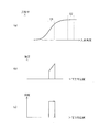
- the incident angle of the light beam on the flat mirror 3 is larger than that of the related art, the illuminance unevenness in the Y direction in the illumination area on the mask 4 can be suppressed small as shown in FIG.
- FIG. 5A is a diagram showing the incident angle characteristic of the reflectance of the flat mirror.
- the reflectivity changes relatively greatly depending on the incident angle.
- the illuminance unevenness in the Y direction in the illumination area is relatively large.
- the flat mirror 3 is used for a light beam in a range 52 having a relatively large incident angle as in the present embodiment, the reflectance becomes almost constant without depending on the incident angle. )
- the illuminance unevenness in the Y direction in the illumination area is suppressed to a small level.
- the reflective surface of the flat mirror is formed of a single layer or a multilayer film, and a flat mirror having various incident angle characteristics can be used by adjusting the number of layers, film thickness, film material, etc. Can do.
- the interval along the Y direction between the reflection region M1a of the first reflection mirror M1 and the reflection region M2a of the second reflection mirror M2 is H, and the first reflection mirror M1.
- the cross-sectional dimension along the Y direction of the reflective region M1a is D, the following conditional expression (1) may be satisfied. 0.5 ⁇ D / H ⁇ 1.1 (1)
- conditional expression (1) When the lower limit value of conditional expression (1) is not reached, light incident on the mask 4 at a position where the cross-sectional dimension D is relatively small, that is, a position relatively close to the mask 4, is between the first reflecting mirror M1 and the second reflecting mirror M2. Since it passes through, the second reflecting mirror M2 may be too close to the mask 4 to be difficult to place. Alternatively, since the interval H becomes relatively large, and the incident angle of the light beam to the mask 4 and the incident angle of the light beam to the first reflecting mirror M1 are increased, the reflectance at the mask 4 and the first reflecting mirror M1 decreases. As a result, there is a risk that the throughput of the apparatus may be reduced due to a light amount loss in the mask 4 and the first reflecting mirror M1.
- the pattern may not be accurately imaged on the exposure surface of the wafer 7 due to the unevenness of the pattern of the mask 4. .
- the imaging performance is deteriorated due to the shadow caused by the unevenness of the pattern, or the pattern 4 is incident on the mask 4 due to the unevenness of the pattern
- a light amount loss due to light being blocked can be cited.
- conditional expression (1) If the upper limit value of conditional expression (1) is exceeded, the incident light on the mask 4 may interfere with the first reflecting mirror M1 and the second reflecting mirror M2. Therefore, when the conditional expression (1) is satisfied, a space can be secured between the mask 4 and the second reflecting mirror M2, and the arrangement of the first reflecting mirror M1 and the second reflecting mirror M2 can be easily performed. There are advantages that can be done.
- the conditional expression (1) When the conditional expression (1) is satisfied, the incident angle of the light beam on the mask 4 and the incident angle of the light beam on the first reflecting mirror M1 can be reduced. Therefore, the reflectivity of the mask 4 and the first reflecting mirror M1 can be reduced. The decrease can be suppressed, and the throughput of the exposure apparatus is improved.
- conditional expression (1) when the conditional expression (1) is satisfied, the incident angle of the light beam on the mask 4 and the incident angle of the light beam on the first reflecting mirror M1 can be reduced.
- the pattern image of the mask 4 can be accurately formed on the exposed surface of the wafer 7.
- the influence that the incident light on the mask 4 interferes with the first reflecting mirror M1 and the second reflecting mirror M2 can be suppressed.
- the lower limit value of conditional expression (1) may be set to 0.75.
- the lower limit value of conditional expression (1) may be set to 0.9.
- the cross-sectional dimension D may be a dimension along the Y direction of a region obtained by projecting the reflection region M1a of the first reflecting mirror M1 onto a plane orthogonal to the optical axis.
- the cross-sectional dimension D is along the Y direction of the region occupied by the light incident on the pattern surface of the mask 4 on the optical axis orthogonal plane (indicated by a broken line extending horizontally in FIG. 6) including the position of the first reflecting mirror M1. It is good also as a dimension.
- the position of the first reflecting mirror M1 may be a position closest to the optical axis among the peripheral portions of the reflecting region M1a of the first reflecting mirror M1, and among the peripheral portions of the reflecting region M1a of the first reflecting mirror M1. It may be a position farthest from the optical axis.
- the aspherical surface is along the optical axis from the tangential plane at the apex of the aspherical surface to the position on the aspherical surface at the height y, where y is the height perpendicular to the optical axis.
- the distance (sag amount) is z
- the apex radius of curvature is r
- the cone coefficient is ⁇
- the n-th aspherical coefficient is C n
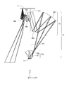
- FIG. 3 is a diagram showing a configuration of the reflective imaging optical system according to the first example of the present embodiment.
- the light from the mask 4 is a concave reflecting surface of the first reflecting mirror M1, a convex reflecting surface of the second reflecting mirror M2,
- the concave reflecting surface of the third reflecting mirror M3, the concave reflecting surface of the fourth reflecting mirror M4, the convex reflecting surface of the fifth reflecting mirror M5, and the concave reflecting surface of the sixth reflecting mirror M6 are sequentially arranged. After being reflected, an intermediate image of the mask pattern is formed.
- the light from the intermediate image formed through the first reflecting optical system G1 is sequentially reflected by the convex reflecting surface of the seventh reflecting mirror M7 and the concave reflecting surface of the eighth reflecting mirror M8, and then the wafer.
- a reduced image (secondary image) of the mask pattern is formed on 7.
- the imaging magnification size ⁇ of the reflective imaging optical system 6 is 1/8, and the angle formed by the extended surface of the reflective surface of the flat mirror 3 and the mask surface is the acute angle. The angle is 82 degrees.
- an aperture stop AS (not shown) is disposed at the position of the reflecting surface of the fourth reflecting mirror M4 or in the vicinity thereof.
- the aperture stop AS is located between the third reflecting mirror M3 and the fourth reflecting mirror M4, between the fourth reflecting mirror M4 and the fifth reflecting mirror M5, or at a position conjugate with the reflecting surface of the fourth reflecting mirror M4. You may provide in places, such as the position of the vicinity.
- the following table (1) lists the values of the specifications of the reflective imaging optical system according to the first example.
- ⁇ is the wavelength of exposure light
- ⁇ is the size of the imaging magnification
- NA is the numerical aperture on the image side (wafer side)
- Y0 is the image on the wafer 7.
- the radius of the circle IF maximum image height
- LX the dimension along the X direction of the effective imaging area ER
- LY the dimension along the Y direction of the effective imaging area ER (arc-shaped effective imaging area ER ) (Width dimension) respectively.
- the surface number is the progression of light from the mask surface (pattern surface of the mask 4) that is the object surface to the wafer surface (transfer surface of the wafer 7) that is the image surface.
- the order of the reflecting surfaces from the mask side along the direction to be performed r is the apex radius of curvature (center radius of curvature: mm) of each reflecting surface, and d is the on-axis interval of each reflecting surface, ie, the surface interval (mm). Show. Note that the surface distance d changes its sign each time it is reflected.
- the curvature radius of the convex surface toward the mask side is positive and the curvature radius of the concave surface is negative regardless of the incident direction of the light beam.
- H is the distance along the Y direction between the reflection region of the first reflection mirror M1 and the reflection region of the second reflection mirror M2, and D is the first reflection mirror.
- the cross-sectional dimensions along the Y direction of the reflective area of M1 are respectively shown.
- PD is a distance along the optical axis between the entrance pupil and the mask surface (incidence pupil distance)
- TT is a distance along the optical axis between the mask surface and the wafer surface (full length).
- R represents the incident angle (rad) of the principal ray incident on the mask surface.
- the incident angle R takes a negative value when the principal ray reflected by the mask surface goes in a direction away from the optical axis AX.
- the above notation is the same in the following table (2).
- the maximum value is obtained.
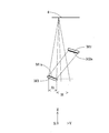
- FIG. 4 is a diagram showing a configuration of the reflective imaging optical system according to the second example of the present embodiment.
- the light from the mask 4 is a concave reflecting surface of the first reflecting mirror M1, a convex reflecting surface of the second reflecting mirror M2,
- the convex reflecting surface of the third reflecting mirror M3, the concave reflecting surface of the fourth reflecting mirror M4, the convex reflecting surface of the fifth reflecting mirror M5, and the concave reflecting surface of the sixth reflecting mirror M6 are sequentially arranged. After being reflected, an intermediate image of the mask pattern is formed.
- the light from the intermediate image formed through the first reflecting optical system G1 is sequentially reflected by the convex reflecting surface of the seventh reflecting mirror M7 and the concave reflecting surface of the eighth reflecting mirror M8, and then the wafer.
- a reduced image of the mask pattern is formed on 7.
- the imaging magnification size ⁇ of the reflective imaging optical system 6 is 1/6, and the angle formed by the extended surface of the reflective surface of the flat mirror 3 and the mask surface is the acute angle. The angle is 83 degrees.
- an aperture stop AS (not shown) is disposed at the position of the reflecting surface of the fourth reflecting mirror M4 or in the vicinity thereof.
- Table (2) lists the values of the specifications of the reflective imaging optical system according to the second example.
- EUV light having a wavelength of 13.4 nm is used as an example.
- the present invention is not limited to this.
- EUV light having a wavelength of about 5 to 40 nm other The present invention can be similarly applied to a reflection imaging optical system using light of an appropriate wavelength.
- the reflective imaging optical system 6 includes eight reflecting mirrors M1 to M8 in which the centers of curvature of the reflecting surfaces are arranged on the same axis (on the optical axis AX). However, at least one of the eight reflecting mirrors M1 to M8 may be installed such that the center of curvature of the reflecting surface deviates from the optical axis AX. In each of the above-described embodiments, all the reflecting mirrors M1 to M8 have reflecting surfaces formed along a plane that is infinitely rotationally symmetric with respect to the optical axis AX. Of the reflecting mirrors M1 to M8, At least one of these may have a reflecting surface formed along a plane that is rotationally finite times (for example, once, twice, and three times).
- the present invention is applied to an inverted pupil type reflection imaging optical system.
- the present invention is not limited to the inverted pupil type, and can be applied to the normal pupil type reflective imaging optical system.
- the entrance pupil is located on the optical system side with respect to the object plane.
- the reflective area of the first reflective mirror M1 and the reflective area of the second reflective mirror M2 are formed on the mask M with respect to the optical axis AX of the reflective imaging optical system 6.
- the first reflecting mirror M1 and the second reflecting mirror M2 are located on the same side as the irradiated area (illumination area) on the pattern surface, and are arranged so as to sandwich the optical path of the light from the illumination optical system IL.
- the angle formed by the optical path of the light incident on the flat mirror 3 of the illumination optical system IL and the optical axis AX of the reflection imaging optical system 6 can be suppressed to 82 to 83 degrees, and as a result, the footprint of the exposure apparatus. Can be kept small.
- EUV light is used as exposure light. Therefore, the pattern of the mask M and the pattern of the mask M to be transferred and the wafer W are moved relative to the reflective imaging optical system 6. It is possible to perform projection exposure on the wafer W with high resolution. As a result, a highly accurate device can be manufactured under good exposure conditions using a scanning exposure apparatus having a large resolving power.
- the exposure apparatus of the above-described embodiment is manufactured by assembling various subsystems including the respective constituent elements recited in the claims of the present application so as to maintain predetermined mechanical accuracy, electrical accuracy, and optical accuracy. Is done.
- various optical systems are adjusted to achieve optical accuracy
- various mechanical systems are adjusted to achieve mechanical accuracy
- various electrical systems are Adjustments are made to achieve electrical accuracy.
- the assembly process from the various subsystems to the exposure apparatus includes mechanical connection, electrical circuit wiring connection, pneumatic circuit piping connection and the like between the various subsystems. Needless to say, there is an assembly process for each subsystem before the assembly process from the various subsystems to the exposure apparatus. When the assembly process of the various subsystems to the exposure apparatus is completed, comprehensive adjustment is performed to ensure various accuracies as the entire exposure apparatus.
- the exposure apparatus may be manufactured in a clean room where the temperature, cleanliness, etc. are controlled.
- FIG. 7 is a flowchart showing a semiconductor device manufacturing process.
- a metal film is vapor-deposited on a wafer W to be a semiconductor device substrate (step S40), and a photoresist, which is a photosensitive material, is applied on the vapor-deposited metal film. (Step S42).
- the pattern formed on the mask (reticle) M is transferred to each shot area on the wafer W (step S44: exposure process), and the transfer of the wafer W after the transfer is completed.
- step S46 development process
- step S48 processing step
- the resist pattern is a photoresist layer in which unevenness having a shape corresponding to the pattern transferred by the exposure apparatus of the above-described embodiment is generated, and the recess penetrates the photoresist layer. is there.
- the surface of the wafer W is processed through this resist pattern.
- the processing performed in step S48 includes, for example, at least one of etching of the surface of the wafer W or film formation of a metal film or the like.
- the exposure apparatus of the above-described embodiment performs pattern transfer using the wafer W coated with the photoresist as a photosensitive substrate.
- a laser plasma X-ray source is used as a light source for supplying EUV light.
- the present invention is not limited to this, and for example, synchrotron radiation (SOR) light is used as EUV light. You can also.
- the present invention is applied to an exposure apparatus having a light source for supplying EUV light.
- the present invention is not limited to this, and a light source that supplies light having a wavelength other than EUV light.
- the present invention can also be applied to an exposure apparatus having
- variable pattern forming apparatus that dynamically forms a predetermined pattern based on predetermined electronic data can be used.
- a variable pattern forming apparatus for example, a spatial light modulator including a plurality of reflecting elements driven based on predetermined electronic data can be used.
- An exposure apparatus using a spatial light modulator as a variable pattern forming apparatus is disclosed in, for example, US Patent Publication Nos. 2007/0296936 and 2009/0122381.
- teachings of US Patent Publication Nos. 2007/0296936 and 2009/0122381 are incorporated by reference.
- the present invention is applied to the reflective imaging optical system as the projection optical system of the exposure apparatus.
- the present invention is not limited to this.
- the present invention can be similarly applied to a reflective imaging optical system that forms an image on the second surface.
Landscapes
- Physics & Mathematics (AREA)
- General Physics & Mathematics (AREA)
- Optics & Photonics (AREA)
- Exposure And Positioning Against Photoresist Photosensitive Materials (AREA)
- Lenses (AREA)
- Exposure Of Semiconductors, Excluding Electron Or Ion Beam Exposure (AREA)
- Microscoopes, Condenser (AREA)
Abstract
Priority Applications (6)
| Application Number | Priority Date | Filing Date | Title |
|---|---|---|---|
| KR1020147024449A KR102330570B1 (ko) | 2012-02-06 | 2013-01-30 | 반사 결상 광학계, 노광 장치, 및 디바이스 제조 방법 |
| JP2013557471A JP6135514B2 (ja) | 2012-02-06 | 2013-01-30 | 反射結像光学系、およびデバイス製造方法 |
| US14/451,699 US9541842B2 (en) | 2012-02-06 | 2014-08-05 | Reflective image-forming optical system, exposure apparatus, and device manufacturing method |
| US15/401,202 US10025195B2 (en) | 2012-02-06 | 2017-01-09 | Reflective image-forming optical system, exposure apparatus, and device manufacturing method |
| US16/008,576 US10599042B2 (en) | 2012-02-06 | 2018-06-14 | Reflective image-forming optical system, exposure apparatus, and device manufacturing method |
| US16/783,628 US10976669B2 (en) | 2012-02-06 | 2020-02-06 | Reflective image-forming optical system, exposure apparatus, and device manufacturing method |
Applications Claiming Priority (2)
| Application Number | Priority Date | Filing Date | Title |
|---|---|---|---|
| JP2012023167 | 2012-02-06 | ||
| JP2012-023167 | 2012-02-06 |
Related Child Applications (1)
| Application Number | Title | Priority Date | Filing Date |
|---|---|---|---|
| US14/451,699 Continuation US9541842B2 (en) | 2012-02-06 | 2014-08-05 | Reflective image-forming optical system, exposure apparatus, and device manufacturing method |
Publications (1)
| Publication Number | Publication Date |
|---|---|
| WO2013118615A1 true WO2013118615A1 (fr) | 2013-08-15 |
Family
ID=48947381
Family Applications (1)
| Application Number | Title | Priority Date | Filing Date |
|---|---|---|---|
| PCT/JP2013/051961 Ceased WO2013118615A1 (fr) | 2012-02-06 | 2013-01-30 | Système optique de formation d'une image réfléchissante, appareil d'exposition et procédé de fabrication d'un dispositif |
Country Status (4)
| Country | Link |
|---|---|
| US (4) | US9541842B2 (fr) |
| JP (4) | JP6135514B2 (fr) |
| KR (1) | KR102330570B1 (fr) |
| WO (1) | WO2013118615A1 (fr) |
Families Citing this family (1)
| Publication number | Priority date | Publication date | Assignee | Title |
|---|---|---|---|---|
| WO2013118615A1 (fr) | 2012-02-06 | 2013-08-15 | 株式会社ニコン | Système optique de formation d'une image réfléchissante, appareil d'exposition et procédé de fabrication d'un dispositif |
Citations (3)
| Publication number | Priority date | Publication date | Assignee | Title |
|---|---|---|---|---|
| WO2006033336A1 (fr) * | 2004-09-22 | 2006-03-30 | Nikon Corporation | Appareil d’eclairage, appareil d’exposition et procede de fabrication de microdispositif |
| WO2009125530A1 (fr) * | 2008-04-09 | 2009-10-15 | 株式会社ニコン | Dispositif de source de lumière, dispositif d'exposition et procédé de fabrication |
| JP2011086708A (ja) * | 2009-10-14 | 2011-04-28 | Nikon Corp | 絞り装置、光学系、露光装置、及び電子デバイスの製造方法 |
Family Cites Families (31)
| Publication number | Priority date | Publication date | Assignee | Title |
|---|---|---|---|---|
| US5956192A (en) * | 1997-09-18 | 1999-09-21 | Svg Lithography Systems, Inc. | Four mirror EUV projection optics |
| JP4238390B2 (ja) | 1998-02-27 | 2009-03-18 | 株式会社ニコン | 照明装置、該照明装置を備えた露光装置および該露光装置を用いて半導体デバイスを製造する方法 |
| JP2000091209A (ja) | 1998-09-14 | 2000-03-31 | Nikon Corp | 露光装置の製造方法、露光装置、及びデバイス製造方法 |
| JP2000098229A (ja) | 1998-09-22 | 2000-04-07 | Nikon Corp | 反射縮小投影光学系、該光学系を備えた投影露光装置および該装置を用いた露光方法 |
| US6109756A (en) | 1998-09-21 | 2000-08-29 | Nikon Corporation | Catoptric reduction projection optical system |
| JP4134544B2 (ja) | 2001-10-01 | 2008-08-20 | 株式会社ニコン | 結像光学系および露光装置 |
| US7348575B2 (en) * | 2003-05-06 | 2008-03-25 | Nikon Corporation | Projection optical system, exposure apparatus, and exposure method |
| US7161735B2 (en) * | 2003-09-02 | 2007-01-09 | Canon Kabushiki Kaisha | Projection optical system, exposure apparatus and device fabricating method |
| DE102005042005A1 (de) | 2004-12-23 | 2006-07-06 | Carl Zeiss Smt Ag | Hochaperturiges Objektiv mit obskurierter Pupille |
| JP4858439B2 (ja) | 2005-01-25 | 2012-01-18 | 株式会社ニコン | 露光装置及び露光方法並びにマイクロデバイスの製造方法 |
| EP1856578B1 (fr) | 2005-03-08 | 2010-05-19 | Carl Zeiss SMT AG | Systeme de projection pour microlithographie a diaphragme accessible ou butee d'ouverture |
| WO2007023665A1 (fr) * | 2005-08-24 | 2007-03-01 | Nikon Corporation | Système optique de projection, appareil d’exposition et procédé de fabrication de dispositif |
| JP2009508150A (ja) | 2005-09-13 | 2009-02-26 | カール・ツァイス・エスエムティー・アーゲー | マイクロリソグラフィ投影光学系、ある機器を製造するための方法、光学面を設計する方法 |
| DE102006014380A1 (de) | 2006-03-27 | 2007-10-11 | Carl Zeiss Smt Ag | Projektionsobjektiv und Projektionsbelichtungsanlage mit negativer Schnittweite der Eintrittspupille |
| EP2005250B1 (fr) | 2006-04-07 | 2012-11-07 | Carl Zeiss SMT GmbH | Système optique de projection pour microlithographie, outil et procédé de production |
| EP2045645A1 (fr) | 2006-07-06 | 2009-04-08 | Nikon Corporation | Micro-actionneur, unité optique, dispositif d'exposition et procédé de fabrication |
| JP5885098B2 (ja) | 2007-09-21 | 2016-03-15 | カール・ツァイス・エスエムティー・ゲーエムベーハー | マイクロリソグラフィ用の掩蔽瞳を有する投影対物系 |
| DE102008033340B3 (de) | 2008-07-16 | 2010-04-08 | Carl Zeiss Smt Ag | Abbildende Optik |
| DE102008046699B4 (de) | 2008-09-10 | 2014-03-13 | Carl Zeiss Smt Gmbh | Abbildende Optik |
| WO2010032753A1 (fr) * | 2008-09-18 | 2010-03-25 | 株式会社ニコン | Diaphragme, système optique, appareil d'exposition et procédé de fabrication de dispositif électronique |
| JP2010205795A (ja) | 2009-02-27 | 2010-09-16 | Nikon Corp | 光源装置、露光装置及びデバイスの製造方法 |
| JP5810467B2 (ja) | 2009-03-06 | 2015-11-11 | カール・ツァイス・エスエムティー・ゲーエムベーハー | 結像光学系及び該結像光学系を有するマイクロリソグラフィ用の投影露光装置 |
| US8743342B2 (en) | 2009-11-17 | 2014-06-03 | Nikon Corporation | Reflective imaging optical system, exposure apparatus, and method for producing device |
| KR102290738B1 (ko) * | 2009-11-24 | 2021-08-18 | 가부시키가이샤 니콘 | 결상 광학계, 노광 장치 및 디바이스 제조 방법 |
| EP2513697B1 (fr) | 2009-12-14 | 2019-08-07 | Carl Zeiss SMT GmbH | Elément optique de formation d'image |
| JP2011150227A (ja) * | 2010-01-25 | 2011-08-04 | Nikon Corp | 露光装置、およびデバイス製造方法 |
| KR102160046B1 (ko) * | 2010-04-02 | 2020-09-28 | 가부시키가이샤 니콘 | 조명 광학계, 노광 방법 및 디바이스 제조 방법 |
| JP2011228536A (ja) | 2010-04-21 | 2011-11-10 | Nikon Corp | 反射光学部材、光学系、露光装置及びデバイスの製造方法 |
| US9075322B2 (en) | 2010-09-10 | 2015-07-07 | Nikon Corporation | Reflective imaging optical system, exposure apparatus, and method for producing device |
| DE102010062763A1 (de) | 2010-12-09 | 2012-06-14 | Carl Zeiss Smt Gmbh | Verfahren zum Vermessen eines optischen Systems |
| WO2013118615A1 (fr) * | 2012-02-06 | 2013-08-15 | 株式会社ニコン | Système optique de formation d'une image réfléchissante, appareil d'exposition et procédé de fabrication d'un dispositif |
-
2013
- 2013-01-30 WO PCT/JP2013/051961 patent/WO2013118615A1/fr not_active Ceased
- 2013-01-30 KR KR1020147024449A patent/KR102330570B1/ko active Active
- 2013-01-30 JP JP2013557471A patent/JP6135514B2/ja active Active
-
2014
- 2014-08-05 US US14/451,699 patent/US9541842B2/en active Active
-
2017
- 2017-01-09 US US15/401,202 patent/US10025195B2/en active Active
- 2017-04-26 JP JP2017087344A patent/JP6365723B2/ja active Active
-
2018
- 2018-06-14 US US16/008,576 patent/US10599042B2/en active Active
- 2018-06-28 JP JP2018122931A patent/JP6551869B2/ja active Active
-
2019
- 2019-07-01 JP JP2019122855A patent/JP6931469B2/ja active Active
-
2020
- 2020-02-06 US US16/783,628 patent/US10976669B2/en active Active
Patent Citations (3)
| Publication number | Priority date | Publication date | Assignee | Title |
|---|---|---|---|---|
| WO2006033336A1 (fr) * | 2004-09-22 | 2006-03-30 | Nikon Corporation | Appareil d’eclairage, appareil d’exposition et procede de fabrication de microdispositif |
| WO2009125530A1 (fr) * | 2008-04-09 | 2009-10-15 | 株式会社ニコン | Dispositif de source de lumière, dispositif d'exposition et procédé de fabrication |
| JP2011086708A (ja) * | 2009-10-14 | 2011-04-28 | Nikon Corp | 絞り装置、光学系、露光装置、及び電子デバイスの製造方法 |
Also Published As
| Publication number | Publication date |
|---|---|
| KR102330570B1 (ko) | 2021-11-25 |
| JP2017161921A (ja) | 2017-09-14 |
| JP6365723B2 (ja) | 2018-08-01 |
| US10976669B2 (en) | 2021-04-13 |
| US10599042B2 (en) | 2020-03-24 |
| US20200174375A1 (en) | 2020-06-04 |
| US20170115574A1 (en) | 2017-04-27 |
| US20180299781A1 (en) | 2018-10-18 |
| JP2018185520A (ja) | 2018-11-22 |
| JP6551869B2 (ja) | 2019-07-31 |
| US9541842B2 (en) | 2017-01-10 |
| JP6135514B2 (ja) | 2017-05-31 |
| JP2019168728A (ja) | 2019-10-03 |
| US10025195B2 (en) | 2018-07-17 |
| US20150085270A1 (en) | 2015-03-26 |
| JP6931469B2 (ja) | 2021-09-08 |
| JPWO2013118615A1 (ja) | 2015-05-11 |
| KR20140123556A (ko) | 2014-10-22 |
Similar Documents
| Publication | Publication Date | Title |
|---|---|---|
| US11467501B2 (en) | Image-forming optical system, exposure apparatus, and device producing method | |
| US7483122B2 (en) | Projection optical system, exposure apparatus, and exposure method | |
| JP5888585B2 (ja) | 反射結像光学系、露光装置、およびデバイス製造方法 | |
| JP5682248B2 (ja) | 反射結像光学系、露光装置、およびデバイス製造方法 | |
| JP6551869B2 (ja) | 照明光学系、露光装置、およびデバイス製造方法 | |
| WO2010052961A1 (fr) | Système optique d’imagerie, appareil d’exposition et procédé de fabrication d’un dispositif | |
| JP2009258461A (ja) | 結像光学系、露光装置、およびデバイス製造方法 |
Legal Events
| Date | Code | Title | Description |
|---|---|---|---|
| 121 | Ep: the epo has been informed by wipo that ep was designated in this application |
Ref document number: 13747148 Country of ref document: EP Kind code of ref document: A1 |
|
| ENP | Entry into the national phase |
Ref document number: 2013557471 Country of ref document: JP Kind code of ref document: A |
|
| NENP | Non-entry into the national phase |
Ref country code: DE |
|
| ENP | Entry into the national phase |
Ref document number: 20147024449 Country of ref document: KR Kind code of ref document: A |
|
| 122 | Ep: pct application non-entry in european phase |
Ref document number: 13747148 Country of ref document: EP Kind code of ref document: A1 |