WO2013121729A1 - Module de charge sans contact et terminal mobile le comprenant - Google Patents
Module de charge sans contact et terminal mobile le comprenant Download PDFInfo
- Publication number
- WO2013121729A1 WO2013121729A1 PCT/JP2013/000553 JP2013000553W WO2013121729A1 WO 2013121729 A1 WO2013121729 A1 WO 2013121729A1 JP 2013000553 W JP2013000553 W JP 2013000553W WO 2013121729 A1 WO2013121729 A1 WO 2013121729A1
- Authority
- WO
- WIPO (PCT)
- Prior art keywords
- coil
- nfc
- charging
- charging module
- charging coil
- Prior art date
- Legal status (The legal status is an assumption and is not a legal conclusion. Google has not performed a legal analysis and makes no representation as to the accuracy of the status listed.)
- Ceased
Links
Images





Classifications
-
- H—ELECTRICITY
- H01—ELECTRIC ELEMENTS
- H01Q—ANTENNAS, i.e. RADIO AERIALS
- H01Q7/00—Loop antennas with a substantially uniform current distribution around the loop and having a directional radiation pattern in a plane perpendicular to the plane of the loop
- H01Q7/06—Loop antennas with a substantially uniform current distribution around the loop and having a directional radiation pattern in a plane perpendicular to the plane of the loop with core of ferromagnetic material
-
- H—ELECTRICITY
- H01—ELECTRIC ELEMENTS
- H01F—MAGNETS; INDUCTANCES; TRANSFORMERS; SELECTION OF MATERIALS FOR THEIR MAGNETIC PROPERTIES
- H01F38/00—Adaptations of transformers or inductances for specific applications or functions
- H01F38/14—Inductive couplings
-
- H—ELECTRICITY
- H01—ELECTRIC ELEMENTS
- H01Q—ANTENNAS, i.e. RADIO AERIALS
- H01Q1/00—Details of, or arrangements associated with, antennas
- H01Q1/12—Supports; Mounting means
- H01Q1/22—Supports; Mounting means by structural association with other equipment or articles
- H01Q1/24—Supports; Mounting means by structural association with other equipment or articles with receiving set
- H01Q1/241—Supports; Mounting means by structural association with other equipment or articles with receiving set used in mobile communications, e.g. GSM
- H01Q1/242—Supports; Mounting means by structural association with other equipment or articles with receiving set used in mobile communications, e.g. GSM specially adapted for hand-held use
- H01Q1/243—Supports; Mounting means by structural association with other equipment or articles with receiving set used in mobile communications, e.g. GSM specially adapted for hand-held use with built-in antennas
-
- H—ELECTRICITY
- H01—ELECTRIC ELEMENTS
- H01Q—ANTENNAS, i.e. RADIO AERIALS
- H01Q1/00—Details of, or arrangements associated with, antennas
- H01Q1/36—Structural form of radiating elements, e.g. cone, spiral, umbrella; Particular materials used therewith
- H01Q1/38—Structural form of radiating elements, e.g. cone, spiral, umbrella; Particular materials used therewith formed by a conductive layer on an insulating support
-
- H—ELECTRICITY
- H01—ELECTRIC ELEMENTS
- H01Q—ANTENNAS, i.e. RADIO AERIALS
- H01Q1/00—Details of, or arrangements associated with, antennas
- H01Q1/52—Means for reducing coupling between antennas; Means for reducing coupling between an antenna and another structure
- H01Q1/521—Means for reducing coupling between antennas; Means for reducing coupling between an antenna and another structure reducing the coupling between adjacent antennas
-
- H—ELECTRICITY
- H01—ELECTRIC ELEMENTS
- H01Q—ANTENNAS, i.e. RADIO AERIALS
- H01Q21/00—Antenna arrays or systems
- H01Q21/28—Combinations of substantially independent non-interacting antenna units or systems
-
- H—ELECTRICITY
- H02—GENERATION; CONVERSION OR DISTRIBUTION OF ELECTRIC POWER
- H02J—ELECTRIC POWER NETWORKS; CIRCUIT ARRANGEMENTS OR SYSTEMS FOR SUPPLYING OR DISTRIBUTING ELECTRIC POWER; SYSTEMS FOR STORING ELECTRIC ENERGY
- H02J50/00—Circuit arrangements or systems for wireless supply or distribution of electric power
- H02J50/005—Mechanical details of housing or structure aiming to accommodate the power transfer means, e.g. mechanical integration of coils, antennas or transducers into emitting or receiving devices
-
- H—ELECTRICITY
- H02—GENERATION; CONVERSION OR DISTRIBUTION OF ELECTRIC POWER
- H02J—ELECTRIC POWER NETWORKS; CIRCUIT ARRANGEMENTS OR SYSTEMS FOR SUPPLYING OR DISTRIBUTING ELECTRIC POWER; SYSTEMS FOR STORING ELECTRIC ENERGY
- H02J50/00—Circuit arrangements or systems for wireless supply or distribution of electric power
- H02J50/10—Circuit arrangements or systems for wireless supply or distribution of electric power using inductive coupling
- H02J50/12—Circuit arrangements or systems for wireless supply or distribution of electric power using inductive coupling of the resonant type
-
- H—ELECTRICITY
- H02—GENERATION; CONVERSION OR DISTRIBUTION OF ELECTRIC POWER
- H02J—ELECTRIC POWER NETWORKS; CIRCUIT ARRANGEMENTS OR SYSTEMS FOR SUPPLYING OR DISTRIBUTING ELECTRIC POWER; SYSTEMS FOR STORING ELECTRIC ENERGY
- H02J50/00—Circuit arrangements or systems for wireless supply or distribution of electric power
- H02J50/10—Circuit arrangements or systems for wireless supply or distribution of electric power using inductive coupling
-
- H—ELECTRICITY
- H02—GENERATION; CONVERSION OR DISTRIBUTION OF ELECTRIC POWER
- H02J—ELECTRIC POWER NETWORKS; CIRCUIT ARRANGEMENTS OR SYSTEMS FOR SUPPLYING OR DISTRIBUTING ELECTRIC POWER; SYSTEMS FOR STORING ELECTRIC ENERGY
- H02J50/00—Circuit arrangements or systems for wireless supply or distribution of electric power
- H02J50/90—Circuit arrangements or systems for wireless supply or distribution of electric power involving detection or optimisation of position, e.g. alignment
-
- H—ELECTRICITY
- H02—GENERATION; CONVERSION OR DISTRIBUTION OF ELECTRIC POWER
- H02J—ELECTRIC POWER NETWORKS; CIRCUIT ARRANGEMENTS OR SYSTEMS FOR SUPPLYING OR DISTRIBUTING ELECTRIC POWER; SYSTEMS FOR STORING ELECTRIC ENERGY
- H02J7/00—Circuit arrangements for charging or discharging batteries or for supplying loads from batteries
-
- H—ELECTRICITY
- H02—GENERATION; CONVERSION OR DISTRIBUTION OF ELECTRIC POWER
- H02J—ELECTRIC POWER NETWORKS; CIRCUIT ARRANGEMENTS OR SYSTEMS FOR SUPPLYING OR DISTRIBUTING ELECTRIC POWER; SYSTEMS FOR STORING ELECTRIC ENERGY
- H02J7/00—Circuit arrangements for charging or discharging batteries or for supplying loads from batteries
- H02J7/40—Circuit arrangements for charging or discharging batteries or for supplying loads from batteries characterised by the exchange of charge or discharge related data
- H02J7/42—Circuit arrangements for charging or discharging batteries or for supplying loads from batteries characterised by the exchange of charge or discharge related data with electronic devices having internal batteries, e.g. mobile phones
-
- H—ELECTRICITY
- H02—GENERATION; CONVERSION OR DISTRIBUTION OF ELECTRIC POWER
- H02J—ELECTRIC POWER NETWORKS; CIRCUIT ARRANGEMENTS OR SYSTEMS FOR SUPPLYING OR DISTRIBUTING ELECTRIC POWER; SYSTEMS FOR STORING ELECTRIC ENERGY
- H02J7/00—Circuit arrangements for charging or discharging batteries or for supplying loads from batteries
- H02J7/70—Circuit arrangements for charging or discharging batteries or for supplying loads from batteries characterised by the mechanical construction
- H02J7/731—Circuit arrangements for charging or discharging batteries or for supplying loads from batteries characterised by the mechanical construction specially adapted for holding portable devices containing batteries
-
- Y—GENERAL TAGGING OF NEW TECHNOLOGICAL DEVELOPMENTS; GENERAL TAGGING OF CROSS-SECTIONAL TECHNOLOGIES SPANNING OVER SEVERAL SECTIONS OF THE IPC; TECHNICAL SUBJECTS COVERED BY FORMER USPC CROSS-REFERENCE ART COLLECTIONS [XRACs] AND DIGESTS
- Y02—TECHNOLOGIES OR APPLICATIONS FOR MITIGATION OR ADAPTATION AGAINST CLIMATE CHANGE
- Y02E—REDUCTION OF GREENHOUSE GAS [GHG] EMISSIONS, RELATED TO ENERGY GENERATION, TRANSMISSION OR DISTRIBUTION
- Y02E60/00—Enabling technologies; Technologies with a potential or indirect contribution to GHG emissions mitigation
- Y02E60/10—Energy storage using batteries
Definitions
- the present invention relates to a contactless charging module including a contactless charging module and an NFC antenna, and a portable terminal including the contactless charging module.
- a NFC antenna module is provided with a magnetic sheet that improves the efficiency of 13.56 MHz band communication.
- a contactless charging module in a communication device and perform the charging method of the communication device by contactless charging. This is a power transmission coil on the charger side, a power reception coil on the communication device side, and electromagnetic induction is generated between both coils in the band of about 100 kHz to 200 kHz to transmit power from the charger to the communication device side. It is.
- the non-contact charging module is provided with a magnetic sheet that improves the communication efficiency in the band of about 100 kHz to 200 kHz, and is a non-contact charging module.
- NFC is a short-range wireless communication that performs communication by electromagnetic induction using a frequency of 13.56 MHz band.
- power is transmitted by electromagnetic induction using a frequency in the range of about 100 kHz to 200 kHz. Therefore, the optimum magnetic sheet for improving the efficiency of communication (power transmission) in each frequency band differs between the NFC module and the non-contact charging module.
- both the NFC module and the non-contact charging module perform communication (power transmission) by electromagnetic induction, they tend to interfere with each other.
- both coils are wound in a flat shape to increase the opening area. As a result, there is a possibility that the other module takes away the magnetic flux during communication of one module, and an eddy current may be generated in the other coil to weaken the electromagnetic induction of one module.
- each of the NFC module and the non-contact charging module is provided with a magnetic sheet, and each is arranged as a module.
- miniaturization of the communication device is hindered.
- the communication directions are changed so as not to interfere with each other's communication, and the communication surface changes depending on the type of communication, which is very inconvenient.
- smartphones that use most of one surface of the housing as a display unit. When applied to a smartphone, one communication must be performed on the display unit side.
- the object of the present invention is to achieve downsizing by making the non-contact charging coil and the NFC antenna into one module, and in order to prevent mutual interference, the antenna axial direction is different, but communication in the same direction and It is an object to provide a non-contact charging module capable of transmitting power and a portable terminal including the same.
- a contactless charging module includes a charging coil around which a conductive wire is wound, and an NFC coil disposed around the charging coil, and the shaft of the charging coil and the winding of the NFC coil.
- the rotation axis is configured to intersect each other.
- the non-contact charging coil and the NFC antenna are made into a single module to achieve miniaturization, and in order to prevent mutual interference, communication in the same direction can be performed while changing the coil axis direction of the antenna.
- a non-contact charging module that enables power transmission and a portable terminal including the same can be obtained.
- FIG. 1 Schematic of the non-contact charging module in the embodiment of the present invention
- the invention of the present disclosure includes a charging coil around which a conducting wire is wound, and an NFC coil disposed around the charging coil, and the axis of the charging coil and the winding axis of the NFC coil intersect each other.
- This is a non-contact charging module that achieves downsizing by making the contact charging coil and NFC antenna into one module, and in the same direction while changing the coil axis direction of the antenna in order to prevent mutual interference It is possible to obtain a contactless charging module that enables communication and power transmission.
- the charging coil axis and the NFC coil axis are substantially orthogonal to each other, thereby preventing the mutual interference most.
- the contactless charging module includes a plurality of the NFC coils, and the plurality of NFC modules are disposed so as to sandwich the contactless charging module. Mutual interference can be prevented.
- the charging coil is wound in a rectangular shape, and at least two of the NFC coils are arranged along two opposing sides of the rectangular charging coil.
- the NFC communication possible area can be expanded in a balanced manner around the contactless charging module.
- the contactless charging module of the present disclosure includes a magnetic sheet having a surface on which the entire charging coil is placed, and the NFC coil is disposed outside the magnetic sheet, thereby efficiently communicating the NFC coil. Can do well.
- the contactless charging module of the present disclosure includes a magnetic sheet having a surface on which the entire charging coil is placed, and winds the NFC coil around a magnetic core, thereby generating a large amount of power over a short distance.
- the entire contactless charging module can be made thinner and smaller while ensuring a large opening for the charging coil to be transmitted.
- the magnetic sheet and the magnetic core are made of different materials, so that a charging coil that transmits a large amount of power over a short distance and a small amount over a long distance.
- the NFC coil that transmits power and communicates with each other can improve the intended effect by using a magnetic material suitable for each.
- the magnetic sheet and the magnetic core are made of different types of ferrite, so that a charging coil that transmits a large amount of power between distances and a long distance
- the target effect can be greatly improved by the ferrite material suitable for the NFC coil that transmits and communicates with a small electric power.
- the overall thickness in the stacking direction of the charging coil and the magnetic sheet is larger than the thickness of the NFC coil in the same direction, so that the NFC coil disposed on the outside is more By forming it thin, it is possible to effectively reduce the overall size and thickness.
- the length of the two opposing sides of the rectangular charging coil is shorter than the length of the NFC coil in the same direction, so that the magnetic field generated by the NFC coil is reduced. It can be made difficult to be disturbed by the charging coil.
- the number of turns of the charging coil is larger than the number of turns of the NFC coil, so that the inductance value of the charging coil that transmits higher power can be improved.
- the opening surface of the charging coil is larger than the opening surface of the NFC coil, so that the inductance value of the charging coil that transmits higher power can be improved.
- the contactless charging module of the present disclosure since the number of turns of the plurality of NFC coils is equal, a magnetic field is generated in a balanced manner from the plurality of NFC coils, so that NFC communication can be performed stably.
- the plurality of NFC coils have the same shape, so that magnetic fields are generated in a balanced manner from the plurality of NFC coils, so that NFC communication can be performed stably.
- the mobile terminal of the present disclosure is a mobile terminal characterized in that the non-contact charging module of the present disclosure is provided in a housing, and is small by making the contact charging coil and the NFC antenna into one module.
- the non-contact charging module that enables communication and power transmission in the same direction while changing the coil axis direction of the antenna in order to achieve mutualization and prevent mutual interference can be obtained.
- a metal body is provided in the housing, and the NFC coil is disposed at an end portion of the metal body, so that the magnetic field generated by the NFC antenna can be tilted. NFC communication can be performed efficiently.
- the opening of the NFC coil is substantially perpendicular to the metal body, thereby suppressing eddy currents generated in the metal body to the NFC antenna and more efficiently performing NFC communication. It can be performed.
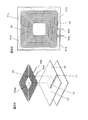
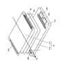
- FIG. 1 is a schematic diagram of a contactless charging module according to an embodiment of the present invention.
- FIG. 1A is a top view of the contactless charging module, and
- FIG. 1B is a perspective view of the contactless charging module.
- the non-contact charging module 100 includes a charging coil 30 in which a conductive wire is wound in a planar shape, two NFC coils 40 arranged around the charging coil 30, and a magnetic sheet that supports the charging coil 30. 10.
- the number of NFC coils 40 may be one, three, four, or more.
- the non-contact charging module 100 includes a sheet-like magnetic sheet 10 having an upper surface and a lower surface facing each other, and the charging coil 30 is placed (adhered) on the upper surface of the magnetic sheet 10. At least one, preferably a plurality of NFC coils 40 are arranged around the magnetic sheet 10 and the charging coil 30. In the present embodiment, two NFC coils 40 facing each other with the magnetic sheet 10 and the charging coil 30 in between are provided. The NFC coil 40 may be placed on the upper surface of the magnetic sheet 10. The coil axes of the two NFC coils 40 are substantially parallel to each other (may intersect at an angle of about ⁇ 10 to +10 degrees), but may be in a substantially vertical or inclined relationship with each other.
- the NFC coil 40 is preferably wound around the magnetic body 20, thereby improving the communication efficiency of the NFC coil 40.
- the area of the upper surface of one magnetic body 20 is smaller than the area of the upper surface of the magnetic sheet 10.
- the coil axis A of the charging coil 30 and the coil axis B of the NFC coil 40 intersect with each other substantially at right angles (about 75 to 105 degrees).
- the magnetic sheet 10 and the magnetic body 20 are in contact via a protective tape or the like, but may be separated from each other. By being in contact with each other, the magnetic sheet 10 and the magnetic body 20 can be maximized in the miniaturized non-contact charging module 100.
- FIG. 2 is a schematic view of a charging coil and a magnetic sheet in the embodiment of the present invention.
- FIG. 2A is an exploded view showing an arrangement relationship between the charging coil and the magnetic sheet
- FIG. 2B is a top view of the charging coil and the magnetic sheet.
- the charging coil 30 is wound in a substantially square shape, but may have any shape such as a substantially rectangular shape including a substantially rectangular shape, a circular shape, an elliptical shape, or a polygonal shape.
- the charging coil 30 has two leg portions (terminals) 32a and 32b as the start and end, and about 8 to 15 lead wires or a plurality of wires (preferably 0.08 mm to 0.00 mm) having a wire diameter of about 0.1 mm. 2 to 15 conductors of 3 mm) are wound around the hollow portion so as to draw a vortex on the surface.
- a coil wound with a litz wire consisting of 12 conductors having a wire diameter of 0.1 mm has much higher AC resistance due to the skin effect than a coil wound with one conductor having the same cross-sectional area. Go down. If the AC resistance during the operation of the coil decreases, the heat generated by the coil decreases, and the charging coil 30 with good thermal characteristics can be obtained.
- the power transmission efficiency can be improved by using a litz wire composed of 8 to 15 conductive wires of 0.08 mm to 1.5 mm. If it is a single wire, it may be a conducting wire having a wire diameter of 0.2 mm to 1 mm. Further, for example, three 0.2 mm conducting wires and two 0.3 mm conducting wires may be used to form one conducting wire like a litz wire. Further, the legs 32 a and 32 b as current supply units supply current from a commercial power source that is an external power source to the charging coil 30. The amount of current flowing through the charging coil 30 is about 0.4 A to 2 A. In the present embodiment, it is 0.7 A.
- the charging coil 30 in the present embodiment has a distance between opposing sides (length of one side) of a substantially square hollow portion of 20 mm (preferably 15 mm to 25 mm), and a distance between opposing sides at the outer end of the substantially square ( The length of one side) is 30 mm (preferably 25 mm to 45 mm).
- the charging coil 30 is wound in a donut shape.
- the distance between the short sides (length of one side) of the substantially rectangular hollow portion is 15 mm (preferably 10 mm to 20 mm), and the distance between the long sides (one side) ) Is 23 mm (preferably 15 mm to 30 mm), the distance between opposing short sides (length of one side) at the outer end of a substantially square is 28 mm (preferably 15 mm to 35 mm), and the distance between long sides ( The length of one side) is 36 mm (preferably 20 mm to 45 mm).
- the diameter of the hollow portion is 20 mm (preferably 10 mm to 25 mm), and the diameter of the circular outer end is 35 mm (preferably 25 mm to 45 mm).
- stacked the charging coil 30 on the magnetic sheet 10 is 0.8 mm. In order to reduce the thickness, the thickness is preferably 0.6 mm to 1 mm or less.
- the charging coil 30 is a secondary side (power receiving side), and a magnet is used for alignment with the coil of the primary side non-contact charging module in the charger that supplies power to the charging coil 30 that is a partner of power transmission. May be used.
- the magnet is a circular (coin-shaped) neodymium magnet, the diameter is about 15.5 mm (about 10 mm to 20 mm), and the thickness is about 1.5 mm to 2 mm. It has been established.
- the strength of the magnet may be about 75 mT to 150 mT. Since the distance between the coil of the primary side non-contact charging module and the charging coil 30 is about 2 mm to 5 mm, the magnet can be positioned sufficiently.
- the magnet is disposed in the hollow portion of the primary side or secondary side non-contact charging module coil. You may arrange
- examples of the alignment method include the following methods. For example, a method of performing physical (formal) forced alignment, such as forming a protrusion on the charging surface of the charger and forming a recess on the secondary electronic device. Also, a method of performing alignment by attracting each other's magnets or one magnet and the other magnetic sheet by mounting magnets on at least one of the primary side and the secondary side. A method in which the primary side automatically moves the primary side coil to the position of the secondary side coil by detecting the position of the secondary side coil. A method that allows a portable device to be charged anywhere on the charging surface of the charger by providing the charger with a large number of coils.
- the non-contact charging module 100 can be applied to both a primary side (charging side) non-contact charging module using a magnet and a primary side non-contact charging module not using a magnet. Charging is possible regardless of the type of the non-contact charging module, and convenience is improved.
- the magnetic flux should avoid the magnet if there is a magnet between and around it. extend.
- the magnetic flux penetrating through the magnet becomes eddy current or heat generation in the magnet, resulting in loss.
- the magnet when the magnet is disposed in the vicinity of the magnetic sheet 10, the magnetic sheet 10 in the vicinity of the magnet is saturated and the magnetic permeability is lowered. Therefore, the magnet provided in the primary side non-contact charging module decreases the L value of the charging coil 30. As a result, the transmission efficiency between the non-contact charging modules decreases.
- the hollow portion of the charging coil 30 is made larger than the magnet.
- the area of the hollow portion is made larger than the area of the circular surface of the magnet on the coin so that the inner end of the charging coil 30 (the portion surrounding the hollow portion) is outside the outer end of the magnet.
- the diameter of a magnet is 15.5 mm or less, what is necessary is just to make a hollow part larger than the circle
- the charging coil 30 may be wound into a substantially rectangular shape (including a square), and the diagonal line of the hollow portion of the substantially rectangular shape may be longer than the diameter of the magnet (maximum 15.5 mm).
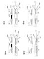
- FIG. 3 is a diagram showing a relationship between a primary side non-contact charging module including a magnet and a charging coil according to the embodiment of the present invention.
- 3A shows a case where a positioning magnet is used when the inner width of the charging coil is small
- FIG. 3B shows a case where a positioning magnet is used when the inner width of the charging coil is large
- FIG. 3C shows an inner width of the charging coil
- 3D shows a case where the alignment magnet is not used when the inner width of the charging coil is large.
- the primary side non-contact charging module 200 disposed in the charger includes a primary side coil 210, a magnet 220, and a magnetic sheet (not shown).
- FIG. 3 schematically shows the magnetic sheet 10, the charging coil 30, and the NFC coil 40 in the non-contact charging module 100.
- the contactless charging module 100 and the primary side contactless charging module 200 are aligned so that the primary side coil 210 and the charging coil 30 face each other.
- a magnetic field is also generated between the inner portion 211 of the primary coil 210 and the inner portion 33 of the charging coil 30 to transmit power.
- the inner part 211 and the inner part 33 are opposed to each other. Further, the inner portion 211 and the inner portion 33 are also portions close to the magnet 220, and are easily affected by the magnet 220.
- the magnet 220 when the magnet 220 is disposed in the vicinity of the magnetic sheet 10 and the magnetic body 20, the magnetic permeability of the magnetic sheet 10 in the vicinity of the magnet 220 is lowered.
- the magnetic sheet 10 is closer to the magnet 220 than the magnetic body 20 and is easily affected by the magnet 220. Therefore, the magnet 220 provided in the primary side non-contact charging module 200 weakens the magnetic fluxes of the primary side coil 210 and the charging coil 30, particularly the inner portion 211 and the inner portion 33, and has an adverse effect. As a result, the transmission efficiency of non-contact charging is reduced. Therefore, in the case of FIG. 3A, the inner portion 33 that is easily affected by the magnet 220 becomes larger.
- the L value increases because the number of turns of the charging coil 30 is large.
- the numerical value is greatly reduced from the L value in FIG. 3C to the L value in FIG. 3A, in the case of the coil having a small inner width, the magnet 220 is provided for alignment and the case where it is provided.
- the value reduction rate becomes very large.
- the inner width of the charging coil 30 is smaller than the diameter of the magnet 220, the charging coil 30 is directly affected by the magnet 220 by an area facing the magnet 220. Therefore, the inner width of the charging coil 30 is preferably larger than the diameter of the magnet 220.
- the inner width of the charging coil 30 is large as shown in FIG. 3B, the inner portion 33 that is easily affected by the magnet 220 becomes very small. 3D in which the magnet 220 is not used, the L value is smaller than that in FIG. 3C because the number of turns of the charging coil 30 is reduced. As a result, since the decrease in the numerical value is small from the L value in FIG. 3D to the L value in FIG. 3B, the L value reduction rate can be kept small in a coil having a large inner width. Moreover, since the edge part of the hollow part of the charging coil 30 leaves
- the charging coil 30 cannot be formed in a certain size or more. Accordingly, if the inner width of the charging coil 30 is increased to reduce the adverse effect from the magnet 220, the number of turns decreases, and the L value itself decreases regardless of the presence or absence of the magnet 220. Therefore, the area of the magnet 220 and the area of the hollow portion of the charging coil 30 are substantially the same (the outer diameter of the magnet 220 is smaller by about 0 to 2 mm than the inner width of the charging coil 30, or the area of the magnet 220 is that of the charging coil 30.
- the magnet 220 can be maximized, so the alignment accuracy between the primary side non-contact charging module and the secondary side non-contact charging module Can be improved.
- the area of the magnet 220 is smaller than the area of the hollow portion of the charging coil 30 (the outer diameter of the magnet 220 is about 2 to 8 mm smaller than the inner width of the charging coil 30, or the area of the magnet 220 is hollow of the charging coil 30. (About 45% to 75% of the area of the portion), the magnet 220 can be made not to exist between the portions where the inner portion 211 and the inner portion 33 face each other even if the alignment accuracy varies.
- the influence of the magnet 220 can be suppressed when wound in a substantially rectangular shape rather than being wound in a circular shape. . That is, a comparison is made between a circular coil whose hollow portion has a diameter x and a substantially square coil whose distance between opposite sides (length of one side) of the hollow portion is x. At this time, when conducting wires having the same wire diameter are wound with the same number of turns, they are accommodated between the non-contact charging modules 100 having the same width. At this time, the diagonal length y of the hollow portion of the substantially square coil is y> x.
- the diameter of the magnet 220 is m
- the distance between the innermost end of the circular coil and the magnet 220 is always (x ⁇ m) constant (x> m).
- the minimum distance between the innermost end portion of the substantially rectangular coil and the magnet 220 is (x ⁇ m)
- the maximum is (ym) in the corner portions 31a to 31d.
- the size can be further reduced. That is, even if the short side of the hollow portion that is substantially rectangular is smaller than m, the four corner portions can be arranged outside the outer periphery of the magnet 220 if the long side is larger than m. Therefore, when the charging coil 30 is wound in a substantially rectangular shape around the substantially rectangular hollow portion, at least the long side of the hollow portion only needs to be larger than m.
- the innermost end of the charging coil 30 is outside the magnet 220 provided in the primary-side non-contact charging module 200, or the four corners of the substantially rectangular hollow portion of the charging coil 30 wound in a substantially rectangular shape. Being outside the magnet 220 means something like FIG. 3B. That is, when the end of the circular surface of the magnet 220 is extended in the stacking direction and extended to the non-contact charging module 100, the region surrounded by the extension line fits in the hollow portion of the charging coil 30.
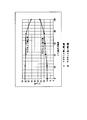
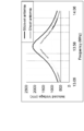
- FIG. 4 shows the relationship between the charging coil inner diameter and the charging coil L value when the outer diameter of the charging coil is constant when the primary non-contact charging module is provided with a magnet and when the magnet is not provided.
- FIG. 4 shows the relationship between the charging coil inner diameter and the charging coil L value when the outer diameter of the charging coil is constant when the primary non-contact charging module is provided with a magnet and when the magnet is not provided.
- FIG. 4 shows the relationship between the charging coil inner diameter and the charging coil L value when the outer diameter of the charging coil is constant when the primary non-contact charging module is provided with a magnet and when the magnet is not provided.
- FIG. 4 shows the relationship between the charging coil inner diameter and the charging coil L value when the outer diameter of the charging coil is constant when the primary non-contact charging module is provided with a magnet and when the magnet is not provided.
- FIG. 4 shows the relationship between the charging coil inner diameter and the charging coil L value when the outer diameter of the charging coil is constant when the primary non-contact charging module is provided with a magnet and when the magnet
- the outer diameter of the coil is unified to 30 mm.
- the distance between the end of the hollow portion of the charging coil 30 (the innermost end of the charging coil 30) and the outer end of the magnet 220 is greater than 0 mm and smaller than 6 mm, so that the L value is 15 ⁇ H or more.
- the L value between when the magnet 220 is used and when it is not used can be made closer.
- the conducting wire of the charging coil 30 may be formed by laminating one conducting wire in a plurality of stages, and this laminating direction is the same as the laminating direction in which the magnetic sheet 10 and the charging coil 30 are laminated.
- the layers of the conductive wires arranged vertically are stacked so as to leave a space between each other, so that the stray capacitance between the upper conductive wire and the lower conductive wire is reduced, and the AC resistance of the charging coil 30 is reduced. be able to.
- the thickness of the charging coil 30 can be suppressed by being wound so as to close the space.
- corner portions (corners) 31a to 31d are provided as follows.
- the charging coil 30 wound in a substantially square shape is one in which the corners 31a to 31d at the corners 31a to 31d of the hollow portion have R (the radius of the curve at the four corners) of 30% or less of the side width of the hollow portion. That is, in FIG. 2B, the substantially square hollow portion has curved corners.
- the strength of the conducting wire at the four corners can be improved by being slightly curved rather than perpendicular. However, if R becomes too large, there is almost no change from the circular coil, and the effect unique to the substantially square charging coil 30 cannot be obtained.
- the side width of the hollow portion is 20 mm, for example, if the radius R of the curve at each corner is 6 mm or less, the influence of the magnet 220 can be more effectively suppressed.
- the effect of the most rectangular coil described above can be obtained because the radius R of the curve at each corner is 5 to 30% of the side width of the hollow portion of the substantially square shape. it can.
- the radius R of the curve at each of the four corners is 5 to 30% of the side width (either the short side or the long side) of the hollow portion of the substantially rectangular shape.
- the corners of the four corners of the innermost end (hollow part) of the charging coil 30 have R of 2 mm, preferably about 0.5 mm to 4 mm.
- the leg portions 32a and 32b are preferably provided in the vicinity of the corner portions 31a to 31d.
- the leg portions 32a and 32b can be provided at portions where the planar coil portion is wound in a curved line.
- the force with which the coil tries to maintain the shape of the coil itself differs between the side portion (straight portion) and the corner portion. That is, a large force for maintaining the shape of the charging coil 30 acts at the corner portions 31a to 31d in FIG. 2B.
- the force for maintaining the shape of the charging coil 30 is small at the side portion, and the conductive wire can be easily unwound from the charging coil 30 around the curves of the corner portions 31a to 31d.
- the number of turns of the charging coil 30 varies by, for example, about 1/8 turn, and the L value of the charging coil 30 varies.
- the conducting wire bends the corner portion 31a immediately after the winding start point on the leg portion 32a side is close to the corner portion 31a.
- the winding start point and the corner portion 31a may be adjacent to each other. And it winds several times and becomes a point of the end of winding just before turning the corner part 31a, and a conducting wire becomes the leg part 32b and is bent to the outer side of the charging coil 30. At this time, the bending of the conducting wire bends more slowly at the winding end point than at the winding start point. This is to improve the force for maintaining the shape of the leg portion 32b.
- the lead wire is a litz wire
- the force for maintaining the shape of the charging coil 30 is further improved. Since the litz wire has a large surface area, it is easy to fix the shape of the charging coil 30 with an adhesive or the like.
- the conducting wire is a single wire, since the surface area per conducting wire is small, the surface area to be bonded is small, and the shape of the charging coil 30 is easy to unwind.
- the charging coil 30 is formed using a conducting wire having a circular cross-sectional shape, but the conducting wire used may be a conducting wire having a square cross-sectional shape.
- the conducting wire used may be a conducting wire having a square cross-sectional shape.
- the magnetic sheet 10 includes a flat portion 12 on which the charging coil 30 is placed, a central portion 13 that is substantially in the center of the flat portion 12 and that corresponds to (opposes) the hollow region of the charging coil 30, and the charging coil 30.
- the slit 11 into which at least a part of the two leg portions 32a and 32b is inserted.
- the slit 11 may not be formed as shown in FIG. 1, and may be not only a slit shape penetrating but also a recess shape not penetrating as shown in FIG. 2.
- the central portion 13 has a convex shape, a flat shape, a concave shape, or a shape that is a through hole with respect to the flat portion 12, and may be any shape. If it is a convex shape, the magnetic flux of the charging coil 30 can be strengthened. If it is flat, it is easy to manufacture and easy to place the charging coil 30, and it is possible to balance the influence of an alignment magnet 220 described later and the L value of the charging coil 30.
- the concave shape and the through hole will be described in detail later.
- the magnetic sheet 10 a Ni—Zn based ferrite sheet (sintered body), a Mn—Zn based ferrite sheet (sintered body), a Mg—Zn based ferrite sheet (sintered body), or the like may be used. It can. A single-layer configuration may be used, a configuration in which a plurality of the same materials are stacked in the thickness direction, or a plurality of different magnetic sheets 10 may be stacked in the thickness direction. It is preferable that at least the magnetic permeability is 250 or more and the saturation magnetic flux density is 350 mT or more.
- An amorphous metal can also be used as the magnetic sheet 10.
- a ferrite sheet is used as the magnetic sheet 10
- the charging coil 30 can be made thin.
- the magnetic sheet 10 is substantially square and has a size of about 40 ⁇ 40 mm (35 mm to 50 mm). In the case of a substantially rectangular shape, the size is 35 mm (25 mm to 45 mm) on the short side and 45 mm (35 mm to 55 mm) on the long side. The thickness is 0.43 mm (actually between 0.4 mm and 0.55 mm and may be about 0.3 mm to 0.7 mm).
- the magnetic sheet 10 is desirably formed to be approximately the same or larger than the outer peripheral end of the magnetic body 20.
- the shape of the magnetic sheet 10 may be a circle, a rectangle, a polygon, a rectangle having a large curve at four corners, and a polygon.
- the slit 11 accommodates the conductive wire of the leg portion 32 a from the winding start point 32 aa (the innermost part of the coil) of the charging coil 30 to the lower end portion of the magnetic sheet 10. This prevents the conductive wire from the winding start point 32aa to the leg portion 32a of the charging coil 30 from overlapping the planar winding portion of the charging coil 30 in the stacking direction.
- the slit 11 is formed so as to be substantially perpendicular to the end portion (end side) of the magnetic sheet 10 at which one end thereof intersects and to contact the central portion 13 of the magnetic sheet 10.
- the leg portions 32a and 32b can be formed without bending the winding start point 32aa of the conducting wire by forming the slit 11 so as to overlap the tangent of the central portion 13 (circular).
- the legs 11a and 32b are formed without bending the winding start of the conducting wire by forming the slit 11 so as to overlap the extended line of the side of the central portion 13 (substantially rectangular). can do.
- the length of the slit 11 depends on the inner diameter of the charging coil 30 and the size of the magnetic sheet 10, and is about 15 mm to 30 mm in the present embodiment.
- the slit 11 may be formed at a portion where the end portion (end side) and the center portion 13 of the magnetic sheet 10 are closest to each other. That is, when the charging coil 30 is circular, the slit 11 is perpendicular to the tangent line of the end (end) of the magnetic sheet 10 and the center 13 (circular), and the slit 11 is formed short. Moreover, when the charging coil 30 is substantially rectangular, the slit 11 is formed to be short with respect to the end portion (end side) of the magnetic sheet 10 and the side of the center portion 13 (substantially rectangular shape). Thereby, the formation area of the slit 11 can be suppressed to the minimum, and the transmission efficiency of the non-contact power transmission device can be improved. In this case, the length of the slit 11 is about 5 mm to 20 mm. In either arrangement, the inner end of the slit 11 (slit) is connected to the central portion 13.
- the magnetic sheet 10 has a lower magnetic permeability particularly in the portion near the magnet 220 due to the influence of the magnet 220. Accordingly, the L value of the charging coil 30 varies greatly depending on whether or not the primary-side non-contact charging module 200 includes the magnet 220 for alignment. Therefore, it is necessary to make the magnetic sheet 10 the L value of the charging coil 30 that does not change as much as possible when the magnet 220 approaches or does not approach.
- the electronic device to be mounted is a mobile phone
- it is often arranged between the case constituting the exterior of the mobile phone and the battery pack located in the case, or on the case and the board located in the case.
- a battery pack is an aluminum casing, it adversely affects power transmission. This is because an eddy current is generated in aluminum in a direction in which the magnetic flux generated by the coil is weakened, so that the magnetic flux of the coil is weakened. Therefore, it is necessary to provide the magnetic sheet 10 between the aluminum that is the exterior of the battery pack and the charging coil 30 disposed on the exterior of the battery pack to reduce the influence on the aluminum.
- the electronic components mounted on the board may interfere with the power transmission of the charging coil 30 and adversely affect each other. Therefore, it is necessary to provide the magnetic sheet 10 or a metal film between the substrate and the charging coil 30 to suppress the mutual influence.
- the magnetic sheet 10 used in the non-contact charging module 100 is used with a high magnetic permeability and saturation magnetic flux density, and it is important to increase the L value of the charging coil 30 as much as possible.
- Any material having a magnetic permeability of 250 or more and a saturation magnetic flux density of 350 mT or more may be used.
- the sintered body of Mn—Zn ferrite has a magnetic permeability of 1500 to 2500, a saturation magnetic flux density of 400 to 500, and a thickness of about 400 ⁇ m to 700 ⁇ m.
- Ni—Zn ferrite may be used, and if the magnetic permeability is 250 or more and the saturation magnetic flux density is 350 or more, good power transmission with the primary side non-contact charging module 200 is possible.
- the charging coil 30 forms an LC resonance circuit using a resonance capacitor.
- the resonance frequency with the resonance capacitor also greatly increases. Will change. Since this resonance frequency is used for power transmission (charging) between the primary-side non-contact charging module 200 and the non-contact charging module 100, if the resonance frequency changes greatly depending on the presence or absence of the magnet 220, power transmission cannot be performed correctly. End up.
- variation in the resonance frequency due to the presence or absence of the magnet 220 is suppressed, and power transmission is highly efficient in any situation.
- the magnetic sheet 10 is a ferrite sheet and is based on Mn—Zn, it is possible to further reduce the thickness. That is, according to the standard (WPC), the frequency of electromagnetic induction is determined to be about 100 kHz to 200 kHz (for example, 120 kHz). In such a low frequency band, the Mn—Zn ferrite sheet has high efficiency. Note that the Ni—Zn ferrite sheet is highly efficient at high frequencies. Therefore, in this embodiment, the magnetic sheet 10 for non-contact charging that transmits power at about 100 kHz to 200 kHz is composed of a Mn—Zn ferrite sheet, and the magnetic sheet for NFC communication that performs communication at about 13.56 MHz.
- the body 20 is composed of a Ni—Zn ferrite sheet. As described above, by configuring the magnetic sheet 10 and the magnetic body 20 with different types of ferrite, each can efficiently perform communication and power transmission. Moreover, even if the magnetic sheet 10 and the magnetic body 20 are made thinner and smaller, sufficient efficiency can be obtained.
- a hole may be formed in the central portion 13 of the magnetic sheet 10.
- any of a through-hole and a recessed part may be sufficient as a hole.
- a hole may be larger than the center part 13 and may be small, the smaller one is good. That is, when the charging coil 30 is placed on the magnetic sheet 10, the charging coil 30 may be larger or smaller than the hollow portion of the charging coil 30. When it is small, the entire charging coil 30 is placed on the magnetic sheet 10.
- the contactless charging module 100 can be adapted to both the primary side (charging side) contactless charging module using a magnet and the primary side contactless charging module 200 not using a magnet.
- charging is possible regardless of the type of the primary side non-contact charging module 200, and convenience is improved.
- the L value of the charging coil 30 when the primary non-contact charging module 200 is provided with the magnet 220 and the L value of the charging coil 30 when the magnet 220 is not provided are brought close to each other, and both L values are improved. Desired.
- the magnet 220 is disposed in the vicinity of the magnetic sheet 10
- the magnetic permeability of the central portion 13 of the magnetic sheet 10 in the vicinity of the magnet 220 is lowered. Therefore, by providing a hole in the central portion 13, it is possible to suppress a decrease in magnetic permeability.
- FIG. 5 is a diagram showing the relationship between the L value of the charging coil and the hollowing ratio of the central portion when the primary non-contact charging module is provided with a magnet and when it is not provided.
- the percentage of hollowing out means 100% means that the hole in the central portion 13 is a through hole, and the percentage of hollowing out means that no hole is provided.
- the percentage cut out means 50% means that a hole (concave portion) having a depth of 0.3 mm is provided on a magnetic sheet having a thickness of 0.6 mm, for example.
- the L value decreases as the cut-out ratio is increased when the magnet 220 is not provided in the primary-side non-contact charging module 200.
- the hollowing out ratio hardly decreases from 0% to 75%, but greatly decreases from 75% to 100%.
- the L value is improved as the hollowing ratio is increased. This is because it is less likely to be adversely affected by the magnet.
- the L value is gradually improved when the cut-out ratio is from 0% to 75%, and is greatly improved from 75% to 100%.
- the primary side non-contact charging module 200 has the magnet 220 while maintaining the L value when the primary side non-contact charging module 200 is not provided with the magnet 220. Can be improved. Further, when the cut-out ratio is 75% to 100%, the L value when the magnet 220 is not provided in the primary-side non-contact charging module 200 and the case where the magnet 220 is provided in the primary-side non-contact charging module 200. The L value can be made much closer. It is most effective when the cut-out ratio is 40 to 60%, and the primary side non-contact is maintained while maintaining the L value when the magnet 220 is not provided in the primary side non-contact charging module 200. When the magnet 220 is provided in the charging module 200, the L value is improved by 1 ⁇ H or more, and when the magnet 220 is further provided, the magnet 220 and the magnetic sheet can sufficiently attract each other.
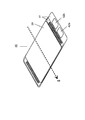
- FIG. 6 is a perspective view when the NFC coil and the magnetic body in the present embodiment are assembled.
- FIG. 7 is an exploded view showing the arrangement of the NFC coil and the magnetic body in the present embodiment.
- the NFC coil 40 in the present embodiment shown in FIG. 6 is an antenna that performs short-range wireless communication that performs communication by electromagnetic induction using a frequency of 13.56 MHz band, and a sheet antenna is generally used.
- the NFC coil 40 of this embodiment is a coil pattern that is arranged so as to wrap around the magnetic body 20 formed of ferrite or the like, and is formed on a support mainly made of resin.
- a flexible substrate 41 is provided as a conductor arrangement portion.
- the NFC coil 40 generates magnetic field lines for NFC communication for communicating with a wireless communication medium such as an IC card or an IC tag (not shown).
- a wireless communication medium such as an IC card or an IC tag (not shown).
- 6 and 7 the specific shape of the coil pattern is not shown, but a coil pattern having a straight line S having an arrow as a coil axis is formed.
- the coil pattern and the adjustment pattern which will be described later, are usually formed by a copper foil formed between two resin layers of the flexible substrate 41, such as a polyimide film and a coverlay or a resist.
- the flexible substrate 41 is divided into two parts with the magnetic body 20 in between.
- the side having the external connection terminals 42a, 42b is defined as the lower flexible substrate (first arrangement portion) 41a, and the other side is defined as the upper flexible substrate.
- a substrate (second arrangement portion) 41b is assumed.
- the lower flexible board 41a and the upper flexible board 41b are joined by solder.
- the flexible substrate 41 is joined at two sides substantially parallel to the coil axis S.
- the “lower side” and “upper side” here are given for convenience in order to facilitate understanding in FIG. 7, and may be turned upside down when mounted on the device as the NFC coil 40. .
- the width of the upper flexible board 41b in the coil axis S direction is set so that the magnetic body 20 does not protrude. This is because, particularly when the magnetic body 20 is made of a ferrite that is easily broken, the fragments and residues are scattered in the communication device (for example, the portable terminal 1 in FIG. 1) in which the NFC coil 40 is incorporated, which adversely affects the communication device. This is to avoid giving them.
- the size of the magnetic body 20 is 5 mm ⁇ 36 mm ⁇ 0.21 mm.
- the width in the longitudinal direction is preferably 25 mm to 50 mm. As shown in FIG. 1, it is preferable to form the magnetic sheet 10 to be larger than the width in the same direction. As a result, in NFC communication, there are portions (both ends) that are not easily affected by the charging coil 30 (hard to be coupled), so the efficiency of NFC communication can be improved.
- the width in the short direction may be about 3 to 10 mm. It depends on the number of turns of the NFC coil 40.
- the thickness is preferably smaller than the thickness when the magnetic sheet 10 and the charging coil 30 are laminated, and is preferably about 0.15 to 1 mm.
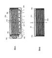
- FIG. 8 is a diagram showing the wiring of the NFC coil in the present embodiment.
- 8A is a view of the lower flexible substrate 41a as viewed from the contact surface with the magnetic body 20
- FIG. 8B is a view of any of the upper flexible substrate 41b as viewed from the contact surface with the magnetic body 20.
- the arrow direction of the coil axis S is the front side in the perspective view of the flexible substrate 41 shown in FIGS.
- the lower flexible substrate 41a has external connection terminals 42a and 42b in addition to the division pattern 43a.
- these copper foils are also so-called “exposed” and soldered. A plating process is performed.
- a plurality of divided patterns 43a that are part of the NFC coil 40 are formed so as to be parallel to each other and intersect the coil axis S.
- a plurality of divided patterns 43b, which are also part of the coil pattern, are formed on the upper flexible substrate 41b so as to be parallel to each other and intersect the coil axis S.
- the copper foil is "exposed" at both ends of the plurality of divided patterns 43a and 43b by the pattern exposed portions 44a and 44b and the pattern exposed portions 45a and 45b, respectively.
- the conductor pattern starting from the external connection terminal 42a on the lower flexible substrate 41a by repeating the solder bonding of the plurality of conductor patterns 43a and 43b divided across the magnetic body 20 as described above, After going around the magnetic body 20, it is connected to the external connection terminal 42b.
- a helical conductor pattern is formed around the coil axis S of the magnetic body 20.
- This spiral conductor pattern is a so-called coil pattern, and can generate magnetic lines of force for communicating with a wireless communication medium such as an IC card or an IC tag.
- the conductor pattern formed on the flexible substrate 41 of this embodiment is not limited to the spiral coil pattern.
- FIG. 8A there is provided an adjustment pattern u which will be described in more detail, connected to the division pattern t located on one side of the outermost edge.
- the adjustment pattern u has a plurality of lead patterns v in which the divided pattern t and one end are connected. Further, the other end portions of the drawing patterns v not connected to the divided pattern t and the protruding side end portions (dotted lines) of the protruding portion drawing pattern z constituting a part of the protruding portion y of the divided pattern t. And an end portion located outside the outer shape of the magnetic body 20 shown in FIG.
- the adjustment pattern u is provided only on the lower flexible substrate 41a side.
- the plurality of divided patterns 43a and 43b forming the coil pattern shown in FIGS. 8A and 8B are divided and provided on both the lower flexible substrate 41a and the upper flexible substrate 41b.
- the lower flexible board 41a is provided with external connection terminals 42a and 42b in addition to the adjustment pattern u, and has a larger outer shape than the upper flexible board 41b.
- a part of these adjustment patterns u that is, all of the connection patterns w and a part of the lead pattern v), a part of the protruding portion y of the divided pattern t, and the external connection terminals 42a and 42b are dotted lines.
- the antenna device can be configured by connecting to the electronic circuit board disposed on the surface.
- the adjustment pattern not covered by the magnetic body 20 and the upper flexible substrate 41b has at least a connection pattern w.
- the NFC shown in FIG. When the assembly of the coil 40 is completed, the inductance can be adjusted.
- the inductance of the NFC coil 40 is one factor that determines the resonance frequency of the antenna device when the NFC coil 40 in FIG. 1 is connected to an electronic circuit board on which a matching circuit and other antenna control units are mounted to form an antenna device. Is.
- the inductance of the NFC coil 40 having the structure of the present embodiment is greatly influenced by the size variation of the magnetic body 20. This is because the apparent permeability is different when the size of the magnetic body 20 is different.
- the resonance frequency of the antenna device equipped with the NFC coil 40 also varies.
- the resonance frequency of the antenna device equipped with the NFC coil 40 By adjusting the resonance frequency within a predetermined range from the center frequency (for example, 13.56 MHz for RF-ID) defined in the communication standard, wireless communication can be performed with high probability and quality.
- the variation in inductance of the NFC coil 40 alone is reduced (for example, within ⁇ 2%)
- the adjustment range necessary for adjusting the resonance frequency of the antenna device on which the NFC coil 40 is mounted is reduced. can do. Therefore, the line length of the coil pattern is adjusted to suppress the inductance variation of the NFC coil 40 due to the size variation of the magnetic body 20.
- Trimming of the coil pattern for adjusting the inductance of the NFC coil 40 is performed at a portion outside the outer shape of the magnetic body 20 indicated by a dotted line in the lead pattern v or the protruding portion lead pattern z in FIG. Since these portions are not covered with the magnetic body 20 and the upper flexible substrate 41, the trimming operation can be easily performed.
- the difference in the number of turns of the coil pattern wound around is c.
- the protrusion lead-out pattern z constituting a part of the protrusion y also contributes to the adjustment of the inductance of the coil pattern. Since the divided pattern t constituting the coil pattern has the protruding portion y positioned outside the outer shape of the magnetic body 20, even if the NFC coil 40 shown in FIG. A sufficient margin can be secured. 8 is a part that contributes to the adjustment of the inductance of the coil pattern together with the adjustment pattern u, and therefore must be provided on the flexible substrate on the same side as the adjustment pattern u.
- FIG. 9 is a conceptual diagram showing an antenna device formed by an electronic circuit board and an NFC coil mounted on the portable terminal in the present embodiment, and magnetic lines generated from the antenna device.
- the antenna device in the present embodiment includes a magnetic body 20, an NFC coil 40, and an electronic circuit board disposed in the vicinity of the NFC coil 40.
- a wiring pattern for connecting terminals of circuit components mounted thereon is provided on the surface or inside of the electronic circuit board.
- the power supply line and the GND (ground) line supplied to each circuit component are often provided as a wiring layer different from the wiring pattern described above.
- these wiring patterns, power supply lines, and GND lines are conductors such as copper. That is, the electronic circuit board (metal body 50) can be regarded as a metal body. As described above, when the power supply line and the GND line are provided as separate wiring layers, these are formed over almost the entire surface of the assigned wiring layer, so that a particularly high-quality metal body is obtained.
- the opening of the coil part of the NFC coil 40 is perpendicular to the electronic circuit board.
- 40 is disposed at the end of the electronic circuit board.
- the end of the electronic circuit board refers to the case where the end of the NFC coil 40 protrudes from the outermost end of the electronic circuit board, and the end of the NFC coil 40 than the outermost end of the electronic circuit board. Including both cases of being located inside.
- the NFC coil 40 is arranged so that the opening of the NFC coil 40 is perpendicular to the electronic circuit board and the longitudinal direction of the NFC coil 40 is substantially parallel to the endmost part of the electronic circuit board (NFC coil 40 Are arranged along the extreme end of the electronic circuit board). Thereby, for example, even if the non-contact type IC card is positioned not only in the area P but also in the area Q, good communication can be performed.
- the opening of the NFC coil 40 is perpendicular to the electronic circuit board, when a signal is input to the NFC coil 40 and a current flows, all the lines of magnetic force M generated from the NFC coil 40 are generated from the NFC coil 40 in the region Q.
- the magnetic field lines M pass only in one direction.
- a current flows through, for example, the non-contact type IC card located in the region Q, and the portable terminal equipped with the antenna device of this embodiment including the electronic circuit board and the NFC coil 40 communicates with the non-contact type IC card. It can be performed.
- the magnetic field lines M are either in the direction away from the NFC coil 40 or in the direction toward the NFC coil 40. This is because the magnetic force lines M generated from the NFC coil 40 are attenuated near the electronic circuit board, so that the axis C of the magnetic force lines M is not perpendicular to the electronic circuit board and is inclined.
- a current flows through, for example, a non-contact type IC card located in the region P, and the portable terminal equipped with the antenna device of the present embodiment including the electronic circuit board and the NFC coil 40 communicates with the non-contact type IC card. It can be performed.
- the magnetic field lines M shown in FIG. 9 have an axis C that connects the boundary between the magnetic field lines in the direction away from the NFC coil 40 and the magnetic field lines in the direction toward the NFC coil 40.
- a non-contact type IC card is positioned in the vicinity of the axis C of the magnetic force lines M, both the magnetic lines in the direction away from the antenna and the direction toward the antenna act on the non-contact type IC card and cancel each other. As a result, no current flows through the non-contact type IC card, and communication between the portable terminal equipped with the antenna device of this embodiment and the non-contact type IC card is not performed.
- the NFC coil 40 is arranged at the end of the electronic circuit board, the magnetic field lines M on the electronic circuit board side (right side in FIG. 6) of the NFC coil 40 are attenuated and the NFC coil 40 is away from the electronic circuit board ( The magnetic field lines M on the left side in FIG. 6 are relatively strengthened. As a result, the axis C of the magnetic force line M is inclined with respect to the electronic circuit board. In the configuration of this embodiment, the angle ⁇ of the axis C of the magnetic lines of force M is inclined to be about 40 ° to 85 ° with respect to the electronic circuit board.
- the NFC coil 40 is not disposed at the end of the electronic circuit board, the magnetic field lines in the direction perpendicular to the electronic circuit board surface due to the eddy current on the electronic circuit board surface are reduced, and the axis C of the magnetic force lines M is the electronic circuit board. Remains almost perpendicular to. In that case, even if communication is possible in region Q, communication cannot be performed in region P.
- the end of the NFC coil 40 and the electronic circuit board may be arranged with their ends aligned, or the end of the NFC coil 40 may protrude beyond the end of the electronic circuit board. Further, the end portion of the NFC coil 40 may be located inside the end portion of the electronic circuit board.
- the NFC coil 40 at the end of the electronic circuit board, the current flowing through the electronic circuit board can be fully utilized. Further, if the angle ⁇ is about 85 °, the effect of the present invention can be obtained, and preferably 80 ° or less.
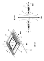
- FIG. 10 is a schematic diagram of lines of magnetic force generated by the charging coil and the NFC coil in the present embodiment.
- the opening of the NFC coil 40 in the present embodiment is perpendicular to the metal body 50 and is arranged at the end of the metal body 50.
- the distance between the outer end of the NFC coil 40 and the outermost end of the metal body 50 is about ⁇ 5 mm to +5 mm.
- d is a negative value means that the outer end portion of the NFC coil 40 is located on the inner side of the outermost end portion of the metal body 50, and in this case, it is 2 cm inside. Indicates. Conversely, if d is a positive value, it indicates that the outer end portion of the NFC coil 40 protrudes outward from the outermost end portion of the metal body 50.
- ⁇ 5 mm to +5 mm is caused by the width of the magnetic body 20 in the short direction. That is, assuming that the width of the magnetic body 20 in the short direction is d, the distance between the outer end portion of the NFC coil 40 and the outermost end portion of the metal body 50 is about ⁇ dmm to + dmm. Thereby, the NFC communication as described above can be performed satisfactorily.
- the opening surface is directed in the same direction. This is because both of them are coiled in a plane, and in order to improve communication efficiency and charging efficiency, it is necessary to enlarge the respective openings, so that electronic devices that are required to be smaller and thinner This is because the above-mentioned configuration is inevitably obtained. That is, since both the non-contact charging module and the NFC sheet antenna mounted on the miniaturized electronic device casing are communication (power transmission) using electromagnetic induction, the charging coil and the opening surface of the NFC sheet antenna This is because the L value is improved by increasing.
- the NFC sheet antenna takes away the magnetic flux for power transmission between the contactless charging module of the charger for contactless charging and the charging coil on the charged side. Furthermore, the NFC sheet antenna also receives magnetic flux generated when the charging coil receives power. Therefore, the power transmission efficiency of the NFC sheet antenna is reduced, and the charging time is increased. Also, when short-range communication is performed using the NFC sheet antenna, an eddy current is generated in the charging coil in the direction of weakening the magnetic flux generated by the NFC sheet antenna.
- the charging coil for flowing a large current has a larger conductor thickness than an NFC sheet antenna that performs communication by flowing a small current. Therefore, when viewed from the NFC sheet antenna, the charging coil becomes a huge metal, and when viewed from the NFC sheet antenna, the eddy current generated in the charging coil cannot be ignored. Therefore, it has an adverse effect on the short-range communication efficiency and communication distance of the NFC sheet antenna.
- the charging coil and the NFC sheet antenna are completely stacked centered on each other, there will be two large planar coils on the surface of the housing, and whichever is covered when viewed from the non-contact charging module on the charger side. It is difficult to determine whether the charging coil is for charging. When the alignment accuracy is lowered, the power transmission efficiency is lowered accordingly.
- the non-contact charger detects the position of the charging coil to automatically move the planar coil of the non-contact charger (primary side) to the position of the charging coil.
- the detection method such as using the resonance frequency of the charging coil, but there is a possibility that the resonance frequency of the NFC sheet antenna is detected and aligned with the NFC sheet antenna.
- a mobile terminal device can be charged anywhere on the charging surface of the non-contact charger (primary side) by arranging a large number of coils on the non-contact charger (primary side).
- the coil (primary side) close to the NFC sheet antenna transmits a large amount of magnetic flux that is not necessary for the NFC sheet antenna. As a result, there is a risk of wasteful power consumption or malfunction.
- the magnet provided in the non-contact charger may be attracted to the magnet provided in the hollow portion of the magnetic sheet or the charging coil for alignment.
- the magnetic sheet for the NFC sheet antenna since the magnetic sheet for the NFC sheet antenna is saturated by the magnet and the magnetic permeability may be lowered, the L value of the NFC sheet antenna may be lowered. In that case, the communication distance and communication efficiency of the NFC sheet antenna may be reduced.
- the NFC sheet antenna faces the opening surface in substantially the same direction as the charging coil and generates magnetic flux in substantially the same direction. Therefore, regardless of the alignment method, the communication performance of the NFC sheet antenna and the charging coil The power transmission performance is adversely affected.
- the coil axis A of the charging coil 30 is in the vertical direction in the figure.
- the coil axis B of the NFC coil 40 is in the left-right direction in the drawing.
- they are in a substantially vertical relationship with each other.
- the charging coil 30 and the NFC coil 40 can communicate in substantially the same direction. This is because the NFC coil 40 behaves as described in FIG.
- the NFC coils 40 may be wound so that the magnetic fluxes of all the NFC coils 40 extend in the same direction (for example, upward in FIG. 10B). That is, both of the two NFC coils 40 in FIG. 10A are wound clockwise as viewed from the outside.
- the NFC coil 40 is preferably arranged on the outer side of the charging coil 30 because it is preferable to be arranged on the end side rather than the center side of the metal body 50. As shown in FIG. 10, it is not always necessary to arrange the charging coil 30 around the charging coil 30. However, since the axis C of the magnetic flux is inclined by the metal body 50, the charging coil 30 is preferably arranged on both sides. In FIG. 10, two NFC coils 40 are connected in a loop shape so as to surround the charging coil 30.
- the non-contact charging module 100 can be reduced in size. If the width in the longitudinal direction of the NFC coil 40 is substantially the same as the width in the same direction of the charging coil 30, the contactless charging module 100 can be reduced in size. Further, in order to sufficiently tilt the magnetic flux axis C of the NFC coil 40, it is preferable that the magnetic sheet 10 is not disposed under the NFC coil 40.
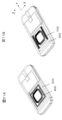
- FIG. 11 is a perspective view showing a portable terminal including a contactless charging module according to the present embodiment and a contactless charging module including a loop-shaped NFC coil for comparison.
- FIG. 12 is a diagram illustrating frequency characteristics of induced voltages of the two contactless charging modules illustrated in FIG. 11.
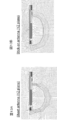
- FIG. 13 is a diagram showing the magnetic field in the YZ plane of each of the two contactless charging modules shown in FIG.
- FIG. 14 is a diagram illustrating the magnetic field in the ZX plane of each of the two contactless charging modules illustrated in FIG. 11.
- 11A, FIG. 13A, and FIG. 14A show the case of a non-contact charging module provided with a loop-shaped NFC antenna for comparison
- FIGS. 11B, 13B, and 14B show the non-contact charging module in the embodiment. This case is shown.
- the non-contact charging module 100 and the non-contact charging module 400 provided with a loop-shaped NFC antenna in the present embodiment are placed on the battery pack 303 so as to be stacked.
- the power transmission direction of the charging coil 30 and the communication direction of the NFC coil 40 of the contactless charging modules 100 and 400 are the back surface of the portable terminal (the surface on which a display unit such as a liquid crystal screen is disposed is the front surface).
- the induced electromotive force of the NFC coil 40 of the non-contact charging module 100 is larger than the induced electromotive force of the loop-shaped NFC coil of the non-contact charging module 400.
- the NFC coil 40 of the contactless charging module 100 has higher communication efficiency than the loop-shaped NFC coil of the contactless charging module 400.
- the NFC coil 40 of the non-contact charging module 100 has a wider communication area than the loop-shaped NFC coil of the non-contact charging module 400.
- the non-contact charging module 400 of FIG. 11A and the non-contact charging module of FIG. 11B have substantially the same area (40 mm ⁇ 40 mm ⁇ 0.4 mm).
- the power transmission efficiency of the charging coil 30 does not change greatly. This is because the charging coil 30 is sufficiently larger than the antenna for NFC communication.
- the charging coil 30 is for power transmission in non-contact charging, and transmits stage power for a long time.
- the communication by the NFC coil 40 is shorter in time than the charging coil 30 and requires less power during communication.
- the conducting wire constituting the charging coil 30 is thicker than the conducting wire constituting the NFC coil 40 and the number of turns is increased. Therefore, the charging coil 30 viewed from the NFC coil 40 is a large metal body, and the influence of the charging coil 30 on the NFC coil 40 is large.
- the NFC coil 40 viewed from the charging coil 30 is small, and the influence of the NFC coil 40 on the charging coil 30 is small.
- the power transmission efficiency of the charging coil 30 is independent of the shape of the coil (antenna) for NFC communication. Does not change significantly.
- the charging coil 30 and the NFC coil 40 can be prevented from interfering with each other.
- the axis A of the charging coil 30 and the axis B of the NFC coil 40 are substantially orthogonal to each other, mutual interference can be most prevented.
- the charging coil 30 is wound in a rectangular shape, and at least two NFC coils 40 are arranged along two opposing sides of the rectangular charging coil 30, thereby enabling a non-contact charging module to perform an NFC communication possible region. It can be spread in a balanced manner around 100. In particular, when mounted on a mobile terminal, even if the center of the charging coil 30 is arranged on the center side of the mobile terminal, the center of the plurality of NFC coils 40 as a whole can also be the center side of the mobile terminal. As a result, it is possible to prevent the chargeable area and the NFC communicable area around the portable terminal from being biased.
- the NFC coil 40 is disposed outside the magnetic sheet 10, the communication of the NFC coil 40 can be made efficient. Furthermore, since the magnetic sheet 10 and the magnetic body 20 are made of different types of ferrite, non-contact charging and NFC communication can be performed efficiently, respectively.
- FIG. 15 is a cross-sectional view schematically showing a portable terminal provided with the contactless charging module of the present embodiment. 15A to 15E, the display unit is provided on the upper surface side, and the lower surface side is a communication surface. Further, in the mobile terminal 300 of FIG. 15, components other than the housing 301, the substrate 302, the battery pack 303, and the non-contact charging module 100 are omitted, and FIG. 15 shows the housing 301, the substrate 302, and the battery pack 303. The arrangement relationship of the non-contact charging module 100 will be schematically described.
- the mobile terminal 300 includes a substrate 302 that controls at least a part of the mobile terminal 300, a battery pack (power holding unit) 303 that temporarily stores received power, and the non-contact charging described above.
- a module 100 is provided.
- the display unit may have a touch panel function. In that case, the user operates the portable terminal by touching the display unit.
- the contactless charging module 100 is oriented so that the magnetic sheet 10 is on the display unit side (upper side in FIG. 15), and the charging coil 30 and the NFC coil 40 are on the back side of the housing 301 (lower side in FIG. 15). Placed in. Thereby, both the transmission direction of non-contact charging and the communication direction of the NFC coil can be on the back side of the housing 301 (the lower side in FIG. 15).
- the substrate 302 is disposed on the display unit side (upper side in FIG. 15), and the battery pack 303 is disposed on the back side of the substrate 302.
- the contactless charging module 100 is closest to the back side of the body 301.
- the substrate 302 and the battery pack 303 are at least partially stacked, and the battery pack 303 and the non-contact charging module 100 are at least partially stacked. Thereby, it can prevent that the non-contact charge module 100, the electronic component mounted in the board
- the battery pack 303 and the non-contact charging module 100 are arranged close to each other, they can be easily connected to each other.
- the areas of the substrate 302, the battery pack 303, and the non-contact charging module 100 can be sufficiently secured, and the degree of freedom in design is high. L values of the charging coil 30 and the NFC coil 40 can be sufficiently secured.
- the substrate 302 is disposed on the display unit side (upper side in FIG. 15), and the battery pack 303 and the non-contact charging module are disposed on the back side of the substrate 302. 100 are arranged in parallel. That is, the battery pack 303 and the non-contact charging module 100 are not stacked and are arranged side by side in the horizontal direction of FIG.
- the substrate 302 and the battery pack 303 are at least partially stacked, and the substrate 302 and the non-contact charging module 100 are at least partially stacked.
- the casing 301 can be thinned.
- the areas of the substrate 302, the battery pack 303, and the non-contact charging module 100 can be sufficiently secured, and the degree of freedom in design is high. L values of the charging coil 30 and the NFC coil 40 can be sufficiently secured.
- the substrate 302 and the battery pack 303 are disposed on the most display portion side (the upper side in FIG. 15), and the back side of the battery pack 303 is non-contact.
- Charging module 100 is arranged. That is, the battery pack 303 and the substrate 302 are not stacked and are arranged side by side in the horizontal direction of FIG. Battery pack 303 and non-contact charging module 100 are at least partially stacked. Accordingly, since the battery pack 303 and the substrate 302 are not stacked, the casing 301 can be thinned.
- the battery pack 303 and the non-contact charging module 100 are stacked and the battery pack 303 and the non-contact charging module 100 are arranged close to each other, it is easy to connect each other. Moreover, the area of the board
- the substrate 302 and the battery pack 303 are arranged on the most display side (the upper side in FIG. 15), and non-contact charging is performed on the back side of the substrate 302.
- a module 100 is arranged. That is, the battery pack 303 and the substrate 302 are not stacked and are arranged side by side in the horizontal direction of FIG. At least a part of the substrate 302 and the non-contact charging module 100 are stacked. Accordingly, since the battery pack 303 and the substrate 302 are not stacked, the casing 301 can be thinned. Generally, the battery pack 303 is the thickest among the substrate 302, the battery pack 303, and the non-contact charging module 100.
- the case 301 can be made thinner by stacking the substrate 302 and the non-contact charging module 100 than by stacking the battery pack and other components. Moreover, the area of the board
- the substrate 302, the battery pack 303, and the non-contact charging module 100 are arranged on the display unit side (upper side in FIG. 15). That is, the substrate 302, the battery pack 303, and the non-contact charging module 100 are not stacked on each other, and are arranged side by side in the horizontal direction of FIG. Thereby, the housing
- various electronic devices such as a mobile terminal including a non-contact charging module including a non-contact charging module and an NFC antenna, particularly a mobile phone, a portable audio device, a personal computer, a digital camera, and a video camera, which are portable devices.
- a mobile terminal including a non-contact charging module including a non-contact charging module and an NFC antenna
- a mobile phone particularly a mobile phone, a portable audio device, a personal computer, a digital camera, and a video camera, which are portable devices.
- Non-contact charge module 10
- Magnetic sheet 11
- Slit 12
- Center part 20
- Magnetic body 30
- Charging coil 31a, 31b, 31c, 31d Corner part 32a, 32b Leg part 33
- Inner part 40
- NFC coil 50
- Metal body 200
- Non primary side Contact charging module 210
- Primary coil 220 Magnet 300
- Mobile terminal 301
- Housing 302
- Substrate 303
- Battery pack
Landscapes
- Engineering & Computer Science (AREA)
- Power Engineering (AREA)
- Computer Networks & Wireless Communication (AREA)
- Charge And Discharge Circuits For Batteries Or The Like (AREA)
- Chemical & Material Sciences (AREA)
- Chemical Kinetics & Catalysis (AREA)
- Electrochemistry (AREA)
- General Chemical & Material Sciences (AREA)
- Secondary Cells (AREA)
Abstract
L'invention porte sur un module de charge sans contact qui est fait pour être compact par mise en œuvre d'une bobine de charge sans contact et d'une antenne NFC sous la forme d'un seul module, et est apte à réaliser une communication et une transmission d'énergie dans la même direction tout en empêchant un brouillage mutuel. Ce module de charge sans contact comprend une bobine de charge (30) comprenant un fil conducteur enroulé, et une bobine NFC (40) agencée autour de la bobine de charge (30), et l'axe de la bobine de charge (30) et l'axe de la bobine NFC (40) se croisent.
Priority Applications (9)
| Application Number | Priority Date | Filing Date | Title |
|---|---|---|---|
| US14/376,574 US9935481B2 (en) | 2012-02-17 | 2013-02-01 | Mobile terminal including wireless charging module and battery pack |
| US15/237,047 US9997952B2 (en) | 2012-02-17 | 2016-08-15 | Wireless charging module and mobile terminal including the same |
| US15/803,173 US20180076650A1 (en) | 2012-02-17 | 2017-11-03 | Mobile terminal including wireless charging module and battery pack |
| US15/811,117 US20180069421A1 (en) | 2012-02-17 | 2017-11-13 | Mobile terminal including wireless charging module and battery pack |
| US15/886,674 US9991735B1 (en) | 2012-02-17 | 2018-02-01 | Electronic device including non-contact charging module and battery |
| US15/886,664 US10020673B2 (en) | 2012-02-17 | 2018-02-01 | Electronic device including non-contact charging module and battery |
| US15/955,459 US10574082B2 (en) | 2012-02-17 | 2018-04-17 | Electronic device including non-contact charging module and battery |
| US16/788,682 US11070075B2 (en) | 2012-02-17 | 2020-02-12 | Electronic device including non-contact charging module and battery |
| US17/304,432 US12040562B2 (en) | 2012-02-17 | 2021-06-21 | Electronic device including non-contact charging module and battery |
Applications Claiming Priority (2)
| Application Number | Priority Date | Filing Date | Title |
|---|---|---|---|
| JP2012-032317 | 2012-02-17 | ||
| JP2012032317A JP2013169122A (ja) | 2012-02-17 | 2012-02-17 | 非接触充電モジュール及びそれを備えた携帯端末 |
Related Child Applications (6)
| Application Number | Title | Priority Date | Filing Date |
|---|---|---|---|
| US14/376,574 A-371-Of-International US9935481B2 (en) | 2012-02-17 | 2013-02-01 | Mobile terminal including wireless charging module and battery pack |
| US15/237,047 Continuation US9997952B2 (en) | 2012-02-17 | 2016-08-15 | Wireless charging module and mobile terminal including the same |
| US15/803,173 Continuation US20180076650A1 (en) | 2012-02-17 | 2017-11-03 | Mobile terminal including wireless charging module and battery pack |
| US15/811,117 Continuation US20180069421A1 (en) | 2012-02-17 | 2017-11-13 | Mobile terminal including wireless charging module and battery pack |
| US15/886,664 Continuation US10020673B2 (en) | 2012-02-17 | 2018-02-01 | Electronic device including non-contact charging module and battery |
| US15/886,674 Continuation US9991735B1 (en) | 2012-02-17 | 2018-02-01 | Electronic device including non-contact charging module and battery |
Publications (1)
| Publication Number | Publication Date |
|---|---|
| WO2013121729A1 true WO2013121729A1 (fr) | 2013-08-22 |
Family
ID=48983867
Family Applications (1)
| Application Number | Title | Priority Date | Filing Date |
|---|---|---|---|
| PCT/JP2013/000553 Ceased WO2013121729A1 (fr) | 2012-02-17 | 2013-02-01 | Module de charge sans contact et terminal mobile le comprenant |
Country Status (3)
| Country | Link |
|---|---|
| US (9) | US9935481B2 (fr) |
| JP (1) | JP2013169122A (fr) |
| WO (1) | WO2013121729A1 (fr) |
Cited By (5)
| Publication number | Priority date | Publication date | Assignee | Title |
|---|---|---|---|---|
| JP2015042121A (ja) * | 2013-08-23 | 2015-03-02 | 株式会社Ihi | 非接触給電装置の製造方法 |
| CN105826688A (zh) * | 2016-04-26 | 2016-08-03 | 深圳市中天迅通信技术有限公司 | 一种利用金属外壳的近场通信天线装置 |
| CN108695592A (zh) * | 2017-04-12 | 2018-10-23 | 三星电机株式会社 | 无线通信天线和使用该无线通信天线的无线通信装置 |
| CN109192474A (zh) * | 2015-12-17 | 2019-01-11 | 三星电机株式会社 | 无线通信线圈、线圈模块及使用该线圈模块的移动终端 |
| US10686333B2 (en) | 2013-08-08 | 2020-06-16 | Ihi Corporation | Method for manufacturing wireless power-transmitting device, and resonator |
Families Citing this family (105)
| Publication number | Priority date | Publication date | Assignee | Title |
|---|---|---|---|---|
| US20130293191A1 (en) | 2011-01-26 | 2013-11-07 | Panasonic Corporation | Non-contact charging module and non-contact charging instrument |
| EP3425651A3 (fr) | 2011-06-14 | 2019-01-16 | Panasonic Corporation | Appareil de communication |
| US10204734B2 (en) | 2011-11-02 | 2019-02-12 | Panasonic Corporation | Electronic device including non-contact charging module and near field communication antenna |
| EP2775632A4 (fr) | 2011-11-02 | 2015-07-01 | Panasonic Corp | Bobine pour communication sans fil sans contact, bobine de transmission, terminal sans fil mobile |
| JP2013169122A (ja) | 2012-02-17 | 2013-08-29 | Panasonic Corp | 非接触充電モジュール及びそれを備えた携帯端末 |
| US9553476B2 (en) * | 2012-03-23 | 2017-01-24 | Lg Innotek Co., Ltd. | Antenna assembly and method for manufacturing same |
| US9806565B2 (en) | 2012-03-23 | 2017-10-31 | Lg Innotek Co., Ltd. | Wireless power receiver and method of manufacturing the same |
| JP6008237B2 (ja) * | 2012-06-28 | 2016-10-19 | パナソニックIpマネジメント株式会社 | 携帯端末 |
| JP6112383B2 (ja) | 2012-06-28 | 2017-04-12 | パナソニックIpマネジメント株式会社 | 携帯端末 |
| TWI463458B (zh) * | 2012-08-17 | 2014-12-01 | 元太科技工業股份有限公司 | 具無線充電功能的顯示面板 |
| CN109067014B (zh) * | 2012-09-05 | 2022-04-15 | 瑞萨电子株式会社 | 非接触充电装置 |
| WO2014038209A1 (fr) | 2012-09-06 | 2014-03-13 | パナソニック株式会社 | Dispositif d'antenne et dispositif de communication |
| JP5985366B2 (ja) * | 2012-11-15 | 2016-09-06 | デクセリアルズ株式会社 | 複合コイルモジュール及び電子機器 |
| CN104885298B (zh) * | 2012-12-12 | 2017-12-26 | Ls电线有限公司 | 无线电力用天线以及具备该无线电力用天线的双模天线 |
| TWI477023B (zh) * | 2013-01-18 | 2015-03-11 | 矽品精密工業股份有限公司 | 電子封裝件及其製法 |
| JP5688549B2 (ja) * | 2013-04-10 | 2015-03-25 | パナソニック インテレクチュアル プロパティ コーポレーション オブアメリカPanasonic Intellectual Property Corporation of America | コイルモジュール及び電子機器 |
| FR3004594A1 (fr) * | 2013-04-15 | 2014-10-17 | Continental Automotive France | Dispositif de chargement sans fil d'un terminal destine a etre embarque dans un vehicule automobile |
| US9515513B2 (en) * | 2013-05-13 | 2016-12-06 | Sony Corporation | Mobile device and combo coil module |
| KR102114404B1 (ko) | 2013-08-14 | 2020-05-22 | 삼성전자주식회사 | 전자 장치의 무선 충전을 위한 장치 및 방법 |
| CN104682483B (zh) * | 2013-11-26 | 2019-09-24 | 法国大陆汽车公司 | 旨在被安设在汽车内的用于给终端无线充电的装置 |
| JP2015144160A (ja) * | 2014-01-31 | 2015-08-06 | デクセリアルズ株式会社 | アンテナ装置、非接触電力伝送用アンテナユニット、電子機器 |
| KR101762778B1 (ko) | 2014-03-04 | 2017-07-28 | 엘지이노텍 주식회사 | 무선 충전 및 통신 기판 그리고 무선 충전 및 통신 장치 |
| KR102219857B1 (ko) * | 2014-03-18 | 2021-02-24 | 삼성전자주식회사 | 전자 장치 및 그 동작 방법 |
| CN206134945U (zh) | 2014-03-28 | 2017-04-26 | 株式会社村田制作所 | 天线装置以及电子设备 |
| JP2016051961A (ja) * | 2014-08-29 | 2016-04-11 | ルネサスエレクトロニクス株式会社 | 通信用電子装置 |
| US11031826B2 (en) * | 2014-09-11 | 2021-06-08 | Auckland Uniservices Limited | Magnetic flux coupling structures with controlled flux cancellation |
| KR20160038315A (ko) * | 2014-09-30 | 2016-04-07 | 엘지이노텍 주식회사 | 무선 전력 송신 장치 |
| US20160126639A1 (en) * | 2014-10-14 | 2016-05-05 | Samsung Electro-Mechanics Co., Ltd. | Coil structure and wireless power receiving apparatus including the same |
| TWI618325B (zh) * | 2014-10-29 | 2018-03-11 | 台灣東電化股份有限公司 | 無線充電及近場通訊雙線圈印刷電路板結構 |
| CN105811083B (zh) * | 2014-12-30 | 2020-09-01 | 上海伯乐电子有限公司 | 柔性rfid天线及应用其的pos机装置、电子设备 |
| KR102498562B1 (ko) * | 2015-01-21 | 2023-02-14 | 삼성전자주식회사 | 전자 장치 및 그를 이용한 결제 방법 |
| CN107844971B (zh) * | 2015-01-21 | 2019-04-19 | 三星电子株式会社 | 电子设备以及使用电子设备的交易方法 |
| KR102446641B1 (ko) * | 2015-01-21 | 2022-09-23 | 삼성전자주식회사 | 전자 장치 및 그를 이용한 결제 방법 |
| EP3048565B1 (fr) * | 2015-01-21 | 2019-07-03 | Samsung Electronics Co., Ltd. | Dispositif électronique et procédé de transaction l'utilisant |
| JP6449033B2 (ja) | 2015-01-28 | 2019-01-09 | 株式会社スマート | 送受信センサシステム及び多機能カード、ウエアラブル機器 |
| CN106160047B (zh) * | 2015-04-13 | 2019-05-31 | 联想(北京)有限公司 | 一种无线充电装置、电子设备和信息处理方法 |
| KR101671461B1 (ko) * | 2015-05-15 | 2016-11-02 | 주식회사 아이티엠반도체 | 다중대역 칩 안테나, 이를 포함하는 배터리 팩 및 이를 포함하는 모바일 장치 |
| US10658870B2 (en) * | 2015-05-18 | 2020-05-19 | Amosense Co., Ltd. | Combo antenna unit and wireless power receiving module comprising same |
| US20170005395A1 (en) * | 2015-06-30 | 2017-01-05 | Tdk Corporation | Antenna device |
| CN207896276U (zh) * | 2015-07-31 | 2018-09-21 | 株式会社村田制作所 | 天线装置以及电子设备 |
| US9825484B2 (en) | 2015-08-25 | 2017-11-21 | Motorola Mobility Llc | Multiple coil structure for supporting multiple types of wireless charging and near field communications |
| KR101589029B1 (ko) * | 2015-08-31 | 2016-01-27 | 실리콘밸리(주) | 안테나 내장형 시트 및 그 제조방법 |
| US10181757B2 (en) * | 2015-09-17 | 2019-01-15 | Qualcomm Incorporated | Apparatus and methods for shielding a wireless power transmitter |
| JP6702688B2 (ja) * | 2015-10-22 | 2020-06-03 | キヤノン株式会社 | 無線電力伝送システム及び受電装置 |
| US10090592B2 (en) * | 2015-10-29 | 2018-10-02 | Sonitus Technologies Inc. | Communication device |
| JP6600810B2 (ja) * | 2015-11-24 | 2019-11-06 | パナソニックIpマネジメント株式会社 | 非接触充電機能を有する通信機器 |
| WO2017094355A1 (fr) | 2015-12-03 | 2017-06-08 | 株式会社村田製作所 | Dispositif d'antenne et appareil électronique |
| US10361588B2 (en) * | 2015-12-07 | 2019-07-23 | Qualcomm Incorporated | Coupled resonator in a metal back cover |
| EP3394949B1 (fr) | 2015-12-23 | 2021-12-15 | Datalogic IP Tech S.r.l. | Coexistence de charge sans fil et communication en champ proche dans un terminal de données portatif |
| US10332663B2 (en) * | 2016-02-05 | 2019-06-25 | Samsung Electro-Mechanics Co., Ltd. | Coil module and wireless power receiver using the same |
| EP3400628B1 (fr) * | 2016-02-11 | 2022-06-01 | Samsung Electronics Co., Ltd. | Dispositif électronique à antenne cadre |
| US9941591B2 (en) | 2016-03-03 | 2018-04-10 | Microsoft Technology Licensing, Llc | Antenna arrangement |
| US10026547B2 (en) * | 2016-03-29 | 2018-07-17 | Motorola Mobility Llc | Coil and method for increasing the degree of an electromagnetic coupling |
| KR102516883B1 (ko) * | 2016-08-04 | 2023-04-03 | 삼성전자주식회사 | 차폐 구조를 포함하는 전자 장치 |
| US10601468B2 (en) | 2016-09-06 | 2020-03-24 | Apple Inc. | Wirelessly charged devices |
| JP6481672B2 (ja) | 2016-10-11 | 2019-03-13 | Tdk株式会社 | 回転型磁気結合装置 |
| KR102125722B1 (ko) * | 2016-11-29 | 2020-06-23 | 한국자동차연구원 | 유도 공진 통합형 무선 충전 송신기의 코일 구조 및 제어 방법 |
| JP6834698B2 (ja) | 2017-03-31 | 2021-02-24 | Tdk株式会社 | 磁気結合装置およびこれを用いたワイヤレス電力伝送システム |
| JP6652098B2 (ja) | 2017-03-31 | 2020-02-19 | Tdk株式会社 | 磁気結合装置およびこれを用いたワイヤレス電力伝送システム |
| SK500312017A3 (sk) * | 2017-04-27 | 2018-11-05 | Smk-Logomotion Corporation | Anténna sústava, najmä na NFC čítačku |
| KR102136216B1 (ko) * | 2017-06-16 | 2020-07-21 | 주식회사 아모센스 | 차량용 무선전력 송신장치 |
| CN107479285B (zh) * | 2017-08-31 | 2020-05-12 | 京东方科技集团股份有限公司 | 一种阵列基板及显示装置 |
| FR3071988B1 (fr) * | 2017-10-03 | 2020-11-06 | Continental Automotive France | Dispositif de communication en champ proche |
| CN107947396A (zh) * | 2017-12-05 | 2018-04-20 | 宁波微鹅电子科技有限公司 | 一种电磁屏蔽装置、无线充电发射端、接收端及系统 |
| CN108075231A (zh) * | 2017-12-28 | 2018-05-25 | 广州土圭垚信息科技有限公司 | 一种天线组件及终端设备 |
| TWI638373B (zh) * | 2018-02-09 | 2018-10-11 | 合利億股份有限公司 | 無線充電線圈的沖壓製程與無線充電線圈的製造方法 |
| US11443893B2 (en) * | 2018-03-31 | 2022-09-13 | Tdk Corporation | Coil component and wireless power transmission circuit having the same |
| WO2019220818A1 (fr) * | 2018-05-18 | 2019-11-21 | 株式会社村田製作所 | Dispositif d'antenne et appareil électronique |
| US10796112B2 (en) * | 2018-05-28 | 2020-10-06 | Teslonix Inc. | Protocol layer coordination of wireless energy transfer systems |
| FR3082370B1 (fr) * | 2018-06-12 | 2020-05-15 | Continental Automotive France | Dispositif de communication en champ proche a haute frequence et de rechargement par induction d’un appareil |
| US20200044468A1 (en) * | 2018-07-31 | 2020-02-06 | Ling Yung LIN | Mobile power supply module with light source |
| CN109037921B (zh) * | 2018-08-17 | 2023-09-12 | 深圳市嘉姆特通信电子有限公司 | 便携终端用无线充电天线 |
| JP7322513B2 (ja) * | 2019-05-28 | 2023-08-08 | Tdk株式会社 | アンテナ装置及びこれを備えるicカード |
| DE102019212151A1 (de) * | 2019-08-13 | 2021-02-18 | Mahle International Gmbh | Energieübertrager für eine berührungslose Energieübertragung und Traktionsakkumulator-Ladesystem |
| CN112653249B (zh) * | 2019-10-10 | 2023-06-06 | 北京小米移动软件有限公司 | 无线充电系统,充电区域的确定方法及装置、电子设备 |
| DE102019215843A1 (de) | 2019-10-15 | 2021-04-15 | Sivantos Pte. Ltd. | Hörinstrument |
| KR102213052B1 (ko) * | 2019-11-13 | 2021-02-08 | 한국과학기술원 | 무선전력전송용 pcb 코일 |
| CA3143516A1 (fr) * | 2019-11-22 | 2021-05-27 | Resonant Link, Inc. | Blindage d'electronique contre des champs magnetiques |
| FR3103977B1 (fr) | 2019-12-03 | 2021-10-29 | Continental Automotive | Dispositif de communication en champ proche a haute frequence et de rechargement par induction d’un appareil electronique portable |
| CN110994135B (zh) * | 2019-12-24 | 2021-04-27 | 维沃移动通信有限公司 | 一种电子设备 |
| WO2021154307A1 (fr) * | 2020-01-31 | 2021-08-05 | Hewlett-Packard Development Company, L.P. | Éléments elliptiques |
| US12014857B2 (en) | 2020-06-19 | 2024-06-18 | Apple Inc. | Wireless charging system with a switchable magnetic core |
| US11710984B2 (en) * | 2020-06-19 | 2023-07-25 | Apple Inc. | Wireless charging system with simultaneous wireless power transfer at different frequencies |
| US11657951B2 (en) * | 2020-06-24 | 2023-05-23 | Murata Manufacturing Co., Ltd. | Integrated embedded transformer module |
| CN112018506B (zh) * | 2020-08-31 | 2021-11-23 | 广东小天才科技有限公司 | 应用于可穿戴设备的电源装置及便携设备 |
| JP7453099B2 (ja) * | 2020-08-31 | 2024-03-19 | ニデックインスツルメンツ株式会社 | 振れ補正機能付き光学ユニット |
| KR102847031B1 (ko) | 2020-12-21 | 2025-08-20 | 삼성전자주식회사 | 코일 안테나를 포함하는 전자 장치 |
| CN112736412A (zh) * | 2020-12-25 | 2021-04-30 | 上海安费诺永亿通讯电子有限公司 | 无线充电天线和nfc天线的混合结构以及电子设备 |
| US12456880B1 (en) | 2021-03-30 | 2025-10-28 | Apple Inc. | Magnetics configurations for wireless power transfer and communications in electronic device |
| JP7654823B2 (ja) | 2021-03-30 | 2025-04-01 | アップル インコーポレイテッド | 電子デバイスにおけるワイヤレス電力伝送および通信のための磁気構成 |
| JP7713803B2 (ja) * | 2021-04-29 | 2025-07-28 | Tdk株式会社 | コイルモジュール及びワイヤレス電力伝送デバイス |
| US11862984B2 (en) | 2021-11-03 | 2024-01-02 | Nucurrent, Inc. | Wireless power receiver with repeater for enhanced power harvesting |
| US11862991B2 (en) | 2021-11-03 | 2024-01-02 | Nucurrent, Inc. | Wireless power transmission antenna with internal repeater and in-coil tuning |
| US11848566B2 (en) | 2021-11-03 | 2023-12-19 | Nucurrent, Inc. | Dual communications demodulation of a wireless power transmission system having an internal repeater |
| US11831177B2 (en) | 2021-11-03 | 2023-11-28 | Nucurrent, Inc. | Wireless power transmitter with internal repeater and enhanced uniformity |
| US11824372B2 (en) | 2021-11-03 | 2023-11-21 | Nucurrent, Inc. | Wireless power transmission antenna with puzzled antenna molecules |
| US11831176B2 (en) | 2021-11-03 | 2023-11-28 | Nucurrent, Inc. | Wireless power transfer systems with substantial uniformity over a large area |
| US11962337B2 (en) | 2021-11-03 | 2024-04-16 | Nucurrent, Inc. | Communications demodulation in wireless power transmission system having an internal repeater |
| US11824373B2 (en) | 2021-11-03 | 2023-11-21 | Nucurrent, Inc. | Wireless power transmission antenna with parallel coil molecule configuration |
| US11831173B2 (en) | 2021-11-03 | 2023-11-28 | Nucurrent, Inc. | Wireless power transmission antenna with series coil molecule configuration |
| US20230145030A1 (en) * | 2021-11-03 | 2023-05-11 | Nucurrent, Inc. | Wireless Power Transmitter with Metal Mesh for Resiliency |
| US11824371B2 (en) | 2021-11-03 | 2023-11-21 | Nucurrent, Inc. | Wireless power transmission antenna with internal repeater and repeater filter |
| US11831175B2 (en) | 2021-11-03 | 2023-11-28 | Nucurrent, Inc. | Wireless power transmission antenna with antenna molecules |
| US12027880B2 (en) | 2021-11-03 | 2024-07-02 | Nucurrent, Inc. | Wireless power transfer from mouse pad to mouse |
| CN116960607A (zh) * | 2022-04-19 | 2023-10-27 | Oppo广东移动通信有限公司 | 电子设备及其天线模组 |
Citations (5)
| Publication number | Priority date | Publication date | Assignee | Title |
|---|---|---|---|---|
| JP2005224603A (ja) * | 2004-01-09 | 2005-08-25 | Biosense Webster Inc | 共通コアの上に重ねたコイルアンテナを含むトランスポンダ |
| JP2009253649A (ja) * | 2008-04-04 | 2009-10-29 | Canon Inc | 通信機器及びその制御方法 |
| JP2009259273A (ja) * | 2009-07-28 | 2009-11-05 | Smart:Kk | 共振器付フィールド改善システム |
| JP2010239781A (ja) * | 2009-03-31 | 2010-10-21 | Fujitsu Ltd | 無線電力伝送システム、電力受信局装置、および電力送信局装置 |
| JP2011101524A (ja) * | 2009-11-06 | 2011-05-19 | Mitsubishi Electric Corp | 電子装置、設定診断装置、設定診断システム、空気調和機、センサ装置、計測器及び電気機器 |
Family Cites Families (175)
| Publication number | Priority date | Publication date | Assignee | Title |
|---|---|---|---|---|
| JPS56170187U (fr) | 1980-05-19 | 1981-12-16 | ||
| US5198647A (en) | 1989-11-28 | 1993-03-30 | Mitsubishi Denki Kabushiki Kaisha | Plural-coil non-contact ic card having pot cores and shielding walls |
| JP3065404B2 (ja) | 1991-11-18 | 2000-07-17 | シャープ株式会社 | 外部磁界発生装置 |
| JPH07231586A (ja) | 1993-09-08 | 1995-08-29 | Tokin Corp | コードレスパワーステーション |
| JPH07299150A (ja) | 1994-05-02 | 1995-11-14 | Kaageo P-Shingu Res Lab:Kk | ペースメーカー用経皮的充電システム用体内コイル |
| US6233472B1 (en) | 1995-06-06 | 2001-05-15 | Patient Comfort, L.L.C. | Electrode assembly and method for signaling a monitor |
| JPH1140207A (ja) | 1997-07-22 | 1999-02-12 | Sanyo Electric Co Ltd | パック電池と充電台 |
| JP4280313B2 (ja) | 1997-10-16 | 2009-06-17 | 株式会社日立国際電気 | Icカードシステム |
| JPH11265814A (ja) | 1998-03-17 | 1999-09-28 | Matsushita Electric Ind Co Ltd | コイル部品およびそれを用いた電子機器 |
| JP3253592B2 (ja) | 1998-10-27 | 2002-02-04 | 株式会社豊田自動織機 | 送電側カプラ |
| US6803744B1 (en) | 1999-11-01 | 2004-10-12 | Anthony Sabo | Alignment independent and self aligning inductive power transfer system |
| US6396241B1 (en) | 2000-09-18 | 2002-05-28 | General Motors Corporation | Inductive charging system employing a fluid-cooled transformer coil and transmission cable |
| JP2002354713A (ja) | 2001-05-24 | 2002-12-06 | Murata Mach Ltd | 非接触給電システムのインピーダンス変換回路 |
| JP2003068531A (ja) | 2001-06-14 | 2003-03-07 | Koa Corp | インダクタ及びインダクタの製造方法 |
| JP2003045731A (ja) | 2001-07-30 | 2003-02-14 | Nec Tokin Corp | 非接触電力伝送装置 |
| JP4093533B2 (ja) | 2002-02-28 | 2008-06-04 | Fdk株式会社 | 光アッテネータ変調器 |
| GB2388716B (en) | 2002-05-13 | 2004-10-20 | Splashpower Ltd | Improvements relating to contact-less power transfer |
| GB0210886D0 (en) | 2002-05-13 | 2002-06-19 | Zap Wireless Technologies Ltd | Improvements relating to contact-less power transfer |
| JP2004047701A (ja) | 2002-07-11 | 2004-02-12 | Jfe Steel Kk | 非接触充電器用平面磁気素子 |
| US7271596B2 (en) | 2002-11-19 | 2007-09-18 | University Of Utah Research Foundation | Method and system for testing a signal path having an operational signal |
| GB0229141D0 (en) | 2002-12-16 | 2003-01-15 | Splashpower Ltd | Improvements relating to contact-less power transfer |
| JP4273314B2 (ja) | 2003-08-27 | 2009-06-03 | 三菱マテリアル株式会社 | Rfid用タグ及びその製造方法 |
| JP3834033B2 (ja) | 2003-12-24 | 2006-10-18 | 株式会社東芝 | 無線カード |
| JP2005252612A (ja) | 2004-03-03 | 2005-09-15 | Sony Corp | 無線通信システム,無線通信モジュール,モジュールホルダーおよび無線通信方法 |
| JP4665447B2 (ja) | 2004-07-15 | 2011-04-06 | パナソニック株式会社 | トランス |
| JP4400509B2 (ja) | 2005-05-16 | 2010-01-20 | パナソニック株式会社 | セラミックシート、アンテナ装置、無線通信媒体処理装置、及びセラミックシートの製造方法 |
| JP4852829B2 (ja) | 2004-07-28 | 2012-01-11 | セイコーエプソン株式会社 | 非接触電力伝送装置 |
| WO2006011656A1 (fr) | 2004-07-28 | 2006-02-02 | Matsushita Electric Industrial Co., Ltd. | Appareil d'antenne |
| KR100678268B1 (ko) | 2004-10-20 | 2007-02-02 | 삼성전자주식회사 | 카메라 렌즈 어셈블리의 손떨림 보정 장치 |
| JP2006126901A (ja) | 2004-10-26 | 2006-05-18 | Mitsubishi Materials Corp | タグ及びrfidシステム |
| KR100819604B1 (ko) | 2005-07-27 | 2008-04-03 | 엘에스전선 주식회사 | 충전효율의 편차가 개선된 무선 충전기 |
| JP4965116B2 (ja) | 2005-12-07 | 2012-07-04 | スミダコーポレーション株式会社 | 可撓性コイル |
| WO2007080820A1 (fr) | 2006-01-12 | 2007-07-19 | Kabushiki Kaisha Toshiba | Recepteur de puissance, appareil electronique l'utilisant et chargeur sans contact |
| JP2007214754A (ja) | 2006-02-08 | 2007-08-23 | Matsushita Electric Ind Co Ltd | アンテナ装置 |
| EP1814191A3 (fr) | 2006-01-30 | 2007-08-29 | Matsushita Electric Industrial Co., Ltd. | Appareil d'antenne |
| US7408511B2 (en) | 2006-01-31 | 2008-08-05 | Accton Technology Corporation | MIMO antenna configuration |
| US7952322B2 (en) | 2006-01-31 | 2011-05-31 | Mojo Mobility, Inc. | Inductive power source and charging system |
| KR100792308B1 (ko) | 2006-01-31 | 2008-01-07 | 엘에스전선 주식회사 | 코일 어레이를 구비한 무접점 충전장치, 무접점 충전시스템 및 충전 방법 |
| US8169185B2 (en) | 2006-01-31 | 2012-05-01 | Mojo Mobility, Inc. | System and method for inductive charging of portable devices |
| US20070206116A1 (en) | 2006-03-06 | 2007-09-06 | Chou Hsieh C | Camera module |
| US8232764B2 (en) | 2006-03-24 | 2012-07-31 | Kabushiki Kaisha Toshiba | Power receiving device, and electronic apparatus and non-contact charging system using the same |
| WO2007122788A1 (fr) | 2006-03-24 | 2007-11-01 | Kabushiki Kaisha Toshiba | Dispositif recepteur de courant, appareil electronique l'utilisant et chargeur sans contact |
| US7948208B2 (en) | 2006-06-01 | 2011-05-24 | Mojo Mobility, Inc. | Power source, charging system, and inductive receiver for mobile devices |
| TW200803123A (en) | 2006-06-02 | 2008-01-01 | Delta Electronics Inc | Power converter and magnetic structure thereof |
| TW200803129A (en) | 2006-06-23 | 2008-01-01 | Delta Electronics Inc | Power converter |
| JP2008027015A (ja) | 2006-07-19 | 2008-02-07 | Dainippon Printing Co Ltd | 非接触icカード |
| US20080031606A1 (en) | 2006-08-04 | 2008-02-07 | Motorola, Inc. | Flip grip hinge arrangement for electronic devices |
| EP1895450B1 (fr) * | 2006-08-31 | 2014-03-05 | Semiconductor Energy Laboratory Co., Ltd. | Dispositif à semi-conducteur et dispositif de réception électrique |
| US7981528B2 (en) | 2006-09-05 | 2011-07-19 | Panasonic Corporation | Magnetic sheet with stripe-arranged magnetic grains, RFID magnetic sheet, magnetic shielding sheet and method of manufacturing the same |
| JP4356844B2 (ja) | 2006-10-05 | 2009-11-04 | 昭和飛行機工業株式会社 | 非接触給電装置 |
| US7683572B2 (en) | 2006-11-10 | 2010-03-23 | Sanyo Electric Co., Ltd. | Battery charging cradle and mobile electronic device |
| JP2008135589A (ja) | 2006-11-29 | 2008-06-12 | Asuka Electron Kk | 電力伝送用コイル |
| US7595759B2 (en) | 2007-01-04 | 2009-09-29 | Apple Inc. | Handheld electronic devices with isolated antennas |
| JP5049018B2 (ja) | 2007-01-09 | 2012-10-17 | ソニーモバイルコミュニケーションズ株式会社 | 非接触充電装置 |
| JP4960710B2 (ja) | 2007-01-09 | 2012-06-27 | ソニーモバイルコミュニケーションズ株式会社 | 無接点電力伝送コイル、携帯端末及び端末充電装置、平面コイルの磁性体層形成装置及び磁性体層形成方法 |
| JP4947637B2 (ja) | 2007-01-09 | 2012-06-06 | ソニーモバイルコミュニケーションズ株式会社 | 無接点電力伝送コイル、携帯端末及び端末充電装置 |
| JP2008205557A (ja) | 2007-02-16 | 2008-09-04 | Matsushita Electric Ind Co Ltd | アンテナ装置 |
| JP2008206297A (ja) | 2007-02-20 | 2008-09-04 | Sony Ericsson Mobilecommunications Japan Inc | 携帯端末 |
| JP4859700B2 (ja) | 2007-02-20 | 2012-01-25 | セイコーエプソン株式会社 | コイルユニットおよび電子機器 |
| JP4281837B2 (ja) | 2007-02-20 | 2009-06-17 | セイコーエプソン株式会社 | コイルユニットおよびその製造方法ならびに電子機器 |
| JP2008210861A (ja) | 2007-02-23 | 2008-09-11 | Yonezawa Densen Kk | 防磁シート付きコイル |
| FR2914800B1 (fr) * | 2007-04-04 | 2010-09-17 | Jacek Kowalski | Module nfc, notamment pour telephone mobile |
| JP2008294385A (ja) | 2007-04-24 | 2008-12-04 | Panasonic Electric Works Co Ltd | 非接触電力伝送機器及びその受電用コイルブロックの製造方法 |
| JP5266665B2 (ja) | 2007-05-16 | 2013-08-21 | セイコーエプソン株式会社 | 電子機器、充電器および充電システム |
| JP5121307B2 (ja) | 2007-05-28 | 2013-01-16 | ソニーモバイルコミュニケーションズ株式会社 | 無接点電力伝送コイルユニット、携帯端末、送電装置、及び、無接点電力伝送システム |
| JP4896820B2 (ja) | 2007-05-29 | 2012-03-14 | ソニー・エリクソン・モバイルコミュニケーションズ株式会社 | コイルモジュール装置 |
| JP5118394B2 (ja) | 2007-06-20 | 2013-01-16 | パナソニック株式会社 | 非接触電力伝送機器 |
| JP4743173B2 (ja) | 2007-06-29 | 2011-08-10 | セイコーエプソン株式会社 | 送電制御装置、送電装置、無接点電力伝送システムおよび電子機器 |
| JP4420073B2 (ja) | 2007-07-11 | 2010-02-24 | セイコーエプソン株式会社 | コイルユニット及び電子機器 |
| JP4605192B2 (ja) | 2007-07-20 | 2011-01-05 | セイコーエプソン株式会社 | コイルユニット及び電子機器 |
| US20090050624A1 (en) | 2007-08-20 | 2009-02-26 | Wendy Rae Ventura | Top-a-plate |
| US8922160B2 (en) | 2007-08-21 | 2014-12-30 | Kabushiki Kaisha Toshiba | Non-contact type power receiving apparatus, electronic equipment and charging system using the power receiving apparatus |
| EP2201543A1 (fr) | 2007-09-21 | 2010-06-30 | Wireless Dynamics, Inc. | Carte à puce sans fil et réseau de zone personnelle intégré, communication en champ proche et système de paiement sans contact |
| CN101821919B (zh) | 2007-10-15 | 2013-08-14 | Nxp股份有限公司 | 控制功率传送系统的方法及功率传送系统 |
| US7962186B2 (en) | 2007-10-24 | 2011-06-14 | Nokia Corporation | Method and apparatus for transferring electrical power in an electronic device |
| US9126514B2 (en) * | 2007-12-21 | 2015-09-08 | Cynetic Designs Ltd | Vehicle seat inductive charger and data transmitter |
| JP4192202B2 (ja) | 2007-12-21 | 2008-12-10 | 東芝テック株式会社 | 複合アンテナ |
| JP5303929B2 (ja) | 2007-12-25 | 2013-10-02 | カシオ計算機株式会社 | 非接触電力伝送装置 |
| JP2009171163A (ja) * | 2008-01-15 | 2009-07-30 | Panasonic Corp | 携帯無線装置 |
| JP5146876B2 (ja) | 2008-01-31 | 2013-02-20 | 日本電気株式会社 | Rfidアンテナ装置、rfidタグ及びrfidタグ機能付きの携帯電子端末 |
| JP2009200174A (ja) | 2008-02-20 | 2009-09-03 | Panasonic Electric Works Co Ltd | 非接触電力伝送機器 |
| CA2715918A1 (fr) | 2008-02-22 | 2009-08-27 | Access Business Group International Llc | Positionnement magnetique pour couplage inductif |
| CN101971452B (zh) | 2008-03-13 | 2014-06-04 | 捷通国际有限公司 | 具有多个线圈初级的感应电源系统 |
| JP5398160B2 (ja) | 2008-03-31 | 2014-01-29 | パナソニック株式会社 | 電子機器、充電器、及び電子機器充電システム |
| US20110050164A1 (en) | 2008-05-07 | 2011-03-03 | Afshin Partovi | System and methods for inductive charging, and improvements and uses thereof |
| US9130407B2 (en) | 2008-05-13 | 2015-09-08 | Qualcomm Incorporated | Signaling charging in wireless power environment |
| JP4572953B2 (ja) | 2008-05-14 | 2010-11-04 | セイコーエプソン株式会社 | コイルユニットおよびそれを用いた電子機器 |
| JP4698702B2 (ja) | 2008-05-22 | 2011-06-08 | 三菱電機株式会社 | 電子機器 |
| CN101621209A (zh) | 2008-07-03 | 2010-01-06 | 深圳富泰宏精密工业有限公司 | 充电装置及其充电方法 |
| JP4752879B2 (ja) | 2008-07-04 | 2011-08-17 | パナソニック電工株式会社 | 平面コイル |
| JP2010041906A (ja) | 2008-07-10 | 2010-02-18 | Nec Tokin Corp | 非接触電力伝送装置、軟磁性体シート及びそれを用いたモジュール |
| JP4645698B2 (ja) | 2008-08-19 | 2011-03-09 | ソニー株式会社 | 無線通信装置と受電装置 |
| US8482158B2 (en) * | 2008-09-27 | 2013-07-09 | Witricity Corporation | Wireless energy transfer using variable size resonators and system monitoring |
| JP4785904B2 (ja) | 2008-11-04 | 2011-10-05 | 三菱電機株式会社 | 非接触伝送装置並びに誘導加熱調理器 |
| JP4937989B2 (ja) | 2008-11-26 | 2012-05-23 | 京セラ株式会社 | 携帯電子機器 |
| JP2010129692A (ja) | 2008-11-26 | 2010-06-10 | Sanken Electric Co Ltd | インダクタンス部品 |
| JP2010128219A (ja) | 2008-11-28 | 2010-06-10 | Fujifilm Corp | 撮影装置およびその生業方法並びにプログラム |
| EP2367262B1 (fr) | 2008-12-12 | 2019-02-27 | GE Hybrid Technologies, LLC | Dispositif de réception d'énergie sans contact |
| US8188933B2 (en) | 2008-12-17 | 2012-05-29 | Panasonic Corporation | Antenna unit and mobile terminal therewith |
| US8242741B2 (en) | 2008-12-18 | 2012-08-14 | Motorola Mobility Llc | Systems, apparatus and devices for wireless charging of electronic devices |
| CN101771283B (zh) | 2008-12-29 | 2012-10-10 | 鸿富锦精密工业(深圳)有限公司 | 充电系统 |
| US9083391B2 (en) * | 2011-01-20 | 2015-07-14 | Triune Systems, LLC | Wireless power transceiver system |
| JP5424459B2 (ja) | 2009-03-05 | 2014-02-26 | パナソニック株式会社 | 電子機器 |
| JP5282898B2 (ja) | 2009-03-13 | 2013-09-04 | 日本電気株式会社 | アンテナ装置 |
| JP2010226929A (ja) | 2009-03-25 | 2010-10-07 | Fuji Xerox Co Ltd | 電力伝送装置 |
| JP5521665B2 (ja) | 2009-03-26 | 2014-06-18 | セイコーエプソン株式会社 | コイルユニット、それを用いた送電装置及び受電装置 |
| JP5417941B2 (ja) | 2009-03-31 | 2014-02-19 | 富士通株式会社 | 送電装置 |
| JP5554937B2 (ja) | 2009-04-22 | 2014-07-23 | パナソニック株式会社 | 非接触給電システム |
| JP5240050B2 (ja) | 2009-04-27 | 2013-07-17 | 株式会社村田製作所 | 結合基板、電磁結合モジュール及び無線icデバイス |
| KR20120029433A (ko) * | 2009-05-20 | 2012-03-26 | 코닌클리케 필립스 일렉트로닉스 엔.브이. | 초박형 차폐층을 갖는 유도 수신기 코일을 구비한 전자 장치 및 방법 |
| JP2010284059A (ja) | 2009-06-08 | 2010-12-16 | Nec Tokin Corp | 非接触電力伝送装置 |
| JP5372610B2 (ja) | 2009-06-08 | 2013-12-18 | Necトーキン株式会社 | 非接触電力伝送装置 |
| JP4788850B2 (ja) | 2009-07-03 | 2011-10-05 | 株式会社村田製作所 | アンテナモジュール |
| JP4705988B2 (ja) | 2009-07-17 | 2011-06-22 | 明日香エレクトロン株式会社 | Usbデバイス用の電力伝送及びデータ伝送方法ならびにその装置 |
| US20120206307A1 (en) | 2009-07-28 | 2012-08-16 | Sony Chemical & Information Device Corporation | Antenna device and communication device |
| IN2012DN01935A (fr) | 2009-08-07 | 2015-08-21 | Auckland Uniservices Ltd | |
| US9153855B2 (en) | 2009-08-28 | 2015-10-06 | Panasonic Intellectual Property Management Co., Ltd. | Antenna, antenna unit, and communication device using them |
| JP4715954B2 (ja) | 2009-08-28 | 2011-07-06 | パナソニック株式会社 | アンテナ装置 |
| JP2011072097A (ja) | 2009-09-24 | 2011-04-07 | Panasonic Electric Works Co Ltd | 非接触電力伝送装置 |
| JP5484843B2 (ja) | 2009-09-24 | 2014-05-07 | パナソニック株式会社 | 非接触充電システム |
| JP2011072116A (ja) | 2009-09-25 | 2011-04-07 | Panasonic Electric Works Co Ltd | 非接触充電システム |
| JP2011103533A (ja) | 2009-11-10 | 2011-05-26 | Tdk Corp | ブースター、rfidシステム、及び無線通信機 |
| JP4669560B1 (ja) | 2009-12-11 | 2011-04-13 | エンパイア テクノロジー ディベロップメント エルエルシー | 非接触式の情報管理・充電システム、携帯通信端末および非接触式の情報・電力伝送ユニット |
| CA2788091C (fr) | 2010-01-27 | 2017-01-03 | Cynetic Designs Ltd. | Poche modulaire permettant l'utilisation d'une puissance inductive et de donnees inductives |
| JP2011155520A (ja) | 2010-01-27 | 2011-08-11 | Kyocera Corp | 携帯電子機器 |
| US9143041B2 (en) | 2010-02-05 | 2015-09-22 | Hitachi Metals, Ltd. | Magnetic circuit, power-supplying device and power-receiving device for non-contact charging apparatus, and non-contact charging apparatus |
| JP5018918B2 (ja) | 2010-03-17 | 2012-09-05 | パナソニック株式会社 | アンテナ装置およびそれを用いた携帯端末装置 |
| JP2011215865A (ja) | 2010-03-31 | 2011-10-27 | Sony Corp | 信号処理装置及び信号処理方法 |
| JP2012010533A (ja) | 2010-06-28 | 2012-01-12 | Murata Mfg Co Ltd | 電力伝送システム、該電力伝送システムの給電装置及び携帯機器 |
| US9044616B2 (en) | 2010-07-01 | 2015-06-02 | Boston Scientific Neuromodulation Corporation | Charging system for an implantable medical device employing magnetic and electric fields |
| CA2752716C (fr) | 2010-09-21 | 2019-04-30 | Inside Secure | Carte nfc sensible aux courants de foucault |
| JP5542599B2 (ja) | 2010-09-22 | 2014-07-09 | 太陽誘電株式会社 | コモンモードノイズフィルタ |
| JP5543883B2 (ja) | 2010-09-24 | 2014-07-09 | 太陽誘電株式会社 | コモンモードノイズフィルタ |
| JP2012070557A (ja) | 2010-09-24 | 2012-04-05 | Panasonic Electric Works Co Ltd | 非接触式電力伝送用のコイルモジュールおよびこれを具備する電池パック |
| US20120203620A1 (en) * | 2010-11-08 | 2012-08-09 | Douglas Howard Dobyns | Techniques For Wireless Communication Of Proximity Based Marketing |
| CN102008926B (zh) | 2010-11-16 | 2013-01-09 | 合肥市君科合成材料有限公司 | 一种淀粉微球的制备方法 |
| JP5418694B2 (ja) | 2010-11-29 | 2014-02-19 | 富士通株式会社 | 携帯機器及び給電システム |
| JP4835786B1 (ja) | 2010-12-01 | 2011-12-14 | パナソニック株式会社 | 非接触充電モジュール及び非接触充電機器 |
| US9178369B2 (en) | 2011-01-18 | 2015-11-03 | Mojo Mobility, Inc. | Systems and methods for providing positioning freedom, and support of different voltages, protocols, and power levels in a wireless power system |
| US20130293191A1 (en) | 2011-01-26 | 2013-11-07 | Panasonic Corporation | Non-contact charging module and non-contact charging instrument |
| JP4835794B1 (ja) | 2011-01-26 | 2011-12-14 | パナソニック株式会社 | 受信側非接触充電モジュール及び受信側非接触充電機器 |
| WO2012101730A1 (fr) | 2011-01-26 | 2012-08-02 | パナソニック株式会社 | Module de charge sans contact, et appareil de charge sans contact côté réception et côté émission mettant en œuvre celui-ci |
| JP4835795B1 (ja) | 2011-01-26 | 2011-12-14 | パナソニック株式会社 | 受信側非接触充電モジュール及び受信側非接触充電機器 |
| WO2012101731A1 (fr) | 2011-01-26 | 2012-08-02 | パナソニック株式会社 | Module de charge sans contact, et appareil de charge sans contact côté réception et côté émission mettant en œuvre celui-ci |
| JP4835800B1 (ja) | 2011-03-09 | 2011-12-14 | パナソニック株式会社 | 非接触充電モジュール及び非接触充電機器 |
| EP2669913B1 (fr) | 2011-03-09 | 2016-05-25 | Panasonic Intellectual Property Management Co., Ltd. | Module de charge sans contact, dispositif de charge sans contact, et procédé de fabrication de module de charge sans contact |
| JP4962634B1 (ja) | 2011-03-09 | 2012-06-27 | パナソニック株式会社 | 非接触充電モジュールの製造方法 |
| US20120274148A1 (en) * | 2011-04-27 | 2012-11-01 | Samsung Electro-Mechanics Co., Ltd. | Contactless power transmission device and electronic device having the same |
| US20120309307A1 (en) * | 2011-06-03 | 2012-12-06 | D Amico Nate | Nfc method, arrangement and setup |
| JP3169797U (ja) | 2011-06-06 | 2011-08-18 | Tdk株式会社 | コイルユニット |
| EP3425651A3 (fr) | 2011-06-14 | 2019-01-16 | Panasonic Corporation | Appareil de communication |
| JP5549818B2 (ja) | 2011-06-15 | 2014-07-16 | Tdk株式会社 | 非接触伝送デバイス、並びにそれを備えるバッテリユニット及びバッテリリッドユニット |
| US20130026981A1 (en) | 2011-07-28 | 2013-01-31 | Broadcom Corporation | Dual mode wireless power |
| EP2764604B1 (fr) * | 2011-08-04 | 2018-07-04 | WiTricity Corporation | Architectures d'électricité sans fil réglables |
| KR101874641B1 (ko) * | 2011-08-08 | 2018-07-05 | 삼성전자주식회사 | 동일 평면에 무선충전 코일과 안테나 소자를 구비하는 휴대용 단말기 |
| JP5445545B2 (ja) | 2011-09-22 | 2014-03-19 | パナソニック株式会社 | 非接触充電モジュール及び非接触充電器と電子機器 |
| US8805456B1 (en) * | 2011-09-30 | 2014-08-12 | Celico Partnership | Wireless charging base with integrated short range communication |
| EP2775632A4 (fr) * | 2011-11-02 | 2015-07-01 | Panasonic Corp | Bobine pour communication sans fil sans contact, bobine de transmission, terminal sans fil mobile |
| US9024576B2 (en) | 2011-11-17 | 2015-05-05 | Nokia Technologies Oy | Inductive charging of a rechargeable battery |
| US20140306656A1 (en) | 2011-12-07 | 2014-10-16 | Panasonic Corporation | Non-contact charging module and portable terminal provided with same |
| JP5013019B1 (ja) | 2011-12-07 | 2012-08-29 | パナソニック株式会社 | 非接触充電モジュール及びそれを備えた携帯端末 |
| CN104025468B (zh) * | 2012-01-08 | 2016-11-02 | 捷通国际有限公司 | 用于多个感应系统的干扰缓解 |
| US8909139B2 (en) * | 2012-01-27 | 2014-12-09 | Blackberry Limited | Mobile wireless communications system including selectively coupled pair of discontinuous NFC circuit segments and related methods |
| JP2013169122A (ja) | 2012-02-17 | 2013-08-29 | Panasonic Corp | 非接触充電モジュール及びそれを備えた携帯端末 |
| KR101890676B1 (ko) | 2012-02-23 | 2018-08-22 | 엘지전자 주식회사 | 이동 단말기 및 그의 무선충전 모듈 |
| KR101163574B1 (ko) | 2012-03-13 | 2012-07-06 | 주식회사 나노맥 | 무선인식 및 무선충전 겸용 전자파흡수체와 이를 포함하는 무선인식 및 무선충전 겸용 무선안테나, 그것의 제조방법 |
| KR101580518B1 (ko) * | 2012-04-05 | 2015-12-28 | 엘지전자 주식회사 | 안테나 및 이를 구비한 이동 단말기 |
| US8905317B1 (en) | 2012-06-07 | 2014-12-09 | Amazon Technologies, Inc. | Co-located passive UHF RFID tag and NFC antenna in compact electronic devices |
| US8620841B1 (en) | 2012-08-31 | 2013-12-31 | Nest Labs, Inc. | Dynamic distributed-sensor thermostat network for forecasting external events |
| US9048959B2 (en) | 2012-09-21 | 2015-06-02 | Nokia Corporation | Method and apparatus for a wireless optical link |
| US9153885B2 (en) | 2012-09-26 | 2015-10-06 | Rosemount Inc. | Field device with improved terminations |
| US9978260B2 (en) | 2012-12-18 | 2018-05-22 | Samsung Electronics Co., Ltd. | Method and apparatus for controlling a home device remotely in a home network system |
| US9721570B1 (en) | 2013-12-17 | 2017-08-01 | Amazon Technologies, Inc. | Outcome-oriented dialogs on a speech recognition platform |
| JP6282516B2 (ja) | 2014-04-08 | 2018-02-21 | パナソニック インテレクチュアル プロパティ コーポレーション オブ アメリカPanasonic Intellectual Property Corporation of America | 複数機器の音声操作システム、音声操作方法及び、プログラム |
| JP6344215B2 (ja) * | 2014-11-21 | 2018-06-20 | 株式会社デンソー | 半導体装置及びパワーモジュール |
-
2012
- 2012-02-17 JP JP2012032317A patent/JP2013169122A/ja active Pending
-
2013
- 2013-02-01 US US14/376,574 patent/US9935481B2/en active Active
- 2013-02-01 WO PCT/JP2013/000553 patent/WO2013121729A1/fr not_active Ceased
-
2016
- 2016-08-15 US US15/237,047 patent/US9997952B2/en not_active Expired - Fee Related
-
2017
- 2017-11-03 US US15/803,173 patent/US20180076650A1/en not_active Abandoned
- 2017-11-13 US US15/811,117 patent/US20180069421A1/en not_active Abandoned
-
2018
- 2018-02-01 US US15/886,664 patent/US10020673B2/en active Active
- 2018-02-01 US US15/886,674 patent/US9991735B1/en active Active
- 2018-04-17 US US15/955,459 patent/US10574082B2/en active Active
-
2020
- 2020-02-12 US US16/788,682 patent/US11070075B2/en active Active
-
2021
- 2021-06-21 US US17/304,432 patent/US12040562B2/en active Active
Patent Citations (5)
| Publication number | Priority date | Publication date | Assignee | Title |
|---|---|---|---|---|
| JP2005224603A (ja) * | 2004-01-09 | 2005-08-25 | Biosense Webster Inc | 共通コアの上に重ねたコイルアンテナを含むトランスポンダ |
| JP2009253649A (ja) * | 2008-04-04 | 2009-10-29 | Canon Inc | 通信機器及びその制御方法 |
| JP2010239781A (ja) * | 2009-03-31 | 2010-10-21 | Fujitsu Ltd | 無線電力伝送システム、電力受信局装置、および電力送信局装置 |
| JP2009259273A (ja) * | 2009-07-28 | 2009-11-05 | Smart:Kk | 共振器付フィールド改善システム |
| JP2011101524A (ja) * | 2009-11-06 | 2011-05-19 | Mitsubishi Electric Corp | 電子装置、設定診断装置、設定診断システム、空気調和機、センサ装置、計測器及び電気機器 |
Cited By (6)
| Publication number | Priority date | Publication date | Assignee | Title |
|---|---|---|---|---|
| US10686333B2 (en) | 2013-08-08 | 2020-06-16 | Ihi Corporation | Method for manufacturing wireless power-transmitting device, and resonator |
| JP2015042121A (ja) * | 2013-08-23 | 2015-03-02 | 株式会社Ihi | 非接触給電装置の製造方法 |
| CN109192474A (zh) * | 2015-12-17 | 2019-01-11 | 三星电机株式会社 | 无线通信线圈、线圈模块及使用该线圈模块的移动终端 |
| CN109192474B (zh) * | 2015-12-17 | 2021-06-11 | 株式会社Wits | 无线通信线圈、线圈模块及使用该线圈模块的移动终端 |
| CN105826688A (zh) * | 2016-04-26 | 2016-08-03 | 深圳市中天迅通信技术有限公司 | 一种利用金属外壳的近场通信天线装置 |
| CN108695592A (zh) * | 2017-04-12 | 2018-10-23 | 三星电机株式会社 | 无线通信天线和使用该无线通信天线的无线通信装置 |
Also Published As
| Publication number | Publication date |
|---|---|
| US9991735B1 (en) | 2018-06-05 |
| US20200185969A1 (en) | 2020-06-11 |
| US20180241242A1 (en) | 2018-08-23 |
| US20210313836A1 (en) | 2021-10-07 |
| US20140375262A1 (en) | 2014-12-25 |
| US20170018953A1 (en) | 2017-01-19 |
| US20180076650A1 (en) | 2018-03-15 |
| US9997952B2 (en) | 2018-06-12 |
| US12040562B2 (en) | 2024-07-16 |
| US20180069421A1 (en) | 2018-03-08 |
| US10020673B2 (en) | 2018-07-10 |
| US11070075B2 (en) | 2021-07-20 |
| US20180159358A1 (en) | 2018-06-07 |
| US10574082B2 (en) | 2020-02-25 |
| US9935481B2 (en) | 2018-04-03 |
| US20180159357A1 (en) | 2018-06-07 |
| JP2013169122A (ja) | 2013-08-29 |
Similar Documents
| Publication | Publication Date | Title |
|---|---|---|
| US11070075B2 (en) | Electronic device including non-contact charging module and battery | |
| JP5013019B1 (ja) | 非接触充電モジュール及びそれを備えた携帯端末 | |
| JP5168404B1 (ja) | 非接触充電モジュール及びそれを備えた携帯端末 | |
| US10044225B2 (en) | Electronic device including non-contact charging module | |
| JP6241770B2 (ja) | 携帯端末及び非接触充電モジュール | |
| JP6008237B2 (ja) | 携帯端末 | |
| JP5077476B1 (ja) | 非接触充電モジュール及びそれを備えた携帯端末 | |
| WO2013084480A1 (fr) | Module de charge sans contact et terminal portatif le comportant | |
| JP6008236B2 (ja) | 携帯端末 | |
| KR20160140311A (ko) | 무선 충전 모듈 및 이를 포함하는 휴대용 보조배터리 |
Legal Events
| Date | Code | Title | Description |
|---|---|---|---|
| 121 | Ep: the epo has been informed by wipo that ep was designated in this application |
Ref document number: 13749319 Country of ref document: EP Kind code of ref document: A1 |
|
| WWE | Wipo information: entry into national phase |
Ref document number: 14376574 Country of ref document: US |
|
| NENP | Non-entry into the national phase |
Ref country code: DE |
|
| 122 | Ep: pct application non-entry in european phase |
Ref document number: 13749319 Country of ref document: EP Kind code of ref document: A1 |