WO2013122024A1 - Structure d'électrode pour implantation de spin et élément de transport de spin utilisant celle-ci - Google Patents
Structure d'électrode pour implantation de spin et élément de transport de spin utilisant celle-ci Download PDFInfo
- Publication number
- WO2013122024A1 WO2013122024A1 PCT/JP2013/053180 JP2013053180W WO2013122024A1 WO 2013122024 A1 WO2013122024 A1 WO 2013122024A1 JP 2013053180 W JP2013053180 W JP 2013053180W WO 2013122024 A1 WO2013122024 A1 WO 2013122024A1
- Authority
- WO
- WIPO (PCT)
- Prior art keywords
- spin
- layer
- ferromagnetic layer
- tunnel barrier
- silicon
- Prior art date
- Legal status (The legal status is an assumption and is not a legal conclusion. Google has not performed a legal analysis and makes no representation as to the accuracy of the status listed.)
- Ceased
Links
Images


Classifications
-
- H—ELECTRICITY
- H10—SEMICONDUCTOR DEVICES; ELECTRIC SOLID-STATE DEVICES NOT OTHERWISE PROVIDED FOR
- H10N—ELECTRIC SOLID-STATE DEVICES NOT OTHERWISE PROVIDED FOR
- H10N50/00—Galvanomagnetic devices
- H10N50/80—Constructional details
-
- G—PHYSICS
- G01—MEASURING; TESTING
- G01R—MEASURING ELECTRIC VARIABLES; MEASURING MAGNETIC VARIABLES
- G01R33/00—Arrangements or instruments for measuring magnetic variables
- G01R33/02—Measuring direction or magnitude of magnetic fields or magnetic flux
- G01R33/06—Measuring direction or magnitude of magnetic fields or magnetic flux using galvano-magnetic devices
- G01R33/09—Magnetoresistive devices
- G01R33/093—Magnetoresistive devices using multilayer structures, e.g. giant magnetoresistance sensors
-
- G—PHYSICS
- G01—MEASURING; TESTING
- G01R—MEASURING ELECTRIC VARIABLES; MEASURING MAGNETIC VARIABLES
- G01R33/00—Arrangements or instruments for measuring magnetic variables
- G01R33/02—Measuring direction or magnitude of magnetic fields or magnetic flux
- G01R33/06—Measuring direction or magnitude of magnetic fields or magnetic flux using galvano-magnetic devices
- G01R33/09—Magnetoresistive devices
- G01R33/098—Magnetoresistive devices comprising tunnel junctions, e.g. tunnel magnetoresistance sensors
-
- H—ELECTRICITY
- H10—SEMICONDUCTOR DEVICES; ELECTRIC SOLID-STATE DEVICES NOT OTHERWISE PROVIDED FOR
- H10D—INORGANIC ELECTRIC SEMICONDUCTOR DEVICES
- H10D48/00—Individual devices not covered by groups H10D1/00 - H10D44/00
- H10D48/385—Devices using spin-polarised carriers
-
- H—ELECTRICITY
- H10—SEMICONDUCTOR DEVICES; ELECTRIC SOLID-STATE DEVICES NOT OTHERWISE PROVIDED FOR
- H10D—INORGANIC ELECTRIC SEMICONDUCTOR DEVICES
- H10D48/00—Individual devices not covered by groups H10D1/00 - H10D44/00
- H10D48/40—Devices controlled by magnetic fields
-
- G—PHYSICS
- G11—INFORMATION STORAGE
- G11B—INFORMATION STORAGE BASED ON RELATIVE MOVEMENT BETWEEN RECORD CARRIER AND TRANSDUCER
- G11B5/00—Recording by magnetisation or demagnetisation of a record carrier; Reproducing by magnetic means; Record carriers therefor
- G11B5/127—Structure or manufacture of heads, e.g. inductive
- G11B5/33—Structure or manufacture of flux-sensitive heads, i.e. for reproduction only; Combination of such heads with means for recording or erasing only
- G11B5/39—Structure or manufacture of flux-sensitive heads, i.e. for reproduction only; Combination of such heads with means for recording or erasing only using magneto-resistive devices or effects
- G11B5/3903—Structure or manufacture of flux-sensitive heads, i.e. for reproduction only; Combination of such heads with means for recording or erasing only using magneto-resistive devices or effects using magnetic thin film layers or their effects, the films being part of integrated structures
- G11B5/3906—Details related to the use of magnetic thin film layers or to their effects
- G11B5/3909—Arrangements using a magnetic tunnel junction
-
- H—ELECTRICITY
- H01—ELECTRIC ELEMENTS
- H01F—MAGNETS; INDUCTANCES; TRANSFORMERS; SELECTION OF MATERIALS FOR THEIR MAGNETIC PROPERTIES
- H01F10/00—Thin magnetic films, e.g. of one-domain structure
- H01F10/08—Thin magnetic films, e.g. of one-domain structure characterised by magnetic layers
- H01F10/10—Thin magnetic films, e.g. of one-domain structure characterised by magnetic layers characterised by the composition
- H01F10/18—Thin magnetic films, e.g. of one-domain structure characterised by magnetic layers characterised by the composition being compounds
- H01F10/193—Magnetic semiconductor compounds
- H01F10/1936—Half-metallic, e.g. epitaxial CrO2 or NiMnSb films
Definitions
- the present invention relates to a spin injection electrode structure and a spin transport element using the same.
- Non-patent Document 1 As the material of the tunnel barrier layer, Al 2 O 3 (Non-patent Document 1), SiO 2 (Non-patent Document 2), and MgO (Non-patent Document 3) are known, all of which have been representative in spintronics. Material. Among these, MgO is considered to be suitable as a tunnel barrier layer for efficiently injecting spin because MgO is a material that can realize a coherent tunnel. In fact, the room temperature spin conduction phenomenon in silicon has been observed in a laminated structure using Fe as a ferromagnetic layer and MgO as a tunnel barrier layer (Non-Patent Document 4). However, since the output characteristic still does not reach the theoretical value, further improvement of the spin injection efficiency is expected.
- the lattice mismatch is calculated from the material-specific parameters (lattice constants) of the two layers to be stacked. For example, in the case of an MgO / silicon junction, a cubic on cubic growth is ⁇ 22.4. %, Growth at 45 degrees in-plane (45 deg rotation) is + 9.7%, and the lattice mismatch is large. If the lattice mismatch is large, dangling bonds remain at the junction interface, and the generated defect levels are thought to capture and scatter spins.
- the material of the tunnel barrier layer is often amorphous in a stable state, and it is difficult to epitaxially grow on silicon. Even if the epitaxial growth can be realized, if the chemical stability is insufficient, the structural change is caused by the manufacturing process or the use environment. When the film quality of the tunnel barrier layer is deteriorated, spins are trapped and scattered also inside the tunnel barrier layer, so that the spin injection efficiency is remarkably lowered.
- the present invention has been made to solve the above-described problems, and includes a spin injection electrode structure that enables high-efficiency spin injection into silicon, and spin conduction that can suppress deterioration in film quality of the tunnel barrier layer.
- An object is to provide an element.
- a spin injection electrode structure includes a semiconductor channel layer, a tunnel barrier layer formed on the semiconductor channel layer, and a ferromagnetic layer formed on the tunnel barrier layer, and the tunnel barrier The layer is characterized by being composed of aluminum oxide containing a ⁇ phase (cubic system, defect spinel crystal structure).
- the film thickness of the tunnel barrier layer is 0.6 nm or more and 2.0 nm or less.
- a spin transport device includes a spin injection electrode having the spin injection electrode structure, a semiconductor channel layer in which injected and accumulated spins are diffused and conducted, and a spin detection electrode that detects the diffused and conducted spins. It is characterized by providing.
- a protective film made of a chemically inert insulator material is formed on the side walls of the spin injection electrode and the spin detection electrode, and covers the outer peripheral portions of the tunnel barrier layer and the ferromagnetic layer. It is characterized by.
- the present invention it is possible to obtain a spin injection electrode structure having a tunnel barrier layer with few defects at the junction interface and good crystallinity. Thereby, highly efficient spin injection into the semiconductor channel can be realized, and a spin transport device that can obtain high output characteristics at room temperature can be provided.
- FIG. 3 is a sectional view taken along line III-III in FIG. It is a graph which shows the relationship between the strength (Oe) of the applied magnetic field B1 of the Y-axis direction in a non-local spin valve measurement, and the voltage output (microvolt) detected according to it. It is a graph which shows the relationship between the strength (Oe) of the applied magnetic field B2 of the Z-axis direction in a non-local Hanle effect measurement, and the voltage output (microvolt) detected according to it.
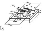
- FIG. 1 is a perspective view of the spin transport element 1.
- FIG. 2 is a sectional view taken along line III-III in FIG.
- the spin transport device 1 includes a silicon oxide film 11 and a silicon channel layer 12 in this order on a silicon substrate 10 when silicon is used as a semiconductor.
- the first nonmagnetic electrode 15A, the first ferromagnetic layer 14A, the second ferromagnetic layer 14B, and the second nonmagnetic electrode 15B are spaced apart from each other in the X-axis direction. Are arranged in this order.
- Tunnel barrier layers 13A and 13B are provided between the silicon channel layer 12 and the first and second ferromagnetic layers 14A and 14B, respectively.
- the silicon channel layer 12, the tunnel barrier film 13A, and the first ferromagnetic layer 14A constitute a spin injection electrode structure IE.
- the silicon oxide film 11, and the silicon channel layer 12, for example, an SOI (Silicon On Insulator) substrate can be used as the silicon substrate 10, the silicon oxide film 11, and the silicon channel layer 12, for example, an SOI (Silicon On Insulator) substrate can be used.
- the film thickness of the silicon oxide film 11 is, for example, 200 nm.
- the silicon channel layer 12 a material to which a dopant for imparting conductivity to silicon is added is used.
- the dopant concentration can be 1.0 ⁇ 10 16 to 1.0 ⁇ 10 22 cm ⁇ 3 .
- the film thickness of the silicon channel layer 12 is, for example, 100 nm.
- the silicon channel layer 12 may be a laminated channel having a predetermined concentration of delta doping. Delta doping means that doping is performed at a high dopant concentration in an extremely thin region of about several nm from the interface, unlike doping in which the dopant is diffused uniformly.
- the silicon channel layer 12 has an inclined portion on the side surface, and the inclination angle ⁇ is 50 degrees to 60 degrees.
- the inclination angle ⁇ is an angle formed by the bottom and side surfaces of the silicon channel layer 12.
- the silicon channel layer 12 can be formed by wet etching, and the upper surface of the silicon channel layer 12 is preferably a (100) plane.
- the silicon channel layer 12 includes a first convex portion 12A, a second convex portion 12B, a third convex portion 12C, a fourth convex portion 12D, and a main portion 12E.
- the first convex portion 12A, the second convex portion 12B, the third convex portion 12C, and the fourth convex portion 12D are portions that extend so as to protrude from the main portion 12E, and have a predetermined interval in the X-axis direction. Are arranged in this order.
- the film thickness H1 of the first convex portion 12A, the second convex portion 12B, the third convex portion 12C, and the fourth convex portion 12D is, for example, 20 nm.
- the film thickness H2 of the main part 12E is, for example, 80 nm.
- a distance L1 between the first convex portion 12A and the third convex portion 12C is, for example, 100 ⁇ m or less.
- the distance d between the central portion of the first convex portion 12A in the X-axis direction and the central portion of the second convex portion 12B in the X-axis direction is preferably equal to or less than the spin diffusion length.
- the spin diffusion length in the silicon channel layer 12 at room temperature (300 K) is approximately 0.8 ⁇ m.
- the tunnel barrier layers 13A and 13B are made of aluminum oxide containing a ⁇ phase (cubic system, defect spinel crystal structure), and are epitaxially grown on the first and second convex portions 12A and 12B of the silicon channel layer.
- the lattice constant (a) of ⁇ -Al 2 O 3 is 7.91 ⁇
- the film thickness of the tunnel barrier layers 13A and 13B is preferably 2.0 nm or less. As a result, a good-quality epitaxial film with few crystal defects (misfit dislocations) can be obtained, so that a coherent tunnel can be realized.
- the thickness of the tunnel barrier layers 13A and 13B is preferably 0.6 nm or more in consideration of the thickness of one atomic layer. When the thickness is less than 0.6 nm, the film thickness is equal to or less than the lattice constant, so that the film quality and withstand voltage are insufficient, and pinholes are easily generated, which is not preferable from the viewpoint of reliability. When the thickness exceeds 2.0 nm, the device resistance is too high and only a very small current can flow, and only a small amount of spin can be injected, which is not practical.
- One of the first ferromagnetic layer 14A and the second ferromagnetic layer 14B functions as an electrode for injecting spin into the silicon channel layer 12, and the other detects the spin conducted through the silicon channel layer 12. Functions as an electrode.
- the first ferromagnetic layer 14A is provided on the tunnel barrier layer 13A.
- the second ferromagnetic layer 14B is provided on the tunnel barrier layer 13B.
- the material of the first ferromagnetic layer 14A and the second ferromagnetic layer 14B includes, for example, at least one element selected from the group consisting of Mn, Co, Fe, and Ni as a main component. Since these materials are ferromagnetic materials having a high spin polarizability, the function as a spin injection electrode or a spin detection electrode can be suitably realized.
- the first ferromagnetic layer 14A and the second ferromagnetic layer 14B preferably have a body-centered cubic (bcc) crystal structure.
- the layer which consists of Heusler alloys may be included.
- the ferromagnetic layer can be epitaxially grown on the tunnel barrier layer in a predetermined crystal orientation, so that the spin polarizability can be further increased.
- the first ferromagnetic layer 14A and the second ferromagnetic layer 14B have a difference in coercive force (reversal magnetic field).
- the first ferromagnetic layer 14A and the second ferromagnetic layer 14B have a rectangular parallelepiped shape with the major axis in the Y-axis direction, and are maintained by shape anisotropy (difference in aspect ratio). A magnetic difference is applied.
- the width (length in the X-axis direction) of the first ferromagnetic layer 14A is, for example, about 350 nm.
- the width (length in the X-axis direction) of the second ferromagnetic layer 14B is, for example, about 2 ⁇ m.
- the first ferromagnetic layer 14A and the second ferromagnetic layer 14B may be provided with an antiferromagnetic layer on one side so that the magnetization of one ferromagnetic layer is fixed in one direction. Furthermore, the aspect which strengthened the exchange coupling with an antiferromagnetic layer by the synthetic pinned structure may be sufficient. Alternatively, the ferromagnetic layer may be made into a single magnetic domain by making the bias magnetic field application layer adjacent to each other.
- One of the first nonmagnetic electrode 15 ⁇ / b> A and the second nonmagnetic electrode 15 ⁇ / b> B functions as an electrode for causing a spin-polarized current to flow through the silicon channel layer 12, and the other uses the spin conducted through the silicon channel layer 12 as a voltage. It functions as an electrode for detection as an output.
- the first nonmagnetic electrode 15A and the second nonmagnetic electrode 15B are provided on the third convex portion 12C and the fourth convex portion 12D of the silicon channel layer 12, respectively.
- the first nonmagnetic electrode 15A and the second nonmagnetic electrode 15B are made of a nonmagnetic metal having a low resistance to Si, such as Al.
- the protective film 7 a is formed on the side surface of the silicon channel layer 12.
- the protective film 7b includes the silicon channel layer 12, the protective film 7a, the tunnel barrier layer 13A, the tunnel barrier layer 13B, the first ferromagnetic layer 14A, the second ferromagnetic layer 14B, the first nonmagnetic electrode 15A, and the second It is formed on the side surface of the nonmagnetic electrode 15B.
- a protective film 7b is formed on the upper surface of the silicon channel layer 12.
- the protective films 7a and 7b are formed in order to insulate and separate the silicon channel layer 12 and to suppress the absorption of spin by wiring or the like. Further, the tunnel barrier layers 13A and 13B lacking in chemical stability are prevented from being exposed to the outside, and function as a protective film for suppressing characteristic fluctuation and deterioration of the spin transport element 1.
- Material of the protective layer 7a and 7b is, for example, SiO 2.
- wirings 18 ⁇ / b> A, 18 ⁇ / b> B, 18 ⁇ / b> C, and 18 ⁇ / b> D are formed on the first nonmagnetic electrode 15 ⁇ / b> A, the first ferromagnetic layer 14 ⁇ / b> A, the second ferromagnetic layer 14 ⁇ / b> B, and the second nonmagnetic electrode 15 ⁇ / b> B.
- Each is provided and routed to the top of the silicon oxide film 11 through the protective film 7b (the inclined side surface of the silicon channel layer 12).
- the material of the wirings 18A, 18B, 18C and 18D is made of a low resistance conductive material such as Cu.
- measurement electrode pads E1, E2, E3, and E4 are provided at the ends of the wirings 18A, 18B, 18C, and 18D, and are formed on the silicon oxide film 11. Yes.
- the material of the electrode pads E1, E2, E3 and E4 is made of a conductive material having high corrosion resistance and low resistance such as Au.
- the electrode pads E1 and E3 are connected to the current source 70, thereby connecting the first ferromagnetic layer 14A, the tunnel barrier layer 13A, the silicon channel layer 12 and the first nonmagnetic electrode 15A.
- a spin-polarized current corresponding to the magnetization direction G1 of the first ferromagnetic layer 14A flows.
- a spin corresponding to the magnetization direction G1 of the first ferromagnetic layer 14A is injected into the silicon channel layer 12, and diffuses as a spin current toward the second ferromagnetic layer 14B. That is, a structure in which current and spin current flow in the X-axis direction of the silicon channel layer 12 can be obtained.
- the spin injected from the first ferromagnetic layer 14A to the silicon channel layer 12 and diffused to the second ferromagnetic layer 14B side is caused by the potential difference from the spin corresponding to the magnetization direction G2 of the second ferromagnetic layer 14B.
- a voltage output is generated at the interface between the channel layer 12 and the second ferromagnetic layer 14B. This voltage output can be detected by connecting the electrode pads E2 and E4 to the output measuring device 80 as shown in FIGS.
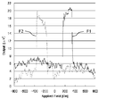
- FIG. 3 shows an example of non-local spin valve measurement results.
- FIG. 3 is a graph showing the relationship between the strength (Oe) of the applied magnetic field B1 in the Y-axis direction and the voltage output ( ⁇ V) detected accordingly.
- F1 shows the case where the external magnetic field B1 is changed from the minus side to the plus side
- F2 shows the case where the external magnetic field B1 is changed from the plus side to the minus side. That is, the resistance is low when the magnetization direction G1 of the first ferromagnetic layer 14A and the magnetization direction G2 of the second ferromagnetic layer 14B are parallel, and the resistance is high when the magnetization direction is antiparallel.
- FIG. 4 is a graph showing the relationship between the strength (Oe) of the applied magnetic field B2 in the Z-axis direction and the voltage output ( ⁇ V) detected accordingly.
- the external magnetic field is zero
- the spin that diffuses through the silicon channel layer 12 does not perform Larmor rotation, and the voltage output becomes an extreme value in order to maintain the injected state. That is, when the magnetization direction G1 of the first ferromagnetic layer 14A and the magnetization direction G2 of the second ferromagnetic layer 14B are parallel, the resistance increases as the magnetic field strength increases.
- the magnetization direction G1 of the first ferromagnetic layer 14A and the magnetization direction G2 of the second ferromagnetic layer 14B are antiparallel, the resistance decreases as the magnetic field strength increases.
- the lattice mismatch with ⁇ -Al 2 O 3 is ⁇ 1.0% and ⁇ 1.4%, respectively, and the same effect as in the present invention can be obtained.
- a gate electrode may be provided between the first ferromagnetic layer 14A and the second ferromagnetic layer 14B. Thereby, the rotation angle of the spin conducted through the silicon channel layer 12 can be controlled by the gate electric field.
- the spin transport element 1 in the present invention can be applied to various spin transport devices such as a magnetic head, a magnetoresistive memory (MRAM), a logic circuit, a nuclear spin memory, a quantum computer, and the like. it can.
- MRAM magnetoresistive memory
- a logic circuit a nuclear spin memory
- quantum computer a quantum computer
- Example 1 Comparative Example 1
- Comparative Example 2 Comparative Example 2
- Example 1 An SOI substrate comprising a silicon substrate, a silicon oxide film (film thickness 200 nm), and a silicon film (film thickness 100 nm) was prepared.
- a dopant channel for imparting conductivity to the silicon film is ion-implanted, annealed at 900 ° C., and diffused and activated to uniformly diffuse a silicon channel having a carrier concentration of 5.0 ⁇ 10 19 cm ⁇ 3.
- a layer was formed.
- the cleaned and planarized SOI substrate surface was formed by flushing the SOI substrate in a molecular beam epitaxy (MBE) apparatus.
- MBE molecular beam epitaxy
- Al 2 O 3 film thickness: 0.8 nm
- Fe film thickness: 13 nm
- Ti an antioxidant film of Fe
- a film thickness of 3 nm was deposited in this order to form a laminate.
- Evaluation after the film formation confirmed that Al 2 O 3 contained a ⁇ phase (cubic crystal, defect spinel crystal structure) and was epitaxially grown on Si.
- the evaluation after film-forming evaluated the crystal structure of the tunnel barrier layer, and the crystal orientation of a laminated film with the X-ray diffraction method (XRD) and the high-resolution transmission electron microscope (HRTEM), respectively.
- XRD X-ray diffraction method
- HRTEM high-resolution transmission electron microscope
- the stacked body was patterned by photolithography and ion milling to expose the silicon channel layer.
- the silicon channel layer was anisotropically wet etched to form a silicon channel layer having an inclined portion on the side surface.
- the size of the silicon channel layer was 23 ⁇ m ⁇ 300 ⁇ m, and the side surface of the silicon channel layer was oxidized.
- the laminate was patterned by photolithography and ion milling to form a spin injection electrode and a spin detection electrode. Further, SiO 2 was formed as a protective film on the side wall of the spin injection electrode and the spin detection electrode and on the exposed portion of the silicon channel layer. Thereafter, the protective film at positions to be the first nonmagnetic electrode and the second nonmagnetic electrode was removed, and a first nonmagnetic electrode and a second nonmagnetic electrode made of Al were formed.
- Comparative Example 1 In Comparative Example 1, a spin transport device was manufactured by the same procedure as in Example 1 except that the film formation conditions of the tunnel barrier layer in Example 1 were changed. After the film formation, Al 2 O 3 was confirmed to be amorphous by the same evaluation as in Example 1.
- Comparative Example 2 In Comparative Example 2, a spin transport device was fabricated by the same procedure as in Example 1 except that the tunnel barrier layer in Example 1 was MgO (film thickness: 0.8 nm). After film formation, the same evaluation as in Example 1 confirmed that MgO has a cubic crystal structure (NaCl-type structure) and is epitaxially grown. At the interface between the silicon channel layer and the tunnel barrier layer, the existence of lattice defects that may be caused by lattice mismatch was confirmed.
- the ferromagnetic layer is limited to Fe in order to make a systematic comparison without depending on the material.
- the ferromagnetic layer Needless to say, it is effective to appropriately change the material.
Landscapes
- Physics & Mathematics (AREA)
- Condensed Matter Physics & Semiconductors (AREA)
- General Physics & Mathematics (AREA)
- Hall/Mr Elements (AREA)
- Magnetic Heads (AREA)
- Mram Or Spin Memory Techniques (AREA)
Priority Applications (1)
| Application Number | Priority Date | Filing Date | Title |
|---|---|---|---|
| US14/378,281 US20150001601A1 (en) | 2012-02-14 | 2013-02-12 | Spin injection electrode structure and spin transport element having the same |
Applications Claiming Priority (2)
| Application Number | Priority Date | Filing Date | Title |
|---|---|---|---|
| JP2012-029253 | 2012-02-14 | ||
| JP2012029253 | 2012-02-14 |
Publications (1)
| Publication Number | Publication Date |
|---|---|
| WO2013122024A1 true WO2013122024A1 (fr) | 2013-08-22 |
Family
ID=48984135
Family Applications (1)
| Application Number | Title | Priority Date | Filing Date |
|---|---|---|---|
| PCT/JP2013/053180 Ceased WO2013122024A1 (fr) | 2012-02-14 | 2013-02-12 | Structure d'électrode pour implantation de spin et élément de transport de spin utilisant celle-ci |
Country Status (3)
| Country | Link |
|---|---|
| US (1) | US20150001601A1 (fr) |
| JP (1) | JPWO2013122024A1 (fr) |
| WO (1) | WO2013122024A1 (fr) |
Cited By (1)
| Publication number | Priority date | Publication date | Assignee | Title |
|---|---|---|---|---|
| WO2022161366A1 (fr) * | 2021-01-29 | 2022-08-04 | 合肥本源量子计算科技有限责任公司 | Dispositif à points quantiques à semi-conducteurs et son procédé de préparation, et procédé de lecture de signal et procédé de manipulation |
Families Citing this family (10)
| Publication number | Priority date | Publication date | Assignee | Title |
|---|---|---|---|---|
| JP5655689B2 (ja) * | 2011-04-21 | 2015-01-21 | Tdk株式会社 | スピン伝導素子 |
| US9825155B2 (en) * | 2013-11-20 | 2017-11-21 | Tdk Corporation | Magnetoresistive element and spin-transport element |
| JP6437265B2 (ja) * | 2014-10-01 | 2018-12-12 | 株式会社東芝 | 磁気ヘッド、磁気記録再生装置、および磁気ヘッドの製造方法 |
| US10132880B2 (en) * | 2014-12-10 | 2018-11-20 | The United States of America, as represented by the Secratary of the Navy | Direct electrical detection of current-induced spin polarization due to spin-momentum locking in topological insulators |
| WO2016099516A1 (fr) * | 2014-12-18 | 2016-06-23 | Intel Corporation | Procédé de fabrication de dispositifs logiques de spin à partir d'empilements magnétiques déposés in situ |
| WO2017090728A1 (fr) | 2015-11-27 | 2017-06-01 | Tdk株式会社 | Élément d'inversion de magnétisation de courant de spin, élément à effet de magnétorésistance, et mémoire magnétique |
| JP2017108067A (ja) | 2015-12-11 | 2017-06-15 | Tdk株式会社 | 磁気抵抗効果素子 |
| WO2017135251A1 (fr) * | 2016-02-02 | 2017-08-10 | 国立研究開発法人物質・材料研究機構 | Jonction de tunnel ferromagnétique, élément à effet magnéto-résistif et dispositif spintronique dans lequel ladite jonction de tunnel ferromagnétique est utilisée, et procédé de fabrication de jonction de tunnel ferromagnétique |
| JP2017139399A (ja) * | 2016-02-05 | 2017-08-10 | Tdk株式会社 | 磁気メモリ |
| KR102453182B1 (ko) | 2016-10-31 | 2022-10-07 | 티에스아이 인코포레이티드 | 저소음 파티클 카운팅을 위한 복합 윅 |
Citations (3)
| Publication number | Priority date | Publication date | Assignee | Title |
|---|---|---|---|---|
| JP2003318462A (ja) * | 2002-04-22 | 2003-11-07 | Matsushita Electric Ind Co Ltd | 磁気抵抗効果素子とこれを用いた磁気ヘッドおよび磁気メモリ |
| JP2010287666A (ja) * | 2009-06-10 | 2010-12-24 | Tdk Corp | スピン伝導素子 |
| JP2010287629A (ja) * | 2009-06-09 | 2010-12-24 | Tdk Corp | 半導体スピンデバイス |
Family Cites Families (3)
| Publication number | Priority date | Publication date | Assignee | Title |
|---|---|---|---|---|
| DE602007011491D1 (de) * | 2006-10-10 | 2011-02-03 | Univ Plymouth | Verfahren zur detektion der ladungsträgerspinpolarisation und vorrichtung dafür |
| US20090141409A1 (en) * | 2007-12-03 | 2009-06-04 | Santos Tiffany S | Spin filter spintronic devices |
| WO2010119928A1 (fr) * | 2009-04-16 | 2010-10-21 | 独立行政法人物質・材料研究機構 | Structure de jonction tunnel ferromagnétique, et élément à effet magnétorésistif et dispositif spintronique comprenant chacun cette structure |
-
2013
- 2013-02-12 WO PCT/JP2013/053180 patent/WO2013122024A1/fr not_active Ceased
- 2013-02-12 JP JP2013558681A patent/JPWO2013122024A1/ja active Pending
- 2013-02-12 US US14/378,281 patent/US20150001601A1/en not_active Abandoned
Patent Citations (3)
| Publication number | Priority date | Publication date | Assignee | Title |
|---|---|---|---|---|
| JP2003318462A (ja) * | 2002-04-22 | 2003-11-07 | Matsushita Electric Ind Co Ltd | 磁気抵抗効果素子とこれを用いた磁気ヘッドおよび磁気メモリ |
| JP2010287629A (ja) * | 2009-06-09 | 2010-12-24 | Tdk Corp | 半導体スピンデバイス |
| JP2010287666A (ja) * | 2009-06-10 | 2010-12-24 | Tdk Corp | スピン伝導素子 |
Cited By (1)
| Publication number | Priority date | Publication date | Assignee | Title |
|---|---|---|---|---|
| WO2022161366A1 (fr) * | 2021-01-29 | 2022-08-04 | 合肥本源量子计算科技有限责任公司 | Dispositif à points quantiques à semi-conducteurs et son procédé de préparation, et procédé de lecture de signal et procédé de manipulation |
Also Published As
| Publication number | Publication date |
|---|---|
| US20150001601A1 (en) | 2015-01-01 |
| JPWO2013122024A1 (ja) | 2015-05-11 |
Similar Documents
| Publication | Publication Date | Title |
|---|---|---|
| WO2013122024A1 (fr) | Structure d'électrode pour implantation de spin et élément de transport de spin utilisant celle-ci | |
| JP6733496B2 (ja) | スピン軌道トルク型磁化反転素子及び磁気メモリ | |
| Dankert et al. | Tunnel magnetoresistance with atomically thin two-dimensional hexagonal boron nitride barriers | |
| JP4455558B2 (ja) | スピンmosfet | |
| EP2434556B1 (fr) | Structure à jonction de tunnel ferromagnétique et élément magnétorésistif l'utilisant | |
| KR102751409B1 (ko) | 스핀궤도 토크(spin-orbit torque, SOT) 기반 자기 터널 접합 및 이의 제조 방법 | |
| JP5765440B2 (ja) | スピン注入電極構造、スピン伝導素子及びスピン伝導デバイス | |
| KR102560822B1 (ko) | 스핀궤도 토크(spin-orbit torque, SOT) 기반 자기 터널 접합 및 이의 제조 방법 | |
| JP2010239011A (ja) | スピン注入構造及びそれを用いたスピン伝導デバイス | |
| JP5688526B2 (ja) | 強磁性積層構造の製造方法 | |
| Oki et al. | Lateral spin valves with two-different Heusler-alloy electrodes on the same platform | |
| JP6236791B2 (ja) | スピン注入電極構造及びそれを用いたスピン伝導素子 | |
| Belmoubarik et al. | Epitaxial wurtzite-MgZnO barrier based magnetic tunnel junctions deposited on a metallic ferromagnetic electrode | |
| JP5294043B2 (ja) | トンネル磁気抵抗素子 | |
| JP6294984B2 (ja) | トンネル層 | |
| JP6299897B2 (ja) | トンネル層 | |
| JP6394759B2 (ja) | 積層体 | |
| JP6093561B2 (ja) | スピン注入電極構造、及びスピン伝導素子 | |
| JP6093560B2 (ja) | スピン注入電極構造、及びスピン伝導素子 | |
| JP6958691B2 (ja) | トンネル層 | |
| JP2007027441A (ja) | 強磁性半導体交換結合膜 | |
| Singh et al. | Giant magnetoresistance in an all-oxide spacerless junction | |
| TWI917895B (zh) | 磁性元件及磁性記憶體 | |
| JP6757446B2 (ja) | トンネル層 | |
| JP6534462B2 (ja) | トンネル層 |
Legal Events
| Date | Code | Title | Description |
|---|---|---|---|
| 121 | Ep: the epo has been informed by wipo that ep was designated in this application |
Ref document number: 13749811 Country of ref document: EP Kind code of ref document: A1 |
|
| ENP | Entry into the national phase |
Ref document number: 2013558681 Country of ref document: JP Kind code of ref document: A |
|
| WWE | Wipo information: entry into national phase |
Ref document number: 14378281 Country of ref document: US |
|
| NENP | Non-entry into the national phase |
Ref country code: DE |
|
| 122 | Ep: pct application non-entry in european phase |
Ref document number: 13749811 Country of ref document: EP Kind code of ref document: A1 |