WO2013122147A1 - Procédé de formation d'un film de cnt (nanotubes de carbone) - Google Patents
Procédé de formation d'un film de cnt (nanotubes de carbone) Download PDFInfo
- Publication number
- WO2013122147A1 WO2013122147A1 PCT/JP2013/053540 JP2013053540W WO2013122147A1 WO 2013122147 A1 WO2013122147 A1 WO 2013122147A1 JP 2013053540 W JP2013053540 W JP 2013053540W WO 2013122147 A1 WO2013122147 A1 WO 2013122147A1
- Authority
- WO
- WIPO (PCT)
- Prior art keywords
- cnt
- cnt film
- dispersion
- film
- silica
- Prior art date
- Legal status (The legal status is an assumption and is not a legal conclusion. Google has not performed a legal analysis and makes no representation as to the accuracy of the status listed.)
- Ceased
Links
Images
Classifications
-
- C—CHEMISTRY; METALLURGY
- C04—CEMENTS; CONCRETE; ARTIFICIAL STONE; CERAMICS; REFRACTORIES
- C04B—LIME, MAGNESIA; SLAG; CEMENTS; COMPOSITIONS THEREOF, e.g. MORTARS, CONCRETE OR LIKE BUILDING MATERIALS; ARTIFICIAL STONE; CERAMICS; REFRACTORIES; TREATMENT OF NATURAL STONE
- C04B35/00—Shaped ceramic products characterised by their composition; Ceramics compositions; Processing powders of inorganic compounds preparatory to the manufacturing of ceramic products
- C04B35/622—Forming processes; Processing powders of inorganic compounds preparatory to the manufacturing of ceramic products
- C04B35/62218—Forming processes; Processing powders of inorganic compounds preparatory to the manufacturing of ceramic products obtaining ceramic films, e.g. by using temporary supports
-
- B—PERFORMING OPERATIONS; TRANSPORTING
- B05—SPRAYING OR ATOMISING IN GENERAL; APPLYING FLUENT MATERIALS TO SURFACES, IN GENERAL
- B05D—PROCESSES FOR APPLYING FLUENT MATERIALS TO SURFACES, IN GENERAL
- B05D3/00—Pretreatment of surfaces to which liquids or other fluent materials are to be applied; After-treatment of applied coatings, e.g. intermediate treating of an applied coating preparatory to subsequent applications of liquids or other fluent materials
- B05D3/10—Pretreatment of surfaces to which liquids or other fluent materials are to be applied; After-treatment of applied coatings, e.g. intermediate treating of an applied coating preparatory to subsequent applications of liquids or other fluent materials by other chemical means
- B05D3/107—Post-treatment of applied coatings
-
- B—PERFORMING OPERATIONS; TRANSPORTING
- B82—NANOTECHNOLOGY
- B82Y—SPECIFIC USES OR APPLICATIONS OF NANOSTRUCTURES; MEASUREMENT OR ANALYSIS OF NANOSTRUCTURES; MANUFACTURE OR TREATMENT OF NANOSTRUCTURES
- B82Y30/00—Nanotechnology for materials or surface science, e.g. nanocomposites
-
- B—PERFORMING OPERATIONS; TRANSPORTING
- B82—NANOTECHNOLOGY
- B82Y—SPECIFIC USES OR APPLICATIONS OF NANOSTRUCTURES; MEASUREMENT OR ANALYSIS OF NANOSTRUCTURES; MANUFACTURE OR TREATMENT OF NANOSTRUCTURES
- B82Y40/00—Manufacture or treatment of nanostructures
-
- C—CHEMISTRY; METALLURGY
- C01—INORGANIC CHEMISTRY
- C01B—NON-METALLIC ELEMENTS; COMPOUNDS THEREOF; METALLOIDS OR COMPOUNDS THEREOF NOT COVERED BY SUBCLASS C01C
- C01B32/00—Carbon; Compounds thereof
- C01B32/15—Nano-sized carbon materials
- C01B32/158—Carbon nanotubes
- C01B32/168—After-treatment
- C01B32/174—Derivatisation; Solubilisation; Dispersion in solvents
-
- C—CHEMISTRY; METALLURGY
- C04—CEMENTS; CONCRETE; ARTIFICIAL STONE; CERAMICS; REFRACTORIES
- C04B—LIME, MAGNESIA; SLAG; CEMENTS; COMPOSITIONS THEREOF, e.g. MORTARS, CONCRETE OR LIKE BUILDING MATERIALS; ARTIFICIAL STONE; CERAMICS; REFRACTORIES; TREATMENT OF NATURAL STONE
- C04B35/00—Shaped ceramic products characterised by their composition; Ceramics compositions; Processing powders of inorganic compounds preparatory to the manufacturing of ceramic products
- C04B35/515—Shaped ceramic products characterised by their composition; Ceramics compositions; Processing powders of inorganic compounds preparatory to the manufacturing of ceramic products based on non-oxide ceramics
- C04B35/52—Shaped ceramic products characterised by their composition; Ceramics compositions; Processing powders of inorganic compounds preparatory to the manufacturing of ceramic products based on non-oxide ceramics based on carbon, e.g. graphite
-
- H—ELECTRICITY
- H01—ELECTRIC ELEMENTS
- H01B—CABLES; CONDUCTORS; INSULATORS; SELECTION OF MATERIALS FOR THEIR CONDUCTIVE, INSULATING OR DIELECTRIC PROPERTIES
- H01B1/00—Conductors or conductive bodies characterised by the conductive materials; Selection of materials as conductors
- H01B1/14—Conductive material dispersed in non-conductive inorganic material
- H01B1/18—Conductive material dispersed in non-conductive inorganic material the conductive material comprising carbon-silicon compounds, carbon or silicon
-
- C—CHEMISTRY; METALLURGY
- C04—CEMENTS; CONCRETE; ARTIFICIAL STONE; CERAMICS; REFRACTORIES
- C04B—LIME, MAGNESIA; SLAG; CEMENTS; COMPOSITIONS THEREOF, e.g. MORTARS, CONCRETE OR LIKE BUILDING MATERIALS; ARTIFICIAL STONE; CERAMICS; REFRACTORIES; TREATMENT OF NATURAL STONE
- C04B2235/00—Aspects relating to ceramic starting mixtures or sintered ceramic products
- C04B2235/02—Composition of constituents of the starting material or of secondary phases of the final product
- C04B2235/50—Constituents or additives of the starting mixture chosen for their shape or used because of their shape or their physical appearance
- C04B2235/52—Constituents or additives characterised by their shapes
- C04B2235/5284—Hollow fibers, e.g. nanotubes
- C04B2235/5288—Carbon nanotubes
Definitions
- the present invention relates to a method for forming a CNT film.
- the transparent conductive film is applied to a touch panel, a solar cell, an antistatic film, an electromagnetic wave shielding material, a planar heating element, and the like.
- ITO tin-doped indium oxide
- alternative transparent conductive films have been studied.
- alternative transparent conductive film candidates include a carbon nanotube (hereinafter referred to as CNT) film and zinc oxide (hereinafter referred to as ZnO).
- CNT has a feature that it can be applied to a flexible film that is difficult with ITO or ZnO.
- the CNT film can be obtained by applying and drying a dispersion in which CNTs are dispersed on a substrate by a dip coating method, a spin coating method, a spray coating method, or the like. In order to obtain a CNT film having excellent characteristics by this method, it is necessary to prepare a dispersion in which CNTs are stably dispersed.
- Non-patent Document 1 a method of treating CNT with an acid
- Patent Document 2 a method of treating with CNT
- Patent Document 2 a method of adding a surfactant
- CNTs are surface-treated with acid or plasma, defects are formed on the CNT surface or the CNTs themselves are cut. Therefore, the excellent characteristics inherent in CNTs (electric conductivity, thermal conductivity, mechanical Strength).
- a surfactant that is difficult to remove remains in the CNT film, and the conductivity of the CNT film decreases.
- the method for forming a CNT film of the present invention includes forming a CNT film by applying and drying a dispersion containing CNT and silica colloid on a substrate. According to the method for forming a CNT film of the present invention, since it is not necessary to surface-treat the CNT with acid or plasma, defects are not generated on the CNT surface or the CNT is not cut. As a result, a CNT film having excellent characteristics (electric conductivity, thermal conductivity, mechanical strength, etc.) can be formed. In addition, since it is not necessary to add a surfactant to the CNT dispersion, a surfactant that is difficult to remove does not remain in the CNT film. As a result, a CNT film having excellent characteristics (electric conductivity, thermal conductivity, mechanical strength, etc.) can be formed.
- the method for forming a CNT film of the present invention it is preferable to remove the silica colloid from the CNT film using an alkaline aqueous solution or hydrofluoric acid.
- the concentration of the aqueous alkali solution or hydrofluoric acid can be adjusted as appropriate, and can be, for example, in the range of 0.1 to 1 mol / l.
- Examples of a method for removing the silica colloid from the CNT film using an alkaline aqueous solution or hydrofluoric acid include a method of immersing the CNT film in an alkaline aqueous solution or hydrofluoric acid. In this case, the immersion time can be adjusted as appropriate, and can be, for example, in the range of 1 to 30 minutes.
- the alkaline aqueous solution is not particularly limited as long as it can remove the silica colloid, and examples thereof include a sodium hydroxide aqueous solution and a potassium hydroxide aqueous solution.
- the concentration of the silica colloid in the dispersion is preferably in the range of 0.001 to 5% by weight, and more preferably in the range of 0.001 to 0.1%. By being in this range, CNT can be stably dispersed in the dispersion liquid, and the characteristics (for example, electrical conductivity) of the formed CNT film are further improved.
- the CNT concentration in the dispersion is preferably in the range of 1 ⁇ 10 ⁇ 5 to 5 wt%. By being in this range, the characteristics (for example, electrical conductivity) of the formed CNT film are further improved.
- the solvent (dispersion medium) of the dispersion can be appropriately selected, and examples thereof include water, volatile organic solvents (for example, THF (tetrahydrofuran), ethanol, etc.), or a mixture thereof.
- a surfactant and other additive components may be blended within a range that does not significantly deteriorate the properties of the CNT film.
- the said base material is not specifically limited,
- the base material which consists of glass, resin (for example, PET) etc. can be used.
- the coating method is not particularly limited, and for example, a dip coating method, a spin coating method, a spray method, or the like can be used. Further, the substrate may be heated during the formation of the CNT film.
- a silica colloid solution having a concentration of 0.01% by weight, a silica colloid solution having a SiO 2 concentration of 0.05% by weight, and a silica colloid solution having a SiO 2 concentration of 0.1% by weight were prepared.
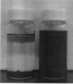
- a single-walled CNT (manufactured by Unidym) is added to each of the five types of silica colloid solutions prepared in (1-1) and subjected to ultrasonic treatment, thereby including CNT and silica colloid.
- Five types of dispersions were prepared. Below, the prepared dispersion liquid is described as follows.
- Dispersion A1 A dispersion prepared using a silica colloid solution having a SiO 2 concentration of 0.001% by weight.
- Dispersion A2 A dispersion prepared using a silica colloid solution having a SiO 2 concentration of 0.005% by weight.
- Dispersion A3 Dispersion prepared using a silica colloid solution having a SiO 2 concentration of 0.01% by weight.
- Dispersion A4 A dispersion prepared using a silica colloid solution having a SiO 2 concentration of 0.05% by weight.
- Dispersion A5 A dispersion prepared using a silica colloid solution having a SiO 2 concentration of 0.1% by weight.
- the composition of the dispersions A1 to A5 is as follows. ⁇ Dispersion A1> Single-walled CNT: 0.01% by weight Silica: 0.001% by weight Water: 21.939% by weight THF: 78.05% by weight ⁇ Dispersion A2> Single-walled CNT: 0.01% by weight Silica: 0.005% by weight Water: 21.935% by weight THF: 78.05% by weight ⁇ Dispersion A3> Single-walled CNT: 0.01% by weight Silica: 0.01% by weight Water: 21.930% by weight THF: 78.05% by weight ⁇ Dispersion A4> Single-walled CNT: 0.01% by weight Silica: 0.05% by weight Water: 21.89% by weight THF: 78.05% by weight ⁇ Dispersion A5> Single-walled CNT: 0.01% by weight Silica: 0.11% by weight Water
- CNT film (2-1) A dispersion (any one of dispersions A1 to A5) was applied to a PET film having a thickness of 100 ⁇ m by a dip coating method and dried. The dispersion was applied and dried repeatedly a predetermined number of times (any number of 50 times, 100 times, 200 times, and 400 times). Through the above steps, a CNT film (silica unremoved) was formed.
- the resistance value of the CNT film was measured using a four-terminal resistance meter (Loresta GP manufactured by Mitsubishi Chemical). Moreover, the transmittance
- the upper value in each frame represents the resistance value ( ⁇ ), and the lower value represents the transmittance (%).
- the dispersion liquid A4 was used as the dispersion liquid, and the CNT film was coated and dried 200 times. A step of removing the colloid was performed to form a CNT film (after silica removal).
- one of the following three methods was performed.
- One of them is a method of removing the silica colloid by immersing the above CNT film (silica unremoved) in a sodium hydroxide aqueous solution having a concentration of 1 mol / l for 30 minutes.
- Another method is a method in which the CNT film (silica unremoved) is immersed in an aqueous potassium hydroxide solution having a concentration of 1 mol / l for 30 minutes to remove the silica colloid.
- the remaining one method is a method of removing the silica colloid by immersing the CNT film (silica unremoved) in hydrofluoric acid having a concentration of 1 mol / l for 30 minutes.
- the resistance value ( ⁇ ) of the CNT film was measured using a four-terminal resistance meter (Loresta GP manufactured by Mitsubishi Chemical). The results are shown in Table 2. Table 2 also shows the resistance value ( ⁇ ) of the CNT film before the step of removing the silica colloid.
- a step of removing the silica colloid was performed on the CNT film formed in (2-1) (silica unremoved) to form a CNT film (after silica removal).
- the step of removing the silica colloid involves immersing the CNT film in a sodium hydroxide aqueous solution for a predetermined time.
- the combination of the type of CNT film (silica unremoved) that is, the type of dispersion used to form the CNT film) and the conditions for removing the silica colloid (concentration of sodium hydroxide aqueous solution, immersion time) As shown in Table 3.
- membrane is 200 times in all.
- the solvent of the dispersions A1 to A5 may be only water (without THF). In that case, substantially the same effect can be obtained.
- the CNT film may be formed on a resin film other than PET or on a glass substrate. In that case, substantially the same effect can be obtained.
- other application methods for example, a spray method, a spin coat method, etc.
- the CNT film may be compressed. By doing so, the characteristics of the CNT film are further improved.
- a method other than the method of immersing in an alkaline aqueous solution or hydrofluoric acid may be used.
- a method of applying (or spraying) an alkaline aqueous solution or hydrofluoric acid to the surface of the CNT film may be used.
Landscapes
- Chemical & Material Sciences (AREA)
- Engineering & Computer Science (AREA)
- Nanotechnology (AREA)
- Materials Engineering (AREA)
- Organic Chemistry (AREA)
- Inorganic Chemistry (AREA)
- Manufacturing & Machinery (AREA)
- Physics & Mathematics (AREA)
- General Physics & Mathematics (AREA)
- Crystallography & Structural Chemistry (AREA)
- Condensed Matter Physics & Semiconductors (AREA)
- Ceramic Engineering (AREA)
- Composite Materials (AREA)
- Dispersion Chemistry (AREA)
- Structural Engineering (AREA)
- General Chemical & Material Sciences (AREA)
- Chemical Kinetics & Catalysis (AREA)
- Carbon And Carbon Compounds (AREA)
- Nonlinear Science (AREA)
- Manufacturing Of Electric Cables (AREA)
- Mathematical Physics (AREA)
- Optics & Photonics (AREA)
- Silicon Compounds (AREA)
- Paints Or Removers (AREA)
Priority Applications (4)
| Application Number | Priority Date | Filing Date | Title |
|---|---|---|---|
| KR1020147024257A KR20140146058A (ko) | 2012-02-14 | 2013-02-14 | Cnt막의 형성 방법 |
| US14/378,919 US9999903B2 (en) | 2012-02-14 | 2013-02-14 | Method for forming CNT (carbon nanotube) film |
| CN201380008982.2A CN104125926A (zh) | 2012-02-14 | 2013-02-14 | Cnt膜的形成方法 |
| HK15102401.2A HK1201809A1 (en) | 2012-02-14 | 2013-02-14 | Method for forming cnt film |
Applications Claiming Priority (2)
| Application Number | Priority Date | Filing Date | Title |
|---|---|---|---|
| JP2012029687A JP5953569B2 (ja) | 2012-02-14 | 2012-02-14 | Cnt膜の形成方法 |
| JP2012-029687 | 2012-02-14 |
Publications (1)
| Publication Number | Publication Date |
|---|---|
| WO2013122147A1 true WO2013122147A1 (fr) | 2013-08-22 |
Family
ID=48984256
Family Applications (1)
| Application Number | Title | Priority Date | Filing Date |
|---|---|---|---|
| PCT/JP2013/053540 Ceased WO2013122147A1 (fr) | 2012-02-14 | 2013-02-14 | Procédé de formation d'un film de cnt (nanotubes de carbone) |
Country Status (6)
| Country | Link |
|---|---|
| US (1) | US9999903B2 (fr) |
| JP (1) | JP5953569B2 (fr) |
| KR (1) | KR20140146058A (fr) |
| CN (1) | CN104125926A (fr) |
| HK (1) | HK1201809A1 (fr) |
| WO (1) | WO2013122147A1 (fr) |
Families Citing this family (2)
| Publication number | Priority date | Publication date | Assignee | Title |
|---|---|---|---|---|
| CN105268339B (zh) * | 2015-10-20 | 2018-04-24 | 深圳大学 | 碳纳米管分散液和碳纳米管水泥基复合材料的制备方法 |
| WO2025057653A1 (fr) * | 2023-09-11 | 2025-03-20 | Jsr株式会社 | Procédé de fabrication de film électroconducteur, panneau tactile et panneau d'affichage |
Citations (3)
| Publication number | Priority date | Publication date | Assignee | Title |
|---|---|---|---|---|
| JP2003303539A (ja) * | 2002-04-10 | 2003-10-24 | Mitsubishi Electric Corp | 電子放出源およびその製造方法 |
| JP2008037919A (ja) * | 2006-08-02 | 2008-02-21 | Mitsubishi Rayon Co Ltd | カーボンナノチューブ含有組成物とそれから得られる複合体 |
| JP2008177165A (ja) * | 2007-01-17 | 2008-07-31 | Samsung Electronics Co Ltd | カーボンナノチューブの網目状薄膜を含むカーボンナノチューブパターンの透明電極、及びその製造方法 |
Family Cites Families (2)
| Publication number | Priority date | Publication date | Assignee | Title |
|---|---|---|---|---|
| JP2003300715A (ja) | 2001-11-14 | 2003-10-21 | Toray Ind Inc | 多層カーボンナノチューブ、分散液、溶液および組成物、これらの製造方法、ならびに粉末状カーボンナノチューブ |
| JP2010013312A (ja) | 2008-07-03 | 2010-01-21 | Japan Science & Technology Agency | カーボンナノチューブ分散剤、カーボンナノチューブ分散液およびその製造方法 |
-
2012
- 2012-02-14 JP JP2012029687A patent/JP5953569B2/ja active Active
-
2013
- 2013-02-14 HK HK15102401.2A patent/HK1201809A1/xx unknown
- 2013-02-14 US US14/378,919 patent/US9999903B2/en active Active
- 2013-02-14 KR KR1020147024257A patent/KR20140146058A/ko not_active Ceased
- 2013-02-14 CN CN201380008982.2A patent/CN104125926A/zh active Pending
- 2013-02-14 WO PCT/JP2013/053540 patent/WO2013122147A1/fr not_active Ceased
Patent Citations (3)
| Publication number | Priority date | Publication date | Assignee | Title |
|---|---|---|---|---|
| JP2003303539A (ja) * | 2002-04-10 | 2003-10-24 | Mitsubishi Electric Corp | 電子放出源およびその製造方法 |
| JP2008037919A (ja) * | 2006-08-02 | 2008-02-21 | Mitsubishi Rayon Co Ltd | カーボンナノチューブ含有組成物とそれから得られる複合体 |
| JP2008177165A (ja) * | 2007-01-17 | 2008-07-31 | Samsung Electronics Co Ltd | カーボンナノチューブの網目状薄膜を含むカーボンナノチューブパターンの透明電極、及びその製造方法 |
Non-Patent Citations (1)
| Title |
|---|
| DONG KEE YI: "Ordered Array of Linear and Spherical Nanomaterials in a Film Formation via Self Assembly", JOURNAL OF NANOSCIENCE AND NANOTECHNOLOGY, vol. 10, 2010, pages 4690 - 4695 * |
Also Published As
| Publication number | Publication date |
|---|---|
| JP2013166662A (ja) | 2013-08-29 |
| US9999903B2 (en) | 2018-06-19 |
| KR20140146058A (ko) | 2014-12-24 |
| JP5953569B2 (ja) | 2016-07-20 |
| HK1201809A1 (en) | 2015-09-11 |
| CN104125926A (zh) | 2014-10-29 |
| US20150174611A1 (en) | 2015-06-25 |
Similar Documents
| Publication | Publication Date | Title |
|---|---|---|
| JP7120973B2 (ja) | 融着ネットワークを有する透明導電性フィルムの形成のための金属ナノワイヤーインク | |
| US8999205B2 (en) | Metal nanowires with high linearity, method for producing the metal nanowires and transparent conductive film including the metal nanowires | |
| Yang et al. | Robust and smooth UV-curable layer overcoated AgNW flexible transparent conductor for EMI shielding and film heater | |
| JP6179923B2 (ja) | カーボンナノチューブ複合体、カーボンナノチューブ分散液及びそれらの製造方法、カーボンナノチューブの分散方法、並びに、透明電極及びその製造方法 | |
| US9960293B2 (en) | Method for manufacturing a transparent conductive electrode using carbon nanotube films | |
| US10029916B2 (en) | Metal nanowire networks and transparent conductive material | |
| JP2011504280A (ja) | 導電性が改善された透明導電性フィルム及びその製造方法 | |
| CN104861785B (zh) | 高分散碳纳米管复合导电墨水 | |
| CN107221387B (zh) | 基于短暂性构架的高电导率石墨烯薄膜的制备方法 | |
| CN110791136A (zh) | 一种银纳米线涂布溶液及透明导电薄膜 | |
| JP2019036599A (ja) | 熱電変換材料の製造方法、熱電変換素子の製造方法及び熱電変換材料の改質方法 | |
| JP5326336B2 (ja) | 導電体及びその製造方法 | |
| CN106575003B (zh) | 窗户用隔热薄膜、窗户用隔热玻璃及窗户 | |
| JP5953569B2 (ja) | Cnt膜の形成方法 | |
| KR101190206B1 (ko) | 투명도전막 및 그 제조방법 | |
| KR101514276B1 (ko) | 탄소나노튜브와 그래핀산화물이 혼합된 나노카본 기반 일체형 전도성 촉매전극의 제조방법 및 이에 의해 제조된 촉매전극 | |
| CN105390183B (zh) | 含石墨烯的柔性透明导电薄膜及其制备方法 | |
| KR20180004204A (ko) | 다층 투명 전도성 판상 스택의 기계적 보강을 위한 카본 나노튜브계 하이브리드 필름 | |
| CN103137238B (zh) | 透明导电膜及其形成方法 | |
| JP2016124762A (ja) | グラフェン/シリカ複合体の製造方法およびその方法により製造されたグラフェン/シリカ複合体 | |
| KR101300774B1 (ko) | 탄소 나노 튜브 및 아크릴계 수성 중합체를 함유하는 조성물 및 이를 이용한 전도성 투명 전극 | |
| KR20130003467A (ko) | 탄소나노튜브를 이용한 투명 전도성 필름 및 그 제조방법 | |
| KR20110071539A (ko) | 투명도전막 및 그 제조방법 | |
| CN106517812B (zh) | 绒面透明导电的FTO/Gr-CNTs复合薄膜及其制备方法 | |
| JP5780544B2 (ja) | 導電体の製造方法 |
Legal Events
| Date | Code | Title | Description |
|---|---|---|---|
| 121 | Ep: the epo has been informed by wipo that ep was designated in this application |
Ref document number: 13748632 Country of ref document: EP Kind code of ref document: A1 |
|
| NENP | Non-entry into the national phase |
Ref country code: DE |
|
| WWE | Wipo information: entry into national phase |
Ref document number: 14378919 Country of ref document: US |
|
| ENP | Entry into the national phase |
Ref document number: 20147024257 Country of ref document: KR Kind code of ref document: A |
|
| 122 | Ep: pct application non-entry in european phase |
Ref document number: 13748632 Country of ref document: EP Kind code of ref document: A1 |