WO2013122221A1 - 積分型ad変換装置およびcmosイメージセンサ - Google Patents
積分型ad変換装置およびcmosイメージセンサ Download PDFInfo
- Publication number
- WO2013122221A1 WO2013122221A1 PCT/JP2013/053734 JP2013053734W WO2013122221A1 WO 2013122221 A1 WO2013122221 A1 WO 2013122221A1 JP 2013053734 W JP2013053734 W JP 2013053734W WO 2013122221 A1 WO2013122221 A1 WO 2013122221A1
- Authority
- WO
- WIPO (PCT)
- Prior art keywords
- output
- signal
- converter
- integral
- time
- Prior art date
- Legal status (The legal status is an assumption and is not a legal conclusion. Google has not performed a legal analysis and makes no representation as to the accuracy of the status listed.)
- Ceased
Links
Images




Classifications
-
- H—ELECTRICITY
- H03—ELECTRONIC CIRCUITRY
- H03M—CODING; DECODING; CODE CONVERSION IN GENERAL
- H03M1/00—Analogue/digital conversion; Digital/analogue conversion
- H03M1/002—Provisions or arrangements for saving power, e.g. by allowing a sleep mode, using lower supply voltage for downstream stages, using multiple clock domains or by selectively turning on stages when needed
-
- G—PHYSICS
- G04—HOROLOGY
- G04F—TIME-INTERVAL MEASURING
- G04F10/00—Apparatus for measuring unknown time intervals by electric means
- G04F10/005—Time-to-digital converters [TDC]
-
- H—ELECTRICITY
- H03—ELECTRONIC CIRCUITRY
- H03M—CODING; DECODING; CODE CONVERSION IN GENERAL
- H03M1/00—Analogue/digital conversion; Digital/analogue conversion
- H03M1/12—Analogue/digital converters
- H03M1/14—Conversion in steps with each step involving the same or a different conversion means and delivering more than one bit
-
- H—ELECTRICITY
- H03—ELECTRONIC CIRCUITRY
- H03M—CODING; DECODING; CODE CONVERSION IN GENERAL
- H03M1/00—Analogue/digital conversion; Digital/analogue conversion
- H03M1/12—Analogue/digital converters
- H03M1/50—Analogue/digital converters with intermediate conversion to time interval
- H03M1/56—Input signal compared with linear ramp
-
- H—ELECTRICITY
- H04—ELECTRIC COMMUNICATION TECHNIQUE
- H04N—PICTORIAL COMMUNICATION, e.g. TELEVISION
- H04N25/00—Circuitry of solid-state image sensors [SSIS]; Control thereof
- H04N25/70—SSIS architectures; Circuits associated therewith
- H04N25/76—Addressed sensors, e.g. MOS or CMOS sensors
Definitions
- the present invention relates to an integral AD converter and a CMOS image sensor.
- This single slope type AD converter compares an analog input voltage with a reference voltage having a ramp waveform that changes linearly with respect to time by a comparator, and the counter circuit compares the time until the output of the comparator is inverted. It counts and outputs the counted result as a digital value.
- TDC Time to Digital Converter
- the integral AD converter 101 described in Non-Patent Document 1 includes a comparator 10, a counter 30, a TDC 140, and a DLL (Delay Locked Loop) 50, as shown in FIG.
- the comparator 10 compares the analog input signal vin with a reference signal ramp having a ramp waveform that changes linearly with respect to time, and outputs the comparison result as an output voltage vcomp.
- the reference signal ramp changes linearly with the passage of time, and the magnitude relationship between the analog input signal vin and the reference signal ramp is reversed at time t inv .
- the output vcomp of the comparator 10 is inverted.
- the counter 30 counts the time up to the time t inv based on the input reference clock signal, and outputs the counted result as the output result out2.
- FIG. 12B shows an enlarged view of the vicinity of time t inv in FIG.
- the TDC 140 measures the time t from the start of the period T to the time t inv within one period T of the reference clock, and outputs the measurement result as an output result out1.
- the DLL 50 outputs four clock signals CLKA, CLKB, CLKC, and CLKD having the same frequency as the reference clock signal and a phase changed by 45 degrees.
- the TDC 140 latches the values of the four clock signals CLKA, CLKB, CLKC, and CLKD at the time t inv when the output of the comparator 10 is inverted. For example, in the case of FIG.
- the magnitude relationship between the analog input signal vin and the reference signal ramp is reversed at time t inv and the output vcomp of the comparator 10 is inverted.
- CLKA is at a high level
- These values of CLKA, CLKB, CLKC, and CLKD are latched.
- the TDC 140 uses the phase information indicating whether CLKA, CLKB, CLKC, and CLKD are each at the high level or the low level, the TDC 140 determines the time within one clock cycle of the time t inv from one clock cycle. Also measure in fine time units.
- the AD converter described in Patent Document 1 also includes a comparator 10, a counter 30, and a TDC 140, and performs the same processing as that of the integral AD converter 101 described in Non-Patent Document 1.
- the TDC 140 has a flip-flop driven by a clock signal having a plurality of phases, so that the power consumption of the TDC 140 increases, and as a result, the power consumption of the integrating AD converter.
- the power consumption of the integral AD converter increases as the number of clock signals increases. Become.
- an object of the present invention is to provide an integral AD converter and a CMOS image sensor that can reduce power consumption while improving at least one of conversion accuracy and conversion speed.
- an integrating AD converter compares a reference voltage and an input voltage of a ramp waveform that changes linearly with respect to time, and compares the reference voltage and the input voltage.
- a comparator that outputs a comparison signal
- a multi-phase clock generation circuit that generates a plurality of clock signals including a main clock signal and a clock signal having a phase different from that of the main clock signal, and a comparison signal output from the comparator
- a delay adjustment circuit that outputs the signal after being delayed by one or more cycles of the signal, and a signal output from the delay adjustment circuit and a main clock signal from the time the ramp waveform starts to change until the output from the delay adjustment circuit is inverted.
- the multi-phase clock generation circuit generates a counter at the timing when the output signal of the delay adjustment circuit and the counter that outputs the counted result as the upper bits and the delay adjustment circuit are inverted.
- a time quantizer that latches a plurality of clock signals and outputs the result of decoding the latched values as lower bits, and the time quantizer is at a timing at which the comparison signal output from the comparator is inverted. The operation is started, and after the lower bits are output at the timing when the output signal of the delay adjustment circuit is inverted, the operation is stopped.
- the delay adjustment circuit delays the comparison signal output from the comparator by a time equal to or longer than one period of the main clock signal, and the time quantizer includes the comparator.
- the operation starts at the timing when the output signal is inverted, and stops at the timing when the output signal of the delay adjustment circuit is inverted. For this reason, since the time quantizer can be operated for a required time of at least one period of the main clock signal, power consumption is improved while improving at least one of conversion accuracy and conversion speed of the integral AD converter. Can be kept low.
- a CMOS image sensor includes the above integral AD converter. According to this configuration, since the integration type AD converter that can keep power consumption low while improving at least one of conversion accuracy and conversion speed is used, the operation speed of the CMOS image sensor is improved and the power consumption is reduced. Can be suppressed.
- an integration type AD converter and a CMOS image sensor that can reduce power consumption while improving at least one of conversion accuracy and conversion speed.
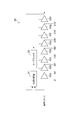
- FIG. 1 is a diagram showing a configuration of an integral AD converter 1 according to an embodiment of the present invention.
- the integrating AD converter 1 includes a comparator 10, a delay adjustment circuit 20, a ripple counter (counter) 30, a TDC (time quantizer) 40, and a DLL (multi-phase clock generator). Circuit) 50 and a Schmitt trigger circuit 60.
- a comparator 10 a comparator 10
- a delay adjustment circuit 20 a ripple counter (counter) 30, a TDC (time quantizer) 40
- a DLL multi-phase clock generator
- the comparator 10 receives a reference voltage ramp having a ramp waveform that changes linearly with respect to time and an analog input voltage vin.
- the comparator 10 compares the reference voltage ramp and the analog input voltage vin and outputs a comparison signal.
- the comparison signal vcomp that is the output of the comparator 10 is at a high level.
- the comparison signal vcomp which is the output of the comparator 10 is inverted at this time t inv and becomes a low level.
- FIG. 2 is a diagram showing a configuration of the delay adjustment circuit 20 in the integral AD converter 1 of the present embodiment.
- the delay adjustment circuit 20 is a circuit that is provided in the subsequent stage of the comparator 10 and outputs the comparison signal with a delay.
- the delay adjustment circuit 20 is a delay line including eight stages of inverters 21a to 21h.
- the delay adjustment circuit 20 delays the comparison signal T output from the comparator 10 by a time dT, and outputs a delayed comparison signal T + dT.
- This time dT is a time of one cycle or more of the main clock signal generated by the DLL 50 described later.
- the number of stages of the inverter 21 is not necessarily eight, and may be any number that can cause a delay of one or more periods of the main clock signal regardless of process variations.
- FIG. 3 is a diagram illustrating a configuration of the ripple counter 30 in the integral AD converter 1 of the present embodiment.
- the ripple counter 30 is a 9-bit ripple counter.
- the ripple counter 30 is configured by connecting nine D-FFs (Flip Flops) 31a to 31i in cascade. Inverted outputs Qb of the D-FFs 31a to 31i (indicated by a line above the character Q in the drawing, the same applies hereinafter) are connected to the data inputs D of the D-FFs 31a to 31i, respectively.
- the inverted outputs Qb of the D-FFs 31a to 31h other than the last stage are also connected to the clock inputs of the D-FFs 31b to 31i of the next stage, respectively.
- the ripple counter 30 operates as follows.
- the output Q and inverted output Qb of the first-stage D-FF 31a change from the high level to the low level or from the low level to the high level, respectively, according to the rising edge of the clock signal CLK input from the TDC 40.
- the output Q and the inverted output Qb of the D-FFs 31b to 31i after the next stage change from the high level to the low level, or from the low level to the high level, respectively, according to the rising of the inverted output of the preceding D-FF 31. . Therefore, the second-stage D-FF 31b changes once every two rises of the clock signal CLK input from the TDC 40, and the third-stage D-FF 31c changes the rise 4 of the clock signal CLK input from the TDC 40. It changes once every time.
- the output Q of each of the D-FFs 31a to 31i outputs a value of 9 bits of a 9-bit count value.
- the order of bit values is such that the output Q of the first-stage D-FF 31a is the least significant bit value, and the output Q of the last-stage D-FF 31i is the most significant bit value.
- FIG. 4 is a diagram showing a configuration of the TDC 40 in the integral AD converter circuit 1 of the present embodiment.
- the TDC 40 includes four D-FFs 41a to 41d, an XOR gate 42, an AND gate 43, a 4-bit counter 44, and an XOR gate 45.
- the TDC 40 is a circuit for measuring the time when the output of the delay adjustment circuit 20 is inverted.
- the D-FF 41a includes two D-latches 411 to 412 and one inverter 413.
- the data input of the D-FF 41 a is connected to the input D of the D-latch 411.
- the output Q of the D-latch 411 is connected to the data input Q of the D-latch 412.
- the clock input of the D-FF 41 a is connected to the clock input of the D-latch 411 and also connected to the input of the inverter 413.
- the output of the inverter 413 is connected to the clock input of the D-latch 412.
- the D-FFs 41b to 41d also have the same configuration as the above-described D-FF 41a.
- a D-latch may be used in place of the D-FFs 41a to 41d.
- the TDC 40 is configured as follows.
- the signal T + dT output from the delay adjustment circuit 20 is input to the clock inputs of the four D-FFs 41a to 41d as the signal Stop.
- four-phase clock signals Clk_deg0, Clk_deg45, Clk_deg90, and Clk_deg135, which are generated in a DLL 50 described later and have a phase difference of 45 degrees, are input to the data inputs of the D-FFs 41a to 41d, respectively.
- the output Q of the D-latch 411 is output as a clock D-latch_clk to the ripple counter 30.
- the inverted output Qb of the D-FF 41a is connected to the first input of the XOR gate 42.
- the outputs Q of the D-FF 41b to D-FF 41d are connected to the second input of the XOR gate 42 through switches controlled by the control signals Address [2] to Address [0], respectively. Further, the reference potential GND is connected to the second input of the XOR gate 42 through a switch controlled by the control signal Address [3]. An output of the XOR gate 42 and a signal Cal described later are input to two inputs of the AND gate 43, respectively. The output of the AND gate 43 is connected to the clock input of the 4-bit counter 44. The 4-bit counter 44 receives the signals Cal and CDS [1] at its input terminals and outputs a 4-bit count value Out [0: 3].
- the two inputs of the XOR circuit 45 are supplied with a comparison signal T output from the comparator 10 and a signal T + dT obtained by delaying the comparison signal T by the delay adjustment circuit 20 and taking an exclusive OR of these signals.
- the signal is output to a power supply line used in the TDC 40. The operation of the TDC 40 will be described in detail later.
- FIG. 5 is a diagram showing a configuration of the DLL 50 in the integral AD converter circuit 1 of the present embodiment.
- the DLL 50 includes a phase comparator 51, a loop filter 52, and eight unit delay circuits 53a to 53h. Eight unit delay circuits 53a to 53h are connected in cascade.
- the phase comparator 51 compares the phase of the reference clock signal input to the DLL 50 with the phase of the clock signal output from the last unit delay circuit 53h, and outputs a signal having a magnitude corresponding to the difference between these phases. Output.
- the loop filter 52 is a filter circuit that smoothes and smoothes the signal output from the phase comparator 51 through a low band.
- the unit delay circuit 53a to the unit delay circuit 53h are configured by, for example, cascading even-numbered inverters, and delay the phase of the input clock.
- Each of the unit delay circuit 53a to unit delay circuit 53h has a delay amount control input for controlling the magnitude of the delay of the clock phase.
- the DLL 50 operates such that the phase difference between the reference clock signal input to the DLL 50 and the signal output from the unit delay circuit 53h is 360 degrees.
- the phase comparator 51 and the loop filter 52 output a signal that reduces the delay amount of the unit delay circuits 53a to 53h and brings the phase difference closer to 360 degrees.
- the phase comparator 51 and the loop filter 52 increase the delay amounts of the unit delay circuits 53a to 53h and output signals that bring the phase difference closer to 360 degrees. And output to the delay amount control inputs of the unit delay circuits 53a to 53h.
- the phase difference between the phase of the reference clock signal and the phase of the output signal of the unit delay circuit 53h is 360 degrees.
- the phase difference between the unit delay circuits 53a to 53h and the reference clock signal is respectively 0 degrees, 45 degrees, 90 degrees, 135 degrees, 180 degrees, 225 degrees, 270 degrees, and 315 degrees.
- four clock outputs of the unit delay circuits 53 a to 53 d are output to the TDC 40.
- the Schmitt trigger circuit 60 is a circuit for shaping the waveform of the clock D-latch_clk output from the TDC 40 and outputting it to the ripple counter 30.
- the operation of the integral AD converter 1 will be described.
- the AD conversion operation when the AD conversion operation is started, the change of the reference voltage ramp is started, and at the same time, the counting operation of the ripple counter 30 is started. Thereafter, when the magnitude relationship between the analog input voltage vin and the reference voltage ramp is reversed, the comparison signal output from the comparator 10 is inverted (see FIG. 12).
- the TDC 40 starts operation at the timing when the comparison signal is inverted.
- time dT from the inversion of the comparison signal the output signal of the delay adjustment circuit 20 is also inverted.
- the TDC 40 stops its operation at the timing when the output signal of the delay adjustment circuit 20 is inverted.
- the ripple counter 30 also stops the counting operation at the timing when the output signal of the delay adjustment circuit 20 is inverted. At this time, the output result of the ripple counter 30 is output to the output out2 of the ripple counter 30, and this output value is the upper bit of the result of AD conversion of the analog input voltage vin.
- TDC 40 The operation of the TDC 40 at the timing when the output signal of the delay adjustment circuit 20 is inverted will be described with reference to FIG. Clocks CLKA, CLKB, CLKC, and CLKD having phases different by 45 degrees are input from the DLL 50 to the TDC 40 as Clk_deg0, Clk_deg45, Clk_deg90, and Clk_deg135, respectively.
- the TDC 40 latches the values of CLKA to CLKD at the timing when the output signal of the delay adjustment circuit 20 is inverted, and sets them as extension codes EB3, EB2, EB1, and EB0, respectively.
- EB3, EB2, EB1, and EB0 are equal to TDC [0], TDC [1], TDC [2], and TDC [3] in FIG.
- the extension codes EB3 to EB0 are latched as 1000.
- the latched value 1000 is decoded as a decode value (extended portion count value) 0 as will be described later. Details of the decoding operation will be described later.
- the extension codes EB3 to EB0 are latched as 1100 and further decoded as the decode value 1.
- CLKA to CLKD are latched and decoded in accordance with the timing at which the output of the delay adjustment circuit 20 is inverted.
- the value of TDC [3] is input to the XOR gate 42, and an exclusive OR with the inverted output Qb of the D-FF 41a is output. Therefore, since the inverted output Qb of the D-FF 41a is 1 when TDC [0] is 0, the XOR gate 42 outputs 1 when TDC [3] is 0. On the other hand, since the inverted output Qb of the D-FF 41a is 0 when TDC [0] is 1, the XOR gate 42 outputs 1 when TDC [3] is 1.
- the AND gate 43 performs an AND operation on the output of the XOR gate 42 and the signal Cal.
- the 4-bit counter 44 counts the number of bits that are 1 out of 3 bits TDC [1] to TDC [3], and TDC [0] When 0] is 1, the number of 0 bits among the 3 bits TDC [1] to TDC [3] is counted.
- the delay adjustment circuit 20 delays the comparison signal output from the comparator 10 by a time equal to or longer than one period of the main clock signal, and the TDC 40
- the operation starts at the timing when the output signal of the comparator 10 is inverted, and stops at the timing when the output signal of the delay adjustment circuit 20 is inverted.
- the TDC 40 can be operated for a required time of at least one cycle of the main clock signal, the power consumption is reduced while improving at least one of the conversion accuracy and the conversion speed of the integral AD converter 1. Can be suppressed.
- the operation time of the ripple counter 30 and the TDC 40 is schematically shown in FIG. FIG.
- the comparison signal output from the comparator can be delayed with a simple configuration.
- the CMOS image sensor 100 includes an integration type AD converter 1, a pixel circuit 70, a row selection circuit 71, a column current source 72, a control signal generation circuit 73, a data buffer 74, and a column selection circuit 75. It is prepared for.
- the pixel circuit 70 is provided in a matrix over a plurality of rows and a plurality of columns.
- One integrating AD converter 1, column current source 72, and data buffer 74 are provided in each column corresponding to each column of the pixel circuit 70.
- the pixel circuit 70 is a circuit for converting the amount of incident light into a voltage and outputting the voltage.
- the row selection circuit 71 is a circuit for selecting one row among the pixel circuits 70 provided over a plurality of rows and causing the pixel circuit 70 in the selected row to output a voltage.
- the analog input voltage vin (see FIG. 1) input to the integral AD converter 1 of each column is the pixel circuit 70 in the row selected by the row selection circuit 71 among the pixel circuits 70 arranged in that column. And the voltage output from the column current source 72.
- the control signal generation circuit 73 is, for example, a circuit for generating a control signal (including a ramp waveform reference voltage ramp (see FIG. 1)) that causes the integrating AD converter 1 to start an AD conversion operation.
- the data buffer 74 is a circuit for holding the lower bit value out1 (see FIG. 1) and the upper bit value out2 (see FIG. 1) output from the integral AD converter 1.
- the pixel circuit 60 in the row selected by the row selection circuit 61 outputs a voltage corresponding to incident light to the integrating AD converter 1.
- the integral AD converter 1 performs an AD conversion operation by the operation as described above, and outputs the digital value of the conversion result to the data buffer 64 at the subsequent stage.
- the data buffer 64 is the digital output from the integral AD converter. Holds the value.
- the column selection circuit 65 sequentially selects the data buffer 64 provided corresponding to each column of the pixel circuit 60, and outputs a value held by the selected data buffer 64.
- the CMOS image sensor 100 includes the integral AD converter 1 that can reduce power consumption while improving at least one of conversion accuracy and conversion speed.
- the operating speed can be improved and the power consumption can be kept low.
- the present invention is not limited to the embodiment described above.
- a PLL Phase locked loop
- a delay line having a phase adjustment circuit may be used as the multiphase clock generation circuit instead of the DLL 50.
- the delay line 55 includes unit delay circuits 56a to 56d and a phase adjustment circuit 57.
- Each of the unit delay circuits 56a to 56d is configured by cascading even-numbered inverters, for example, and delays an input signal by a unit time.
- Each of the unit delay circuits 56a to 56d has an adjustment input for adjusting the delay time between the input and output of the unit delay circuits 56a to 56d by adjusting the driving force.
- the phase adjustment circuit 57 has a START signal input, a STOP signal input, and an adjustment code input.
- the comparison signal T output from the comparator 10 is input to the START signal input.
- the delay comparison signal T + dT output from the delay adjustment circuit 20 is input to the STOP signal input.
- the phase adjustment circuit 57 receives the comparison signal T and the delay comparison signal T + dT, and operates the delay line 55 for the time dT.
- the phase adjustment circuit 57 has an adjustment output for adjusting the delay time of the unit delay circuits 56a to 56d in accordance with the input adjustment code.
- the phase adjustment circuit 57 adjusts the delay time of the unit delay circuits 56a to 56d according to the input of the adjustment code, so that the unit delay circuits 56a, 56b and 56c have a phase relative to the reference clock input to the unit delay circuit 56a. Output clock signals shifted by 45 °, 90 °, and 135 °, respectively.
- a plurality of time quantizers may be provided in the integral type AD converter.
- the timing at which the output signal of the delay adjustment circuit is inverted can be measured more accurately by supplying clock signals having different phases from the multiphase clock generation circuit to the plurality of time quantizers.
- the conversion accuracy of the AD converter can be further improved.
- TDC 40 as a configuration for decoding TDC [0: 3], instead of the configuration using the XOR gate 42, the AND gate 43, and the 4-bit counter 44 of the above-described embodiment, TDC [0: 3] A logic circuit that directly converts ## EQU1 ## to Out [3: 0] may be used.
- various CMOS logic circuits such as a NAND gate having one input fixed can be used as an element for delaying a signal, instead of an inverter.
- the delay adjustment circuit 20 can be configured by cascading even-numbered inverters 21. Further, the delay adjustment circuit 20 may be configured by cascading odd-numbered inverters 21 and using a NOR circuit instead of the XOR circuit 45. Further, the output polarity of the comparator 10 is reversed so that the comparison signal vcomp output from the comparator 10 is inverted from the low level to the high level at the time t inv , and an AND circuit is used in place of the XOR circuit 45. It is good also as a structure.
- the number of bits output from the ripple counter 30 and the TDC 40 is not limited to 9 bits and 3 bits, respectively.
- the number of D-FFs 41 provided in the TDC 40 is increased to eight, and a plurality of phase clocks output from the DLL 50 are set to eight at intervals of 22.5 degrees to obtain a TDC that performs 4-bit output.
- the conversion accuracy or conversion speed of the integral AD converter can be improved by a factor of two.
- the conversion accuracy of the integral AD converter is fixed to 12 bits, the number of bits of the ripple counter 30 can be reduced from 9 bits to 1 bit, and the time required for counting can be halved. The conversion speed is doubled.
- the output of the TDC 40 increases from 3 bits to 4 bits. Therefore, the output of the integral AD converter is combined with the output of the 9-bit ripple counter 30. Increases by 1 bit from 12 bits to 13 bits. That is, the conversion accuracy of the integral AD converter is doubled.
- a circuit simulation was performed on the conversion speed and average power consumption of the integral AD converter described above. This circuit simulation is based on a TSMC 0.18 ⁇ m CMOS process. In addition, both the integral AD converter according to the embodiment and the integral converter according to the comparative example have a 12-bit output.
- Table 1 shows simulation results according to examples of the present invention and comparative examples.
- the integral AD converter according to Embodiment 1 of the present invention includes a 9-bit single slope AD converter (single slope ADC) and a 3-bit TDC.
- the single slope AD converter includes a counter having nine D-FFs as shown in FIG.
- the TDC has a configuration in which each of the four D-FFs 41a to 41d shown in FIG. 4 is replaced with a D-latch.
- the sampling frequency of the integrating AD converter according to Example 1 was 1 MHz, and the average power consumption was 39.9 ⁇ W.
- the two D-latches have the same size as one D-FF obtained by arranging two D-latches.
- the integral AD converter according to Comparative Example 1 includes a 12-bit single slope AD converter, but does not include a TDC.
- the single slope AD converter includes a counter having 12 D-FFs.
- the sampling frequency of the integrating AD converter according to Comparative Example 1 was 125 kHz, and the average power consumption was 39.8 ⁇ W.
- Integral AD converter according to Comparative Example 2 is a conventional single slope AD converter described as background art.
- the integral AD converter according to Comparative Example 2 includes a 9-bit single slope AD converter (single slope ADC) and a 3-bit TDC.
- the single slope AD converter includes a counter having nine D-FFs.
- the TDC includes four D-latches (same size as two D-FFs).
- the sampling frequency of the integrating AD converter according to Comparative Example 2 was 1 MHz, and the average power consumption was 73.9 ⁇ W.
- the sampling frequency is improved by a factor of eight while the power consumption is substantially the same as that of the integrating AD converter according to the first comparative example. Further, in the integrating AD converter according to the first embodiment of the present invention, the sampling frequency is equal as compared with the integrating AD converter according to the comparative example 2, but the power consumption is greatly reduced. This is because in the integral AD converter of the present invention, power consumption at the TDC hardly occurs, and power consumed by the counter occupies most of the power consumption.
- Table 2 shows another embodiment of the present invention and simulation results according to the comparative example.
- Table 2 the data of Comparative Example 1 shown in Table 1 is reprinted for comparison with Examples.
- the integral AD converter according to the second embodiment of the present invention includes an 8-bit single slope AD converter (single slope ADC) and a 4-bit TDC.
- the single slope AD converter includes a counter having 8 D-FFs.
- the TDC has 8 D-latches (same size as 4 D-FFs).
- the sampling frequency of the integrating AD converter according to Example 2 was 2 MHz, and the average power consumption was 40.1 ⁇ W.
- Integral AD converter according to Comparative Example 3 is a conventional single slope AD converter described as background art.
- the integral AD converter according to Comparative Example 3 includes an 8-bit single slope AD converter (single slope ADC) and a 4-bit TDC.
- the single slope AD converter includes a counter having 8 D-FFs.
- the TDC has 8 D-latches (same size as 4 D-FFs).
- the sampling frequency of the integrating AD converter according to Comparative Example 3 was 2 MHz, and the average power consumption was 107.6 ⁇ W.
- the sampling frequency is improved by 16 times while the power consumption is substantially the same as that of the integral AD converter according to the first comparative example. Further, in the integral AD converter according to the second embodiment of the present invention, the sampling frequency is equal to that of the integral AD converter according to the comparative example 3, but the power consumption is greatly reduced.
- the sampling frequency can be improved while the power consumption is substantially equal. That is, the power efficiency is improved by improving the resolution of TDC.
- the resolution of the TDC is improved, the number of D-FFs or D-latches necessary for the TDC is increased, so that the circuit scale is slightly increased.
- the multiphase clock generation circuit further includes any one of a DLL, a PLL having an even-numbered differential ring oscillator, or a delay line having a phase adjustment circuit. It is good as well.
- a DLL digital low-pass filter
- a PLL having an even-numbered differential ring oscillator or a delay line having a phase adjustment circuit. It is good as well.
- a plurality of clock signals latched in a time quantizer are generated. It can be generated with a simple configuration.
- the delay adjustment circuit may be a delay line provided at the subsequent stage of the comparator. According to this configuration, since the delay line is provided in the subsequent stage of the comparator, the comparison signal output from the comparator can be delayed with a simple configuration.
- the integral AD converter according to one aspect of the present invention may include a plurality of time quantizers. According to this configuration, the timing at which the output signal of the delay adjustment circuit is inverted can be measured more accurately by the plurality of time quantizers, so that the conversion accuracy of the integral AD converter can be further improved.
- the integrating AD converter according to one aspect of the present invention may further include a Schmitt trigger circuit that shapes the waveform of the main clock signal and outputs the waveform to the counter. According to this configuration, even when the main clock signal latched by the time quantizer holds an intermediate transition state during rising or falling, the waveform of the main clock signal is shaped by the Schmitt trigger circuit. Malfunctions can be prevented.
- the present invention uses an integration type AD converter circuit and a CMOS image sensor, and can reduce power consumption while improving at least one of conversion accuracy and conversion speed.
Landscapes
- Engineering & Computer Science (AREA)
- Theoretical Computer Science (AREA)
- Physics & Mathematics (AREA)
- General Physics & Mathematics (AREA)
- Analogue/Digital Conversion (AREA)
- Transforming Light Signals Into Electric Signals (AREA)
Abstract
Description


Claims (6)
- 時間に対して線形に変化するランプ波形の参照電圧と入力電圧とを比較して、前記参照電圧と前記入力電圧との比較信号を出力する比較器と、
主クロック信号および前記主クロック信号と位相の異なるクロック信号を含む複数のクロック信号を生成する多相クロック生成回路と、
前記比較器の出力する前記比較信号を、前記主クロック信号の1周期以上の時間だけ遅延させて出力する遅延調整回路と、
前記ランプ波形が変化を始めてから前記遅延調整回路からの出力が反転するまでの時間を前記遅延調整回路が出力する信号および主クロック信号に基づいて計数し、計数した結果を上位ビットとして出力するカウンタと、
前記遅延調整回路の出力信号が反転したタイミングで、前記多相クロック生成回路が生成した複数のクロック信号をラッチし、当該ラッチした値をデコードした結果を下位ビットとして出力する時間量子化器と、
を備え、
前記時間量子化器は、前記比較器の出力する前記比較信号が前記反転したタイミングで動作を開始し、前記遅延調整回路の出力信号が反転したタイミングで前記下位ビットを出力した後に動作を停止する、積分型AD変換装置。 - 前記多相クロック生成回路は、DLL、偶数段の差動リングオシレータを有するPLL、または位相調整回路を有する遅延線のいずれかである、請求項1に記載の積分型AD変換装置。
- 前記遅延調整回路は、前記比較器の後段に設けられる遅延線である、請求項1または2に記載の積分型AD変換装置。
- 前記時間量子化器を複数備える、請求項1~3のいずれか1項に記載の積分型AD変換装置。
- 前記主クロック信号の波形を整形して前記カウンタに出力するシュミットトリガ回路をさらに備える、請求項1~4のいずれか1項に記載の積分型AD変換装置。
- 請求項1~5のいずれか1項に記載の積分型AD変換装置を備えるCMOSイメージセンサ。
Priority Applications (4)
| Application Number | Priority Date | Filing Date | Title |
|---|---|---|---|
| EP13749907.5A EP2816731A4 (en) | 2012-02-17 | 2013-02-15 | INTEGRATED ANALOG DIGITAL TRANSFORMER AND CMOS IMAGE SENSOR |
| KR1020147025397A KR101932794B1 (ko) | 2012-02-17 | 2013-02-15 | 적분형 ad 변환 장치 및 cmos 이미지 센서 |
| JP2013558756A JP6195161B2 (ja) | 2012-02-17 | 2013-02-15 | 積分型ad変換装置およびcmosイメージセンサ |
| US14/379,120 US9571113B2 (en) | 2012-02-17 | 2013-02-15 | Integral A/D converter and CMOS image sensor |
Applications Claiming Priority (2)
| Application Number | Priority Date | Filing Date | Title |
|---|---|---|---|
| JP2012-033196 | 2012-02-17 | ||
| JP2012033196 | 2012-02-17 |
Publications (1)
| Publication Number | Publication Date |
|---|---|
| WO2013122221A1 true WO2013122221A1 (ja) | 2013-08-22 |
Family
ID=48984330
Family Applications (1)
| Application Number | Title | Priority Date | Filing Date |
|---|---|---|---|
| PCT/JP2013/053734 Ceased WO2013122221A1 (ja) | 2012-02-17 | 2013-02-15 | 積分型ad変換装置およびcmosイメージセンサ |
Country Status (5)
| Country | Link |
|---|---|
| US (1) | US9571113B2 (ja) |
| EP (1) | EP2816731A4 (ja) |
| JP (1) | JP6195161B2 (ja) |
| KR (1) | KR101932794B1 (ja) |
| WO (1) | WO2013122221A1 (ja) |
Cited By (12)
| Publication number | Priority date | Publication date | Assignee | Title |
|---|---|---|---|---|
| WO2015037384A1 (ja) * | 2013-09-13 | 2015-03-19 | オリンパス株式会社 | 撮像装置 |
| WO2016027729A1 (ja) * | 2014-08-20 | 2016-02-25 | ソニー株式会社 | 信号処理装置、撮像素子、並びに、電子機器 |
| WO2016075772A1 (ja) * | 2014-11-12 | 2016-05-19 | オリンパス株式会社 | 時間検出回路、ad変換回路、および固体撮像装置 |
| US20160309109A1 (en) * | 2015-04-17 | 2016-10-20 | SK Hynix Inc. | Image sensing device |
| JP2016213549A (ja) * | 2015-04-30 | 2016-12-15 | 国立大学法人北海道大学 | デジタル回路及びA/D(Analog/Digital)変換回路並びにデジタル信号処理方法 |
| WO2017029984A1 (ja) * | 2015-08-19 | 2017-02-23 | 国立大学法人 鹿児島大学 | アナログデジタル変換器 |
| CN108551344A (zh) * | 2018-03-29 | 2018-09-18 | 上海集成电路研发中心有限公司 | 双采样模数转化电路 |
| CN111416619A (zh) * | 2020-03-26 | 2020-07-14 | 中国科学院微电子研究所 | 一种延时测量电路、延时测量方法、电子设备及芯片 |
| CN112770068A (zh) * | 2019-10-21 | 2021-05-07 | 三星电子株式会社 | 模数转换器、图像传感器、及操作模数转换器的方法 |
| KR20210150508A (ko) | 2019-09-26 | 2021-12-10 | 테크 아이디어 컴퍼니 리미티드 | 이미지 센서 |
| WO2022074931A1 (ja) * | 2020-10-06 | 2022-04-14 | ソニーセミコンダクタソリューションズ株式会社 | アナログデジタル変換回路、固体撮像素子、および、アナログデジタル変換回路の制御方法 |
| JP2025019589A (ja) * | 2023-07-28 | 2025-02-07 | 華邦電子股▲ふん▼有限公司 | 制御回路及び半導体記憶装置 |
Families Citing this family (19)
| Publication number | Priority date | Publication date | Assignee | Title |
|---|---|---|---|---|
| KR101932794B1 (ko) * | 2012-02-17 | 2018-12-27 | 국립대학법인 홋가이도 다이가쿠 | 적분형 ad 변환 장치 및 cmos 이미지 센서 |
| TWI648986B (zh) * | 2014-04-15 | 2019-01-21 | Sony Corporation | 攝像元件、電子機器 |
| US9592660B2 (en) * | 2014-12-17 | 2017-03-14 | Arevo Inc. | Heated build platform and system for three dimensional printing methods |
| US9900538B2 (en) * | 2016-05-18 | 2018-02-20 | Semiconductor Components Industries, Llc | Phase delay counting analog-to-digital converter circuitry |
| JP2018014630A (ja) * | 2016-07-21 | 2018-01-25 | ソニーセミコンダクタソリューションズ株式会社 | 固体撮像装置および電子機器 |
| KR102514432B1 (ko) | 2016-09-19 | 2023-03-29 | 에스케이하이닉스 주식회사 | 비교 장치 및 그 동작 방법과 그를 이용한 씨모스 이미지 센서 |
| US10367519B2 (en) * | 2017-10-11 | 2019-07-30 | Tech Idea Co., Ltd. | Time domain A/D converter group and sensor device using the same |
| JP6941890B2 (ja) * | 2017-10-11 | 2021-09-29 | 株式会社テックイデア | 時間領域a/d変換器群およびこれを用いたセンサー装置 |
| JP6987603B2 (ja) * | 2017-10-26 | 2022-01-05 | ブリルニクス シンガポール プライベート リミテッド | 固体撮像装置、固体撮像装置の駆動方法、および電子機器 |
| JP7018293B2 (ja) * | 2017-11-06 | 2022-02-10 | ブリルニクス シンガポール プライベート リミテッド | 固体撮像装置、固体撮像装置の駆動方法、および電子機器 |
| WO2020124518A1 (zh) * | 2018-12-21 | 2020-06-25 | 深圳市汇顶科技股份有限公司 | 模数转换器、图像传感器及手持装置 |
| TWI733415B (zh) * | 2020-04-16 | 2021-07-11 | 瑞昱半導體股份有限公司 | 鎖相迴路裝置與時脈產生方法 |
| JP2021175137A (ja) * | 2020-04-28 | 2021-11-01 | ソニーセミコンダクタソリューションズ株式会社 | 撮像装置 |
| US11947672B2 (en) * | 2021-03-02 | 2024-04-02 | Nxp B.V. | Voltage glitch detection circuit |
| CN113411524B (zh) * | 2021-06-08 | 2022-11-01 | 天津大学 | 应用于图像传感器的低功耗列并行单斜式模数转换器 |
| US11444630B1 (en) * | 2021-06-30 | 2022-09-13 | Novatek Microelectronics Corp. | Column analog-to-digital converter and local counting method thereof |
| TWI788951B (zh) * | 2021-08-13 | 2023-01-01 | 瑞昱半導體股份有限公司 | 類比數位轉換器、低壓差穩壓器及其比較控制電路 |
| US12096149B2 (en) | 2022-02-10 | 2024-09-17 | Samsung Electronics Co., Ltd. | Comparison circuit, and analog-to-digital converter and image sensor including the same |
| CN114726375A (zh) * | 2022-03-09 | 2022-07-08 | 北方广微科技有限公司 | 模数转换器及其控制方法 |
Citations (4)
| Publication number | Priority date | Publication date | Assignee | Title |
|---|---|---|---|---|
| JP2008522258A (ja) * | 2004-11-30 | 2008-06-26 | フリースケール セミコンダクター インコーポレイテッド | 選択的なパワー・ゲーティングを用いて電力消費を低減する装置及び方法 |
| JP2010225738A (ja) * | 2009-03-23 | 2010-10-07 | Yamaha Corp | 半導体集積回路 |
| JP2010258817A (ja) | 2009-04-24 | 2010-11-11 | Sony Corp | 積分型ad変換装置、固体撮像素子、およびカメラシステム |
| JP2011055196A (ja) * | 2009-09-01 | 2011-03-17 | Olympus Corp | Ad変換器および固体撮像装置 |
Family Cites Families (16)
| Publication number | Priority date | Publication date | Assignee | Title |
|---|---|---|---|---|
| US5101206A (en) * | 1989-12-05 | 1992-03-31 | Hewlett-Packard Company | Integrating analog to digital converter |
| US7265594B2 (en) * | 2002-04-03 | 2007-09-04 | Analog Devices, Inc. | Methods and apparatus for generating timing signals |
| US7075353B1 (en) * | 2004-01-05 | 2006-07-11 | National Semiconductor Corporation | Clock generator circuit stabilized over temperature, process and power supply variations |
| US20120244824A1 (en) * | 2007-02-12 | 2012-09-27 | Texas Instruments Incorporated | Minimization of rms phase error in a phase locked loop by dithering of a frequency reference |
| US7671317B2 (en) * | 2007-07-25 | 2010-03-02 | Panasonic Corporation | Physical quantity detecting apparatus and method for driving the same |
| US7863952B2 (en) * | 2008-01-31 | 2011-01-04 | International Business Machines Corporation | Method and circuit for controlling clock frequency of an electronic circuit with noise mitigation |
| US8077069B2 (en) * | 2009-01-20 | 2011-12-13 | Marvell World Trade Ltd. | Two-step subranging ADC architecture |
| JP5493934B2 (ja) | 2010-02-03 | 2014-05-14 | ソニー株式会社 | デューティ補正回路、遅延同期ループ回路、カラムa/d変換器、固体撮像素子およびカメラシステム |
| JP5799531B2 (ja) * | 2010-04-30 | 2015-10-28 | ソニー株式会社 | A/d変換器、a/d変換方法、固体撮像素子およびカメラシステム |
| JP5540901B2 (ja) * | 2010-06-01 | 2014-07-02 | ソニー株式会社 | 積分型a/d変換器、積分型a/d変換方法、固体撮像素子、およびカメラシステム |
| US8618854B2 (en) * | 2010-10-15 | 2013-12-31 | Qualcomm Incorporated | Adaptive clock switching to capture asynchronous data within a phase-to-digital converter |
| JP2012147242A (ja) * | 2011-01-12 | 2012-08-02 | Olympus Corp | 固体撮像装置 |
| US9450596B2 (en) * | 2011-05-09 | 2016-09-20 | Semiconductor Components Industries, Llc | Ramp and successive approximation register analog to digital conversion methods, systems and apparatus |
| KR101932794B1 (ko) * | 2012-02-17 | 2018-12-27 | 국립대학법인 홋가이도 다이가쿠 | 적분형 ad 변환 장치 및 cmos 이미지 센서 |
| US8797194B2 (en) * | 2012-06-20 | 2014-08-05 | The Ohio State University | Phase-based analog-to-digital conversion |
| JP5973321B2 (ja) * | 2012-10-30 | 2016-08-23 | ルネサスエレクトロニクス株式会社 | 固体撮像素子 |
-
2013
- 2013-02-15 KR KR1020147025397A patent/KR101932794B1/ko not_active Expired - Fee Related
- 2013-02-15 JP JP2013558756A patent/JP6195161B2/ja not_active Expired - Fee Related
- 2013-02-15 WO PCT/JP2013/053734 patent/WO2013122221A1/ja not_active Ceased
- 2013-02-15 EP EP13749907.5A patent/EP2816731A4/en not_active Ceased
- 2013-02-15 US US14/379,120 patent/US9571113B2/en not_active Expired - Fee Related
Patent Citations (4)
| Publication number | Priority date | Publication date | Assignee | Title |
|---|---|---|---|---|
| JP2008522258A (ja) * | 2004-11-30 | 2008-06-26 | フリースケール セミコンダクター インコーポレイテッド | 選択的なパワー・ゲーティングを用いて電力消費を低減する装置及び方法 |
| JP2010225738A (ja) * | 2009-03-23 | 2010-10-07 | Yamaha Corp | 半導体集積回路 |
| JP2010258817A (ja) | 2009-04-24 | 2010-11-11 | Sony Corp | 積分型ad変換装置、固体撮像素子、およびカメラシステム |
| JP2011055196A (ja) * | 2009-09-01 | 2011-03-17 | Olympus Corp | Ad変換器および固体撮像装置 |
Non-Patent Citations (2)
| Title |
|---|
| See also references of EP2816731A4 |
| YUKINOBU NLAKIHARA; MHUN SHIN; MASAUKI IKEBE; JUNICHI MOTOHISA; EIICHI SANO: "High-speed ramp-wave generator with interleaved DAC for single-slope AD converter", TECHNICAL REPORT OF INSTITUTE OF IMAGE INFORMATION AND TELEVISION ENGINEERS, vol. 34, no. 29, 23 July 2010 (2010-07-23), pages 89 - 93 |
Cited By (24)
| Publication number | Priority date | Publication date | Assignee | Title |
|---|---|---|---|---|
| JP2015056856A (ja) * | 2013-09-13 | 2015-03-23 | オリンパス株式会社 | 撮像装置 |
| US9204076B2 (en) | 2013-09-13 | 2015-12-01 | Olympus Corporation | Imaging apparatus |
| WO2015037384A1 (ja) * | 2013-09-13 | 2015-03-19 | オリンパス株式会社 | 撮像装置 |
| US10154219B2 (en) | 2014-08-20 | 2018-12-11 | Sony Corporation | Signal processing device, image pickup element, and electronic device |
| WO2016027729A1 (ja) * | 2014-08-20 | 2016-02-25 | ソニー株式会社 | 信号処理装置、撮像素子、並びに、電子機器 |
| JPWO2016027729A1 (ja) * | 2014-08-20 | 2017-06-01 | ソニー株式会社 | 信号処理装置、撮像素子、並びに、電子機器 |
| WO2016075772A1 (ja) * | 2014-11-12 | 2016-05-19 | オリンパス株式会社 | 時間検出回路、ad変換回路、および固体撮像装置 |
| US10609317B2 (en) | 2014-11-12 | 2020-03-31 | Olympus Corporation | Time detection circuit, AD conversion circuit, and solid-state imaging device |
| JPWO2016075772A1 (ja) * | 2014-11-12 | 2017-08-24 | オリンパス株式会社 | 時間検出回路、ad変換回路、および固体撮像装置 |
| US20160309109A1 (en) * | 2015-04-17 | 2016-10-20 | SK Hynix Inc. | Image sensing device |
| US9774809B2 (en) * | 2015-04-17 | 2017-09-26 | SK Hynix Inc. | Image sensing device with analog-dithering scheme |
| JP2016213549A (ja) * | 2015-04-30 | 2016-12-15 | 国立大学法人北海道大学 | デジタル回路及びA/D(Analog/Digital)変換回路並びにデジタル信号処理方法 |
| US10263634B2 (en) | 2015-08-19 | 2019-04-16 | Kagoshima University | Analog-digital converter |
| WO2017029984A1 (ja) * | 2015-08-19 | 2017-02-23 | 国立大学法人 鹿児島大学 | アナログデジタル変換器 |
| CN108551344A (zh) * | 2018-03-29 | 2018-09-18 | 上海集成电路研发中心有限公司 | 双采样模数转化电路 |
| CN108551344B (zh) * | 2018-03-29 | 2022-04-01 | 上海集成电路研发中心有限公司 | 双采样模数转化电路 |
| KR20210150508A (ko) | 2019-09-26 | 2021-12-10 | 테크 아이디어 컴퍼니 리미티드 | 이미지 센서 |
| CN112770068A (zh) * | 2019-10-21 | 2021-05-07 | 三星电子株式会社 | 模数转换器、图像传感器、及操作模数转换器的方法 |
| CN111416619A (zh) * | 2020-03-26 | 2020-07-14 | 中国科学院微电子研究所 | 一种延时测量电路、延时测量方法、电子设备及芯片 |
| CN111416619B (zh) * | 2020-03-26 | 2023-02-03 | 中国科学院微电子研究所 | 一种延时测量电路、延时测量方法、电子设备及芯片 |
| WO2022074931A1 (ja) * | 2020-10-06 | 2022-04-14 | ソニーセミコンダクタソリューションズ株式会社 | アナログデジタル変換回路、固体撮像素子、および、アナログデジタル変換回路の制御方法 |
| US12302022B2 (en) | 2020-10-06 | 2025-05-13 | Sony Semiconductor Solutions Corporation | Analog-to-digital conversion circuit, solid-state image sensor, and method for controlling analog-to-digital conversion circuit |
| JP2025019589A (ja) * | 2023-07-28 | 2025-02-07 | 華邦電子股▲ふん▼有限公司 | 制御回路及び半導体記憶装置 |
| JP7699172B2 (ja) | 2023-07-28 | 2025-06-26 | 華邦電子股▲ふん▼有限公司 | 制御回路及び半導体記憶装置 |
Also Published As
| Publication number | Publication date |
|---|---|
| JPWO2013122221A1 (ja) | 2015-05-18 |
| JP6195161B2 (ja) | 2017-09-13 |
| US9571113B2 (en) | 2017-02-14 |
| KR101932794B1 (ko) | 2018-12-27 |
| KR20140135191A (ko) | 2014-11-25 |
| EP2816731A1 (en) | 2014-12-24 |
| EP2816731A4 (en) | 2015-12-30 |
| US20150014517A1 (en) | 2015-01-15 |
Similar Documents
| Publication | Publication Date | Title |
|---|---|---|
| JP6195161B2 (ja) | 積分型ad変換装置およびcmosイメージセンサ | |
| US9369653B2 (en) | Solid-state imaging apparatus | |
| JP5407685B2 (ja) | 逐次比較型ad変換器及び逐次比較型ad変換器の動作クロック調整方法 | |
| KR101996491B1 (ko) | 이중 데이터 레이트 카운터 및 그를 이용한 아날로그-디지털 변환 장치와 씨모스 이미지 센서 | |
| US10103184B2 (en) | Latch circuit, double data rate ring counter based on the latch circuit, hybrid counting device, analog-digital converting device, and CMOS image sensor | |
| EP3707566B1 (en) | Time-to-digital converter | |
| US11664813B2 (en) | Delay circuit, time to digital converter, and A/D conversion circuit | |
| TWI532323B (zh) | 數位脈波寬度產生器及其產生方法 | |
| JP5525914B2 (ja) | ランプ波生成回路および固体撮像装置 | |
| JP5368194B2 (ja) | 電圧制御遅延発生器およびアナログ・ディジタル変換器 | |
| JP7322482B2 (ja) | 時間デジタル変換器、及びa/d変換回路 | |
| JP7322483B2 (ja) | 時間デジタル変換器、及びa/d変換回路 | |
| CN114787927B (zh) | 基于存储单元环的时间数字转换器 | |
| Lee | A low power two-step cyclic time-to-digital converter without startup time error in 180 nm CMOS | |
| CN120546677A (zh) | 一种异步计数器、斜坡发生器、模数转换器和图像传感器 | |
| JP5234095B2 (ja) | パルス位相差符号化回路 | |
| KR20230099899A (ko) | 다중 클럭을 이용하는 카운터 및 이의 동작 방법 | |
| JP2017079364A (ja) | Pwm信号生成回路 | |
| CN120578031A (zh) | 时间数字转换器及模数转换器、图像传感器 | |
| Gao et al. | A low-jitter multiphase digital delay-locked loop for nuclear instruments and biomedical imaging applications | |
| WO2020045140A1 (ja) | Ad変換器、ad変換器の駆動方法、及び固体撮像装置 |
Legal Events
| Date | Code | Title | Description |
|---|---|---|---|
| 121 | Ep: the epo has been informed by wipo that ep was designated in this application |
Ref document number: 13749907 Country of ref document: EP Kind code of ref document: A1 |
|
| ENP | Entry into the national phase |
Ref document number: 2013558756 Country of ref document: JP Kind code of ref document: A |
|
| WWE | Wipo information: entry into national phase |
Ref document number: 14379120 Country of ref document: US |
|
| NENP | Non-entry into the national phase |
Ref country code: DE |
|
| WWE | Wipo information: entry into national phase |
Ref document number: 2013749907 Country of ref document: EP |
|
| ENP | Entry into the national phase |
Ref document number: 20147025397 Country of ref document: KR Kind code of ref document: A |