WO2013125016A1 - Récepteur de lumière et procédé de réception de lumière - Google Patents
Récepteur de lumière et procédé de réception de lumière Download PDFInfo
- Publication number
- WO2013125016A1 WO2013125016A1 PCT/JP2012/054459 JP2012054459W WO2013125016A1 WO 2013125016 A1 WO2013125016 A1 WO 2013125016A1 JP 2012054459 W JP2012054459 W JP 2012054459W WO 2013125016 A1 WO2013125016 A1 WO 2013125016A1
- Authority
- WO
- WIPO (PCT)
- Prior art keywords
- amplitude
- digital signal
- signal
- synchronization
- optical receiver
- Prior art date
- Legal status (The legal status is an assumption and is not a legal conclusion. Google has not performed a legal analysis and makes no representation as to the accuracy of the status listed.)
- Ceased
Links
Images



Classifications
-
- H—ELECTRICITY
- H04—ELECTRIC COMMUNICATION TECHNIQUE
- H04B—TRANSMISSION
- H04B10/00—Transmission systems employing electromagnetic waves other than radio-waves, e.g. infrared, visible or ultraviolet light, or employing corpuscular radiation, e.g. quantum communication
- H04B10/60—Receivers
- H04B10/61—Coherent receivers
- H04B10/616—Details of the electronic signal processing in coherent optical receivers
-
- A—HUMAN NECESSITIES
- A61—MEDICAL OR VETERINARY SCIENCE; HYGIENE
- A61M—DEVICES FOR INTRODUCING MEDIA INTO, OR ONTO, THE BODY; DEVICES FOR TRANSDUCING BODY MEDIA OR FOR TAKING MEDIA FROM THE BODY; DEVICES FOR PRODUCING OR ENDING SLEEP OR STUPOR
- A61M5/00—Devices for bringing media into the body in a subcutaneous, intra-vascular or intramuscular way; Accessories therefor, e.g. filling or cleaning devices, arm-rests
- A61M5/14—Infusion devices, e.g. infusing by gravity; Blood infusion; Accessories therefor
- A61M5/142—Pressure infusion, e.g. using pumps
- A61M5/145—Pressure infusion, e.g. using pumps using pressurised reservoirs, e.g. pressurised by means of pistons
- A61M5/1452—Pressure infusion, e.g. using pumps using pressurised reservoirs, e.g. pressurised by means of pistons pressurised by means of pistons
- A61M5/1456—Pressure infusion, e.g. using pumps using pressurised reservoirs, e.g. pressurised by means of pistons pressurised by means of pistons with a replaceable reservoir comprising a piston rod to be moved into the reservoir, e.g. the piston rod is part of the removable reservoir
-
- A—HUMAN NECESSITIES
- A61—MEDICAL OR VETERINARY SCIENCE; HYGIENE
- A61M—DEVICES FOR INTRODUCING MEDIA INTO, OR ONTO, THE BODY; DEVICES FOR TRANSDUCING BODY MEDIA OR FOR TAKING MEDIA FROM THE BODY; DEVICES FOR PRODUCING OR ENDING SLEEP OR STUPOR
- A61M5/00—Devices for bringing media into the body in a subcutaneous, intra-vascular or intramuscular way; Accessories therefor, e.g. filling or cleaning devices, arm-rests
- A61M5/14—Infusion devices, e.g. infusing by gravity; Blood infusion; Accessories therefor
- A61M5/142—Pressure infusion, e.g. using pumps
- A61M5/145—Pressure infusion, e.g. using pumps using pressurised reservoirs, e.g. pressurised by means of pistons
- A61M5/1452—Pressure infusion, e.g. using pumps using pressurised reservoirs, e.g. pressurised by means of pistons pressurised by means of pistons
- A61M5/1458—Means for capture of the plunger flange
-
- H—ELECTRICITY
- H04—ELECTRIC COMMUNICATION TECHNIQUE
- H04B—TRANSMISSION
- H04B10/00—Transmission systems employing electromagnetic waves other than radio-waves, e.g. infrared, visible or ultraviolet light, or employing corpuscular radiation, e.g. quantum communication
- H04B10/60—Receivers
- H04B10/66—Non-coherent receivers, e.g. using direct detection
- H04B10/69—Electrical arrangements in the receiver
- H04B10/693—Arrangements for optimizing the preamplifier in the receiver
-
- A—HUMAN NECESSITIES
- A61—MEDICAL OR VETERINARY SCIENCE; HYGIENE
- A61M—DEVICES FOR INTRODUCING MEDIA INTO, OR ONTO, THE BODY; DEVICES FOR TRANSDUCING BODY MEDIA OR FOR TAKING MEDIA FROM THE BODY; DEVICES FOR PRODUCING OR ENDING SLEEP OR STUPOR
- A61M2209/00—Ancillary equipment
- A61M2209/08—Supports for equipment
- A61M2209/082—Mounting brackets, arm supports for equipment
-
- A—HUMAN NECESSITIES
- A61—MEDICAL OR VETERINARY SCIENCE; HYGIENE
- A61M—DEVICES FOR INTRODUCING MEDIA INTO, OR ONTO, THE BODY; DEVICES FOR TRANSDUCING BODY MEDIA OR FOR TAKING MEDIA FROM THE BODY; DEVICES FOR PRODUCING OR ENDING SLEEP OR STUPOR
- A61M2209/00—Ancillary equipment
- A61M2209/08—Supports for equipment
- A61M2209/084—Supporting bases, stands for equipment
Definitions
- the present invention relates to an optical receiver and an optical reception method.
- an optical communication apparatus receives a signal multiplexed in a polarization state orthogonal to the optical transmitter.
- DP-QPSK Double Polarization-Quadrature Phase Shift Keying
- the optical receiver has a local light source (for example, LD: Laser Diode) having substantially the same wavelength as the received signal light, and causes the output light to interfere with the received signal light so that two (X, Y) polarizations are obtained.
- a local light source for example, LD: Laser Diode
- AD Analog / Digital
- the optical coherent transmission by the optical communication apparatus described above has the following problems. That is, the receiver of the optical communication apparatus optimizes the input electric signal within the dynamic range of ADC (Analog Digital Converter) prior to AD conversion, thereby reducing the error rate associated with decoding.
- the receiver reduces the level of the input analog signal at the time of optimization.
- the gain (gain) of the clock component extracted from the input signal in the subsequent digital signal processing circuit is reduced.
- the decrease in the gain of the clock component makes it difficult to establish synchronization, and causes a decoding error in combination with the secular change and the characteristic variation between lanes.
- An increase in error rate at the receiver hinders improvement in optical transmission quality.
- the digital signal processing circuit cannot extract a data component from the digital signal after AD conversion.
- the disclosed technology has been made in view of the above, and an object thereof is to provide an optical receiver and an optical receiving method capable of improving optical transmission quality.
- an optical receiver disclosed in the present application receives coherent light in one aspect.
- the optical receiver includes an amplitude adjustment circuit, a signal processing circuit, and a control circuit.
- the amplitude adjustment circuit adjusts the amplitude of the input signal and outputs it.
- the signal processing circuit inputs a digital signal generated using the analog signal output from the amplitude adjustment circuit, extracts a clock component from the digital signal, and establishes synchronization between the clock component and the data component. Then, the data component is extracted and processed from the digital signal.
- the control circuit sets the amplitude of the analog signal to a first amplitude before establishment of synchronization by the digital signal, and after the establishment of synchronization, the amplitude after the setting is smaller than the first amplitude. Change to the second amplitude.
- optical receiver According to one aspect of the optical receiver disclosed in the present application, there is an effect that the optical transmission quality can be improved.
- FIG. 1 is a diagram illustrating the configuration of the optical receiver according to the embodiment.
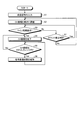
- FIG. 2 is a flowchart for explaining the operation of the optical receiver according to the embodiment.
- FIG. 3 is a diagram illustrating the configuration of the CDR circuit according to the embodiment.
- FIG. 4 is a diagram for explaining the operation of the phase detector according to the embodiment.
- FIG. 5A is a diagram illustrating an example of waveforms of two signals input to the phase detector according to the embodiment.
- FIG. 5B is a diagram illustrating an example of a waveform of a signal output from the phase detector according to the embodiment.
- FIG. 6 is a diagram illustrating the configuration of the digital coherent receiving unit according to the embodiment.
- FIG. 7A is a diagram for explaining a synchronization establishment method when the input amplitude is small.
- FIG. 7B is a diagram for explaining a synchronization establishment method when the input amplitude is large.
- FIG. 8 is a diagram illustrating an example of the gain characteristic of the OA of the optical receiver according to the embodiment.
- FIG. 9 is a diagram illustrating a configuration of an optical receiver according to a modification.
- optical receiver and the optical receiving method disclosed in the present application will be described in detail with reference to the drawings.
- the optical receiver and the optical receiving method disclosed in the present application are not limited by the following embodiments.
- FIG. 1 is a diagram illustrating a configuration of an optical receiver 100 according to an embodiment.
- the optical receiver 100 together with an optical transmitter (not shown), constitutes an optical communication apparatus using the DP-QPSK modulation method being standardized by OIF.
- a 100 Gbps information signal to be transmitted is converted into four 28 Gbps signals in an error correction / encoding circuit and then input to the polarization multiplexed optical modulator.
- the optical transmitter has a wavelength variable light source using a narrow linewidth semiconductor laser as a transmission light source.
- the output light from the transmission light source is separated into two lights inside the polarization multiplexing optical modulator and then input to two QPSK modulators, each having a modulation speed of 28 Gsps (Giga symbol per second).
- each QPSK modulator It is converted into value phase modulated light.
- the signal output from each QPSK modulator is multiplexed and output by the polarization combiner into orthogonal polarization states (S polarization and P polarization).
- S polarization and P polarization orthogonal polarization states
- the transmission speed of the polarization multiplexed signal is 112 Gbps.
- the QPSK modulator a composite optical modulator that orthogonally synthesizes an input electric signal and outputs it can be used.
- the optical receiver 100 includes a polarization separator 101, an X polarization receiver 102, a Y polarization receiver 103, an LD (Laser Diode) 104, a polarization separator 105, and a TIA ( Trans Impedance Amplifier) 106a to 106d and AGC (Automatic Gain Controller) 107a to 107d.
- the optical receiver 100 includes OA (Output Adjuster) 108a to 108d, capacitors 109a to 109d, offset adjusters 110a to 110d, high-speed ADCs 111a to 111d, a digital signal processing circuit 112, and a control circuit 113. Each of these components is connected so that signals and data can be input and output in one direction or in both directions.
- the optical receiver 100 has the LD 104 as a local light source having the same wavelength as the received signal light, and performs coherent detection by causing the output light from the LD 104 to interfere with the received signal light and converting it into an electrical signal. Coherent detection has strong polarization dependence. For this reason, one polarization receiver can receive only an optical signal having the same polarization state as that of the local light. Therefore, the optical receiver 100 is provided with two polarization separators 101 and 105 at a portion where a reception signal is input, and separates the reception signal into two orthogonal polarization components (X component and Y component).
- the optical receiver 100 performs polarization multiplexing of signal light and doubles the amount of information transmission. As a result, it is possible to compensate for a decrease in transmission speed accompanying polarization component separation.
- the polarization separator 101 separates the optical signal P1 input at 112 Gbps into two orthogonal polarization components.
- the X polarization receiver 102 includes an optical 90-degree hybrid 102a and two balanced photodiodes 102b and 102c.
- the optical 90-degree hybrid 102a receives signal light and local light (LD light).
- the optical 90-degree hybrid 102a has a set of output lights P7 and P8 obtained by causing these lights to interfere with each other in the same phase (I) and in the opposite phase (Q), orthogonal (90 degrees, X), and inverse orthogonal ( ⁇ 90). A total of four lights with a set of output lights P9 and P10 interfered with each other at Y degree) are output.
- the latter-stage balanced photodiodes 102b and 102c receive the two sets of output lights P7 to P10 differentially. Accordingly, the balanced photodiodes 102b and 102c can cancel unnecessary DC components from the signal light and the local light, and can efficiently extract only the beat component of each light.
- the balanced photodiodes 102b and 102c convert the received optical signals P7 to P10, which are separated into a total of four components of the X polarization IQ component and the Y polarization IQ component, into electrical signals E1 and E2 (current).
- the Y polarization receiver 103 includes an optical 90-degree hybrid 103a and two balanced photodiodes 103b and 103c.
- the configuration and operation of the Y polarization receiver 103 are the same as the configuration and operation of the X polarization receiver 102 except that the polarization component to be received is the Y component. Therefore, the same reference numerals are used for common components, and detailed description thereof is omitted.
- the TIAs 106a to 106d receive electric signals E1 to E4 output from the balanced photodiodes 102b, 102c, 103b, and 103c, respectively. That is, the TIAs 106a and 106b receive the in-phase interference component (I) of the received optical signals P7 and P8 and the quadrature interference component (Q) of the local light signals P9 and P10 from the two balanced photodiodes 102b and 102c, respectively. To do.
- the TIAs 106c and 106d transmit the in-phase interference component (I) of the received optical signals P11 and P12 and the quadrature interference component (Q) of the local light signals P13 and P14 from the two balanced photodiodes 103b and 103c, respectively. input.
- the TIAs 106a to 106d perform impedance conversion on the input electrical signals E1 to E4, amplify them, and output them as electrical signals E5 to E8.
- the AGCs 107a to 107d control the electrical signals E5 to E8 input from the TIAs 106a to 106d to preset amplitude values.
- the OAs 108a to 108d adjust the amplitudes of the input signals E9 to E12 from the AGCs 107a to 107d and output them.
- the OAs 108a to 108d have four lanes caused by imperfections in the characteristics of the analog portion (such as the X polarization receiver 102, the Y polarization receiver 103, the TIAs 106a to 106d, the AGCs 107a to 107d, and the high speed ADCs 111a to 111d). Signal quality degradation due to variations between them is individually suppressed and normalized.
- the capacitors 109a to 109d are passive elements that store and discharge the electric signals E13 to E16 input from the OAs 108a to 108d, respectively, by electrostatic capacity. Based on an instruction from the control circuit 113, the offset adjusters 110a to 110d give a bias to the high speed signals E17 to E20 that have been DC (Direct Current) cut so that they are within the input range of the high speed ADCs 111a to 111d.
- DC Direct Current
- each signal D1 is AD-converted at high speed, and the signal D1 converted into a digital signal To D4 are output to the subsequent digital signal processing circuit 112.
- the high-speed ADCs 111a to 111d take in the analog signals E21 to E24 at a sampling frequency that is at least twice that of the received signal, convert them to digital signals D1 to D4, and output them to the digital signal processing circuit 112.
- the digital signal processing circuit 112 When the digital signal processing circuit 112 receives the digital signals D1 to D4 output from the high-speed ADCs 111a to 111d, the digital signal processing circuit 112 performs various processes on the digital signals D1 to D4 and performs error correction based on instructions from the control circuit 113. After that, it is output to the outside as a 100 Gbps information signal D5.
- the digital signal processing circuit 112 performs processing such as light source frequency offset compensation, carrier phase estimation, chromatic dispersion compensation, and polarization mode dispersion compensation, for example.
- the control circuit 113 constantly monitors the OAs 108a to 108d for amplitude adjustment and the digital signals D1 to D4 after AD conversion for each lane of a high-speed signal of 28 Gbps or more, and applies feedback control to the OAs 108a to 108d. That is, the control circuit 113 monitors the data after AD conversion by firmware processing, and feeds back the feedback to the OAs 108a to 108d so as to optimize the amplitudes of the input signals E21 to E24 within the dynamic range unique to each of the high speed ADCs 111a to 111d. Take control. As a result, the data component can be extracted in the digital signal processing circuit 112.
- FIG. 2 is a flowchart for explaining the operation of the optical receiver 100 according to the embodiment.
- the control circuit 113 of the optical receiver 100 detects the input of the optical reception signal to the polarization separator 101 with the cancellation of the optical power LOS (Loss Of Signal) (S1), the control circuit 113 sets the value of the signal amplitude in the OAs 108a to 108d. Adjust to a higher value (S2). That is, the control circuit 113 constantly monitors the RMS (Root Mean Square) value after AD conversion, and feedback-controls the signal amplitude value to a higher amplitude value set in advance.
- RMS Root Mean Square
- the higher amplitude value is an amplitude value that enables the digital signal processing circuit 112 to extract clock components necessary for establishing line synchronization from the input signals D1 to D4, and preferably 600 mVpp or more (for example, about 700 mVpp). ).
- the control circuit 113 determines whether line synchronization is established in the high-speed ADCs 111a to 111d based on the feedback control signal F1 (see FIG. 1) input from the high-speed ADCs 111a to 111d via the digital signal processing circuit 112. I do. If the line synchronization is established as a result of the determination (S3; Yes), the control circuit 113 causes the OA 108a to 108d to decrease the amplitude value set higher in S2 by the feedback control signal F2 (see FIG. 1). Instruct (S4).
- the process returns to S4 again.
- the control circuit 113 further reduces the amplitude value.
- the amplitude value lowering process is repeatedly executed until the signal amplitude values in all the OAs 108a to 108d are within the input range (optimized), and ends when the optimization is completed.
- control circuit 113 may individually execute the amplitude value reduction process only for lanes (for example, one) exceeding the input range, or for a plurality of lanes (for example, 2 to 4). May be executed uniformly.
- the amplitude value of the input range is an amplitude value that allows the digital signal processing circuit 112 to extract a data component to be processed from the input signals D1 to D4, and preferably 200 to 600 mVpp (for example, about 300 to 500 mVpp). It is.
- the control circuit 113 sets the amplitude value once set in S2 until the line synchronization is established. Increase gradually. In other words, the control circuit 113 holds in advance an upper limit value (for example, 10 times) of the number of times of increasing the amplitude value as a count value, and gradually increases the amplitude value until the increase number (natural number N times) reaches the count value. (S7). As a result, when line synchronization is established (S3; Yes), the control circuit 113 starts decreasing each value of the signal amplitude in the OAs 108a to 108d (S4).
- an upper limit value for example, 10 times
- control circuit 113 increases the amplitude value until the number of increase of the amplitude value reaches the upper limit count value (S7; Yes) (S7). ; No, S2).
- the control circuit 113 increases the amplitude value with a width of, for example, about 10 to 20 mVpp. Further, the increment per amplitude value need not be constant every time. For example, the control circuit 113 may increase the amplitude value by 20 mVpp for the first five times and increase the amplitude value by 10 mVpp for the subsequent five times.
- the upper limit value which is a determination index for determining whether to increase the amplitude value for establishing synchronization, does not necessarily need to be set by the number of times (for example, 10 times), and may be set based on the amplitude value itself. Good. In this aspect, an upper limit value of, for example, 800 mVpp is set as the count value, and in S7, the current amplitude value is compared with the upper limit value.
- FIG. 3 is a diagram illustrating a configuration of a CDR (Clock Data Recovery) circuit 200 according to the embodiment.
- the CDR circuit 200 includes a buffer 201, a PLL (Phase Locked Loop) circuit 202, and a data decoding circuit (DECoder) 203.
- the PLL circuit 202 includes a phase detector (PD) 202a, an LPF (Low Pass Filter) 202b, and a VCO (Voltage Controlled Oscillator) 202c. Each of these components is connected so as to be able to input and output signals in one direction or in both directions.
- PD phase detector
- LPF Low Pass Filter
- VCO Voltage Controlled Oscillator
- a clock component is included in the transmitted digital signal.
- the CDR circuit 200 has a function of receiving a signal on a transmission line in which a clock component is superimposed on a data component and separating a digital signal into a clock component and a data component, and the digital signal processing circuit of the optical receiver 100 112.
- the CDR circuit 200 extracts clock components from, for example, four serial signals encoded on the transmitter side (FEC (Forward Error Correction) encoding, error correction, etc.). This clock component is used as a sampling clock in the high-speed ADCs 111a to 111d.
- FEC Forward Error Correction
- the receiving-side digital signal processing circuit 112 needs to decode both clock and data components. Therefore, as shown in FIG. 3, the clock component and the data component input to the PLL circuit 202 first pass through the buffer 201 and are branched into two paths.
- the digital signal D6 transmitted through one path is input to the PLL circuit 202 that extracts the clock component, and the digital signal D9 transmitted through the other path is input to the data decoding circuit 203 that generates the data component. Entered.
- the phase detector 202a receives two digital signals D6 and D7 and outputs a digital signal D8 corresponding to the phase difference between these signals. For example, the phase detector 202a generates a digital signal D8 such that the output voltage becomes 0 V when the phase difference between the two input signals D6 and D7 is 90 degrees, and outputs the digital signal D8 to the downstream LPF 202b.
- FIG. 4 is a diagram for explaining the operation of the phase detector 202a according to the embodiment.
- a sine wave digital signal D6 is input to a mixer type phase detector 202a via an RF (Radio Frequency) port.
- the rectangular digital signal D7 is input to the mixer-type phase detector 202a via a LO (Local Oscillator) port.
- the digital signals D6 and D7 having different waveforms are combined and then input to the LPF 202b via an IF (Intermediate Frequency) port as an output signal D8 of the mixer.
- the digital signal D8 becomes a positive DC voltage by the LPF 202b and is output as the digital signal D10.
- FIG. 5A is a diagram illustrating an example of waveforms of two signals input to the phase detector 202a according to the embodiment.
- time unit: second
- input signal voltage unit: V
- the digital signal D6 described above draws a sine wave having an amplitude of 0.5 V and a wavelength of 10 ns
- the digital signal D7 described above is a rectangular wave having the same phase, amplitude, and wavelength as the digital signal D6. Draw. Therefore, when these digital signals D6 and D7 are combined by the phase detector 202a, a waveform as shown in FIG. 5B is generated.
- FIG. 5B is a diagram illustrating an example of waveforms of two signals input to the phase detector 202a according to the embodiment.
- time unit: second
- input signal voltage unit: V
- the digital signal D6 described above draws a sine wave having an amplitude of 0.5 V and a wavelength of 10 ns
- the digital signal D7 described above is a rectangular wave having the same phase, amplitude, and wavelength as the
- FIG. 5B is a diagram illustrating an example of a waveform of a signal output from the phase detector 202a according to the embodiment.
- the digital signal D8 described above when through the LPF202b, high-frequency component is removed, as a digital signal D10 having a positive DC voltage V op, is output from LPF202b.
- the output voltage V op from the LPF 202b becomes a control voltage for the VCO 202c. Therefore, when the amplitude of the digital signal D6 (corresponding to the digital signals D1 to D4 shown in FIG. 1) is small, the voltage V op, that is, the VCO 202c control voltage is also small, and as a result, the clock speed that the VCO 202c can follow is lowered. At the same time, as the amplitude of the digital signal D6 decreases, the value of T r / T f also decreases (gradual inclination), and is easily affected by noise and the like. As a result, jitter performance is degraded.
- the optical receiver 100 increases the amplitude value of the digital signal D6 and increases the value of T r / T f until synchronization is established. This suppresses the influence of noise and the like, and increases the speed at which the VCO 202c can follow. As a result, the clock component can be easily extracted.
- FIG. 6 is a diagram illustrating a configuration of a digital coherent receiving unit according to the embodiment.
- the phase shifter 203c shifts the output clock signal from the VCO 202c, which is established in synchronization by the PLL circuit 202, to four phases (0 °, 90 °, 180 °, 270 °).
- the 4-phase sampler 203b shifts the data input from the buffer 203a to each clock phase shifted by the phase shifter 203c.
- the data shifted to the four phases by the four-phase sampler 203b is AD-converted by the high-speed ADCs 203d-1, 203d-2, 203d-3, and 203d-4, and then converted into a digital signal as an FEC frame synchronization detection circuit 203f. Is output.
- the FEC frame synchronization detection circuit 203f detects the FEC frame preamble pattern (F6, F6, F6, 28, 28) from this digital signal.
- the digital signal processing circuit 203g in the subsequent stage uses the clock closest to the midpoint of the data change point. select. This operation by the digital signal processing circuit 203g is defined as “establishment of synchronization”. With this operation, the XI input signal X1, the XQ input signal X2, the YI input signal Y1, and the YQ input signal Y2 respectively input to the data decoding circuits (DEC) 203, 204, 205, and 206 are converted into the clock component and the data component. After the synchronization is established, it is output to the outside as an XI output signal X3, an XQ output signal X4, a YI output signal Y3, and a YQ output signal Y4.
- DEC data decoding circuits
- FIG. 7A is a diagram for explaining a synchronization establishment method when the input amplitude is small.
- FIG. 7B is a diagram for explaining a synchronization establishment method when the input amplitude is large.
- the phase of the input signal is defined in the x-axis direction (time direction)
- the voltage of the input signal is defined in the y-axis direction.
- the digital signal processing circuit 203g uses 0 ° and 270 ° (dashed lines in FIG. 7A), which are phases close to the data change points Z1 and Z2, as the phase of the data change point. to decide.
- the digital signal processing circuit 203g samples any phase of 90 ° or 180 ° (solid line in FIG. 7A) positioned between them as a clock used for establishing synchronization. For this reason, depending on the wavelength and frequency of the input signal, the optimal phase is not determined, and the clock at the optimal point for establishing synchronization may not always be selected.
- the digital signal processing circuit 203g can accurately select the clock phase that is the optimum point for establishing synchronization from the four phases. That is, the sampling process for establishing synchronization is realized simply and quickly. For the reasons described above, the greater the input amplitude, the easier it is for the optical receiver 100 to extract the clock component from the digital signal, and the establishment of synchronization becomes easier.
- the optical receiver 100 receives coherent light.
- the optical receiver 100 receives coherent light.
- the optical receiver 100 includes OAs 108a to 108d, a digital signal processing circuit 112, and a control circuit 113.
- the OAs 108a to 108d adjust the amplitude of the input signal and output it.
- the digital signal processing circuit 112 inputs a digital signal generated using the analog signals output from the OAs 108a to 108d, extracts a clock component from the digital signal, and establishes synchronization between the clock component and the data component. After that, the data component is extracted and processed from the digital signal.
- the control circuit 113 sets the amplitude of the analog signal to a first amplitude (for example, a large amplitude of about 700 mVpp) before establishment of synchronization by the digital signal, and after establishment of the synchronization, the control circuit 113 sets the amplitude after the setting. Is changed to a second amplitude smaller than the first amplitude (for example, a small amplitude of about 400 mVpp).
- a first amplitude for example, a large amplitude of about 700 mVpp
- the first amplitude is equal to or larger than an amplitude value at which the digital signal processing circuit 112 can establish synchronization between the clock component and the data component using the digital signal.
- the second amplitude is an amplitude within the range in which the digital signal processing circuit 112 can extract the data component from the digital signal (optimized amplitude).
- the control circuit 113 changes the second amplitude to an amplitude within a range having a linearity in the gain characteristic of the amplitude of the output signal with respect to the control voltage applied to the OAs 108a to 108d. It may be limited.
- the optical receiver 100 sets the amplitude to a high value until the synchronization is established with respect to the electrical signal received coherently, and decreases the amplitude according to the input range of the high-speed ADCs 111a to 111d after the synchronization is established. Further, the optical receiver 100 always optimizes the amplitude of the electric signal by performing feedback control of the signal amplitude of each lane after the synchronization is established. More specifically, the optical receiver 100 increases the gain of the input signal until the synchronization is established, and improves the stability of the synchronization establishment. On the other hand, after the synchronization is established, the optical receiver 100 converts the AD converted digital value. By constantly monitoring, feedback control is performed to optimize the gain of the analog input signal within the input dynamic range. At that time, the optical receiver 100 can control the gain adjustment after the synchronization is established so as not to use a non-linear range in which waveform distortion is likely to occur, thereby reducing errors in data decoding and improving signal transmission quality. And
- the optical receiver 100 configures the OAs 108a to 108d separately from the AGCs 107a to 107d.
- the optical receiver 100 is input with the signal variation between the capacitors 109a to 109d and the offset adjusters 110a to 110d being suppressed, compared to the case where the AGC 107a to 107d includes the OA function. It is possible to flexibly and easily cope with fluctuations in optical signals.
- the optimum signal amplitude value at the time of clock extraction is different from the optimum signal amplitude value at the time of data communication.
- the optical receiver can easily extract the clock component by increasing the input signal amplitude and abruptly swinging T r / T f. The line quality in the network is also improved.
- the optical receiver 100 sets the output amplitude value of the optical reception FE (Front End) module to be low so that the signal amplitude is within the input range of the high-speed ADCs 111a to 111d.
- the gain of the clock component extracted from the input signal is lowered.
- the data component and the clock component are not synchronized, or a long time is required until the synchronization is established.
- the amplitude of the input signal to the high-speed ADCs 111a to 111d is increased until the line synchronization is established between the data and the clock by the OAs 108a to 108d and the control circuit 113. Set to a higher value. Then, after establishment of line synchronization, the optical receiver 100 optimizes the amplitude within the ADC dynamic range. As an effect before the line synchronization is established, even if the input signals (sine waves) to the high-speed ADCs 111a to 111d are saturated, the optical receiver 100 increases the input amplitude when the line synchronization of the internal PLL (Phase Locked Loop) is established. Thus, it is possible to increase the gain when extracting the clock component from the input signal. This increases the probability of line synchronization. Furthermore, as an effect after line synchronization is established, the optical receiver 100 can easily extract data components.
- PLL Phase Locked Loop
- the optical receiver 100 can take various feedback control modes.
- some existing optical reception FE modules used in optical coherent transmission include an AGC circuit.
- these optical reception FE modules usually have a large dependence on optical input power.
- Some output amplitudes are not constant.
- the input amplitude to the high-speed ADCs 111a to 111d due to various factors such as fluctuations in optical input power, temperature changes, and aging degradation. May deviate from the optimum range.
- the control circuit 113 of the optical receiver 100 can adopt a feedback control method based on the monitoring result of the RMS value after AD conversion when controlling the amplitude after synchronization is established.
- the control circuit 113 can adopt a feedback control method based on the number of errors in the input signal F1 from the digital signal processing circuit 112. That is, the optical receiver 100 constantly monitors the RMS value or the number of errors in the digital signal processing circuit 112 in the signal communication state after the synchronization is established, so that the output signal E13 from the OAs 108a to 108d is monitored. Always optimize the amplitude of E16 within the ADC dynamic range. This reduces the error rate and improves the signal quality.
- the optical receiver 100 realizes higher transparency by optimizing the input amplitude within the dynamic range of the ADC input and preventing signal deterioration due to waveform distortion.
- the optical receiver 100 uses the control circuit 113 to monitor variations in output data characteristics caused by fluctuations in optical input power, temperature changes, aging degradation, and the like, and feedbacks to the OAs 108a to 108d based on the monitoring results. Apply control. Thereby, the optimal input amplitude is always maintained. As a result, deterioration of the optical signal quality is prevented in advance.
- optical coherent transmission by the optical receiver 100 a total of four electrical signals corresponding to two polarization IQ components are connected to four different lanes connecting the polarization receivers 102 and 103 and the digital signal processing circuit 112. It is divided and transmitted. For this reason, there is a concern that the characteristics between the lanes of the analog portion vary, and this variation is derived from the amplitude variation. Variations in amplitude between lanes cause deterioration in transmission quality. Therefore, the optical receiver 100 is provided with OAs 108a to 108d for all the lanes. Thereby, the control circuit 113 can perform individual feedback control for each of the four lanes when controlling the amplitude after the synchronization is established.
- control circuit 113 can reduce or eliminate variations in characteristics and amplitude that occur between lanes. As a result, the error rate is reduced and the signal quality is improved. That is, the optical receiver 100 individually adjusts the input amplitudes of the four lanes, thereby eliminating variations that occur in the analog portion between the lanes, and performing chromatic dispersion compensation and polarization modes executed by the digital signal processing circuit 112 in the subsequent stage. It is possible to improve transparency in dispersion compensation.
- FIG. 8 is a diagram illustrating an example of gain characteristics of the OAs 108a to 108d of the optical receiver 100 according to the embodiment.
- the voltage applied to each OA 108a to 108d is defined as the OA control voltage (unit is V) on the x axis, and the amplitude of the electric signal output from each OA 108a to 108d is represented on the y axis.
- the value is defined as OA output amplitude (unit: mVpp).
- the value of the OA output amplitude increases as the OA control voltage increases, but the increase width (slope) varies depending on the value of the OA control voltage, and in the course of the increase, the linear range and the non-linear range. And mixed.
- a high-speed operational amplifier for amplitude adjustment has a predetermined output level range, and a non-linear portion in a low control voltage range (eg, 0 to 1.0 V) and a high range (eg, 1.8 V or more).
- a low control voltage range eg, 0 to 1.0 V
- a high range eg, 1.8 V or more.
- the non-linear range R1 exists in a low range where the OA control voltage is V 1 or less
- the non-linear range R3 also exists in a high range where the OA control voltage is V 2 or more.
- a linear range R2 (about 200 to 700 mVpp) of the output amplitude exists when the OA control voltage is between V 1 and V 2 (about 1.0 to 1.8 V).
- the output amplitude value is set to a high value (for example, 700 mVpp or more) for establishing synchronization, the input signal may be clipped (saturated).
- the output amplitude value is set to a low value (for example, 200 mVpp or less) at the time of optimization, there arises a problem that quantization noise increases and signal quality deteriorates. That is, if the amplitude is increased too much, the waveform is distorted, and if it is lowered too much, it is easily affected by noise and the frequency band does not extend.
- the optical receiver 100 considers the gains of analog components such as the OAs 108a to 108d when controlling the amplitude after synchronization is established, and has a good range of OA characteristics (for example, about 200 to It is also possible to adopt a feedback control system that limits the output amplitude value to 700 mVpp (more preferably about 300 to 500 mVpp).
- the control circuit 113 enables the linear range R2 shown in FIG. 8 and the high range of the high-speed ADCs 111a to 111d (the most significant bit (MSB: Most Significant Bit) side) in the signal communication state after synchronization is established.
- the optical receiver 100 can limit the output amplitude value so as not to use the non-linear range of the analog component. As a result, waveform distortion is suppressed and the error rate is reduced. As a result, the optical signal quality is improved.
- the control circuit 113 of the optical receiver 100 monitors the predetermined time (for example, 1 to 100 ⁇ s) without controlling in real time when controlling the amplitude after the synchronization is established in consideration of the stability of the output characteristics of the light. Later, it is possible to adopt a method of performing feedback control collectively based on the monitoring result. As a result, the amount of firm processing by the control circuit 113 is reduced. As a result, the processing load on the optical receiver 100 is reduced.
- FIG. 9 is a diagram illustrating a configuration of an optical receiver 100 according to a modification. As shown in FIG. 9, the configuration of the optical receiver 100 according to the modification is the same as the configuration of the optical receiver 100 shown in FIG. 1 except that the OAs 108a to 108d are not provided. Therefore, the same reference numerals are used for common components, and detailed description thereof is omitted.
- the AGCs 107a to 107d control the electric signals E5 to E8 input from the TIAs 106a to 106d to preset amplitude values, adjust the amplitudes of the electric signals E5 to E8, and output the adjusted electric signals E9 to E12. , And output to the capacitors 109a to 109d in the subsequent stage.
- the amplitudes of the electrical signals E5 to E8 are adjusted by feedback control based on the feedback control signal F2.
- the feedback control described above is implemented by providing the OAs 108a to 108d for amplitude adjustment in each of the four lanes by the optical receiver 100. Therefore, the number of analog circuits is increased. The area also increases. Therefore, in the above modification, the optical receiver 100 performs the same amplitude adjustment as that of the OAs 108a to 108d by the AGCs 107a to 107d instead of the OAs 108a to 108d in the feedback control described above. As a result, the circuit scale is reduced and the mounting area is also reduced. As a result, the optical receiver 100 can be downsized. In addition, power consumption can be reduced.
- one optical receiver 100 may have a plurality of feedback control functions described above. Also, the number of methods to be combined is not limited to two, and any form such as a combination of three or more can be employed. Furthermore, it is of course possible to apply the various feedback control methods described above to the optical receiver 100 according to the modification.
- the optical receiver 100 may individually apply the feedback control function based on the RMS value after AD conversion to four parallel lanes.
- the optical receiver 100 may combine feedback control based on the number of errors and batch feedback control after monitoring for a predetermined time.
- the optical receiver 100 according to the modified example may perform feedback control of a method of limiting the amplitude value of the output signal within a linear range.
Landscapes
- Health & Medical Sciences (AREA)
- Engineering & Computer Science (AREA)
- Physics & Mathematics (AREA)
- Electromagnetism (AREA)
- Computer Networks & Wireless Communication (AREA)
- Signal Processing (AREA)
- Biomedical Technology (AREA)
- Anesthesiology (AREA)
- Vascular Medicine (AREA)
- Heart & Thoracic Surgery (AREA)
- Hematology (AREA)
- Life Sciences & Earth Sciences (AREA)
- Animal Behavior & Ethology (AREA)
- General Health & Medical Sciences (AREA)
- Public Health (AREA)
- Veterinary Medicine (AREA)
- Optical Communication System (AREA)
Abstract
Dans cette invention, un récepteur de lumière (100) reçoit de la lumière cohérente. Ce récepteur de lumière (100) comprend des OA (108a-108d), un circuit de traitement de signal numérique (112) et un circuit de commande (113). Les OA (108a-108d) ajustent l'amplitude d'un signal d'entrée et émettent les résultats. Ledit circuit de traitement de signal numérique (112) entre un signal numérique généré au moyen d'un signal analogique émis par les OA (108a-108d), extrait une composante d'horloge du signal numérique, réalise une synchronisation de la composante d'horloge et d'une composante de données, puis extrait la composante de données du signal numérique et la traite. Avant la réalisation de la synchronisation qui concerne le signal numérique, le circuit de commande (113) définit une première amplitude pour le signal analogique, et, après la réalisation de cette synchronisation, il change ladite amplitude et définit une seconde amplitude inférieure à la première.
Priority Applications (4)
| Application Number | Priority Date | Filing Date | Title |
|---|---|---|---|
| JP2014500823A JP5861765B2 (ja) | 2012-02-23 | 2012-02-23 | 光受信器、及び光受信方法 |
| PCT/JP2012/054459 WO2013125016A1 (fr) | 2012-02-23 | 2012-02-23 | Récepteur de lumière et procédé de réception de lumière |
| CN201280069992.2A CN104137446B (zh) | 2012-02-23 | 2012-02-23 | 光接收器以及光接收方法 |
| US14/444,010 US9344199B2 (en) | 2012-02-23 | 2014-07-28 | Optical receiver and light receiving method |
Applications Claiming Priority (1)
| Application Number | Priority Date | Filing Date | Title |
|---|---|---|---|
| PCT/JP2012/054459 WO2013125016A1 (fr) | 2012-02-23 | 2012-02-23 | Récepteur de lumière et procédé de réception de lumière |
Related Child Applications (1)
| Application Number | Title | Priority Date | Filing Date |
|---|---|---|---|
| US14/444,010 Continuation US9344199B2 (en) | 2012-02-23 | 2014-07-28 | Optical receiver and light receiving method |
Publications (1)
| Publication Number | Publication Date |
|---|---|
| WO2013125016A1 true WO2013125016A1 (fr) | 2013-08-29 |
Family
ID=49005236
Family Applications (1)
| Application Number | Title | Priority Date | Filing Date |
|---|---|---|---|
| PCT/JP2012/054459 Ceased WO2013125016A1 (fr) | 2012-02-23 | 2012-02-23 | Récepteur de lumière et procédé de réception de lumière |
Country Status (4)
| Country | Link |
|---|---|
| US (1) | US9344199B2 (fr) |
| JP (1) | JP5861765B2 (fr) |
| CN (1) | CN104137446B (fr) |
| WO (1) | WO2013125016A1 (fr) |
Cited By (1)
| Publication number | Priority date | Publication date | Assignee | Title |
|---|---|---|---|---|
| JP2016025513A (ja) * | 2014-07-22 | 2016-02-08 | 日本電信電話株式会社 | コヒーレント光受信機 |
Families Citing this family (10)
| Publication number | Priority date | Publication date | Assignee | Title |
|---|---|---|---|---|
| US9225430B2 (en) * | 2013-05-20 | 2015-12-29 | Ciena Corporation | Digital noise loading for optical receivers |
| US9513388B2 (en) * | 2014-03-12 | 2016-12-06 | Sercel | Method for providing synchronization in a data acquisition system |
| US9735886B2 (en) * | 2014-09-02 | 2017-08-15 | Technion Research And Development Foundation Ltd. | Self-coherent robust spectrally efficient optical transmission systems |
| US9806813B2 (en) * | 2014-10-01 | 2017-10-31 | Futurewei Technologies, Inc. | Optical receiver with optical transmitter-specific dispersion post-compensation |
| US10103799B2 (en) * | 2015-03-16 | 2018-10-16 | Lockheed Martin Corporation | Apparatus and method for increased data rates in underwater communications using orbital angular momentum |
| JP6578199B2 (ja) * | 2015-12-16 | 2019-09-18 | 日本ルメンタム株式会社 | 光受信モジュール |
| JP6919291B2 (ja) * | 2017-04-11 | 2021-08-18 | 住友電気工業株式会社 | 光受信器および光受信器の制御方法 |
| JP7608867B2 (ja) * | 2021-02-26 | 2025-01-07 | 富士通株式会社 | 光変調器、光送信器及び光通信装置 |
| US11404596B1 (en) * | 2021-04-20 | 2022-08-02 | Ciena Corporation | Balancing a pair of avalanche photodiodes in a coherent receiver |
| CN115801127A (zh) * | 2021-09-10 | 2023-03-14 | 西安电子科技大学 | 一种低复杂度偏振复用相干RoF链路的方法 |
Citations (4)
| Publication number | Priority date | Publication date | Assignee | Title |
|---|---|---|---|---|
| JP2008278249A (ja) * | 2007-04-27 | 2008-11-13 | Fujitsu Ltd | 光信号受信装置 |
| JP2010080665A (ja) * | 2008-09-26 | 2010-04-08 | Nec Corp | 光受信装置および光受信方法 |
| JP2011035551A (ja) * | 2009-07-30 | 2011-02-17 | Fujitsu Ltd | 光通信装置 |
| WO2011027895A1 (fr) * | 2009-09-07 | 2011-03-10 | 古河電気工業株式会社 | Démodulateur de type plc et système de transmission optique |
Family Cites Families (25)
| Publication number | Priority date | Publication date | Assignee | Title |
|---|---|---|---|---|
| US6707025B2 (en) * | 2002-06-04 | 2004-03-16 | Agilent Technologies, Inc. | High dynamic range receiver |
| US7877019B2 (en) * | 2002-10-16 | 2011-01-25 | Tyco Electronics Subsea Communications Llc | Optical receiver including a system and method of controlling gain of an optical amplifier |
| US7315575B2 (en) * | 2004-03-08 | 2008-01-01 | Nortel Networks Limited | Equalization strategy for dual-polarization optical transport system |
| US7103288B2 (en) * | 2004-03-17 | 2006-09-05 | Nortel Networks Limited | Dynamic control of photodiode bias voltage |
| US7394995B2 (en) * | 2004-04-01 | 2008-07-01 | Avanex Corporation | System and method for a compact optical receiver with wide dynamic range |
| EP1779558B1 (fr) * | 2004-08-12 | 2012-11-28 | Triaccess Technologies, Inc | Detecteur de niveau pour recepteurs optiques |
| US7415213B2 (en) * | 2004-11-24 | 2008-08-19 | Stratalight Communications, Inc. | Optical receiver having transient compensation |
| US7532822B2 (en) * | 2005-02-28 | 2009-05-12 | Nortel Networks Limited | Clock recovery from an optical signal with polarization impairments |
| US7769110B2 (en) * | 2005-05-13 | 2010-08-03 | Broadcom Corporation | Threshold adjust system and method |
| JP4654105B2 (ja) * | 2005-10-11 | 2011-03-16 | 富士通株式会社 | 光受信回路 |
| US7606498B1 (en) * | 2005-10-21 | 2009-10-20 | Nortel Networks Limited | Carrier recovery in a coherent optical receiver |
| JP4399447B2 (ja) | 2006-10-27 | 2010-01-13 | Okiセミコンダクタ株式会社 | Ofdm受信機 |
| CN101552640B (zh) * | 2008-04-01 | 2012-04-11 | 富士通株式会社 | 滤波器系数变更装置和方法 |
| JP2010062639A (ja) * | 2008-09-01 | 2010-03-18 | Canon Inc | 撮像装置 |
| JP5407265B2 (ja) | 2008-10-09 | 2014-02-05 | 富士通株式会社 | 光受信機及び光受信方法 |
| US20100142971A1 (en) * | 2008-12-05 | 2010-06-10 | Sun-Hyok Chang | Apparatus for synchronizing digital signals of coherent optical receiver |
| JP5326584B2 (ja) * | 2009-01-09 | 2013-10-30 | 富士通株式会社 | 遅延処理装置,信号増幅装置,光電変換装置,アナログ/デジタル変換装置,受信装置および受信方法 |
| JP5471099B2 (ja) * | 2009-07-13 | 2014-04-16 | 沖電気工業株式会社 | 加入者端末、光通信ネットワーク及び光通信ネットワークにおける光信号の強度調整方法 |
| WO2012066859A1 (fr) * | 2010-11-18 | 2012-05-24 | 日本電気株式会社 | Dispositif de récepteur optique cohérent et procédé de réception optique cohérente |
| JP5573627B2 (ja) * | 2010-11-22 | 2014-08-20 | 富士通株式会社 | 光デジタルコヒーレント受信器 |
| CN103339882B (zh) * | 2011-02-01 | 2016-05-11 | 日本电气株式会社 | 相干光学接收器,用于检测相干光学接收器中的信道间偏斜的装置和方法 |
| US8942334B1 (en) * | 2011-07-13 | 2015-01-27 | Pmc-Sierra, Inc. | Parallel replica CDR to correct offset and gain in a baud rate sampling phase detector |
| CN104247306B (zh) * | 2012-08-28 | 2017-06-06 | 华为技术有限公司 | 光接收器 |
| CN103713194B (zh) * | 2012-10-08 | 2016-08-03 | 富士通株式会社 | 一种用于时钟恢复的相位检测方法和装置 |
| JP2014187506A (ja) * | 2013-03-22 | 2014-10-02 | Sumitomo Electric Ind Ltd | 光受信器及びその製造方法 |
-
2012
- 2012-02-23 CN CN201280069992.2A patent/CN104137446B/zh not_active Expired - Fee Related
- 2012-02-23 WO PCT/JP2012/054459 patent/WO2013125016A1/fr not_active Ceased
- 2012-02-23 JP JP2014500823A patent/JP5861765B2/ja not_active Expired - Fee Related
-
2014
- 2014-07-28 US US14/444,010 patent/US9344199B2/en not_active Expired - Fee Related
Patent Citations (4)
| Publication number | Priority date | Publication date | Assignee | Title |
|---|---|---|---|---|
| JP2008278249A (ja) * | 2007-04-27 | 2008-11-13 | Fujitsu Ltd | 光信号受信装置 |
| JP2010080665A (ja) * | 2008-09-26 | 2010-04-08 | Nec Corp | 光受信装置および光受信方法 |
| JP2011035551A (ja) * | 2009-07-30 | 2011-02-17 | Fujitsu Ltd | 光通信装置 |
| WO2011027895A1 (fr) * | 2009-09-07 | 2011-03-10 | 古河電気工業株式会社 | Démodulateur de type plc et système de transmission optique |
Cited By (1)
| Publication number | Priority date | Publication date | Assignee | Title |
|---|---|---|---|---|
| JP2016025513A (ja) * | 2014-07-22 | 2016-02-08 | 日本電信電話株式会社 | コヒーレント光受信機 |
Also Published As
| Publication number | Publication date |
|---|---|
| JPWO2013125016A1 (ja) | 2015-05-21 |
| CN104137446B (zh) | 2017-02-22 |
| JP5861765B2 (ja) | 2016-02-16 |
| US20140334831A1 (en) | 2014-11-13 |
| CN104137446A (zh) | 2014-11-05 |
| US9344199B2 (en) | 2016-05-17 |
Similar Documents
| Publication | Publication Date | Title |
|---|---|---|
| JP5861765B2 (ja) | 光受信器、及び光受信方法 | |
| US8483581B2 (en) | Light receiving circuit and signal processing method | |
| US8538279B2 (en) | Method and apparatus for carrier phase estimation and correction in a coherent optical system | |
| US9374172B2 (en) | Optical receiver, optical reception device, and correction method for optical received intensity | |
| US8606118B2 (en) | Optical digital coherent receiver | |
| JP5326584B2 (ja) | 遅延処理装置,信号増幅装置,光電変換装置,アナログ/デジタル変換装置,受信装置および受信方法 | |
| US7747176B2 (en) | Optical receiver | |
| US8886051B2 (en) | Skew compensation and tracking in communications systems | |
| US9509413B2 (en) | Optical receiver, optical receiving device, and method for correcting received optical intensity | |
| JP5460618B2 (ja) | 光学レシーバのための位相制御回路及び方法 | |
| US20140348515A1 (en) | Optical receiver and method for controlling optical receiver | |
| US9083570B2 (en) | Level equalization to compensate for implementation impairments in optical communication systems with high-order modulations | |
| US9871596B2 (en) | Optical receiver and signal processing method | |
| US7711218B2 (en) | Optical reception apparatus and controlling method thereof | |
| US7877019B2 (en) | Optical receiver including a system and method of controlling gain of an optical amplifier | |
| JP7156382B2 (ja) | 光受信装置、通信システム、および受信方法 | |
| EP2418789B1 (fr) | Dispositif optoélectronique pour la photoréception différentielle avec compensation automatique de phase et déséquilibres d'amplitude | |
| US9871597B2 (en) | Apparatus and method for blind LOFO estimation in coherent optical receiver | |
| US20250105582A1 (en) | Integrated optical frequency discriminator |
Legal Events
| Date | Code | Title | Description |
|---|---|---|---|
| 121 | Ep: the epo has been informed by wipo that ep was designated in this application |
Ref document number: 12869571 Country of ref document: EP Kind code of ref document: A1 |
|
| ENP | Entry into the national phase |
Ref document number: 2014500823 Country of ref document: JP Kind code of ref document: A |
|
| NENP | Non-entry into the national phase |
Ref country code: DE |
|
| 122 | Ep: pct application non-entry in european phase |
Ref document number: 12869571 Country of ref document: EP Kind code of ref document: A1 |