WO2013128496A1 - Résonateur à quartz et procédé de fabrication de celui-ci - Google Patents
Résonateur à quartz et procédé de fabrication de celui-ci Download PDFInfo
- Publication number
- WO2013128496A1 WO2013128496A1 PCT/JP2012/001467 JP2012001467W WO2013128496A1 WO 2013128496 A1 WO2013128496 A1 WO 2013128496A1 JP 2012001467 W JP2012001467 W JP 2012001467W WO 2013128496 A1 WO2013128496 A1 WO 2013128496A1
- Authority
- WO
- WIPO (PCT)
- Prior art keywords
- glass plate
- crystal
- plate
- electrode
- crystal resonator
- Prior art date
- Legal status (The legal status is an assumption and is not a legal conclusion. Google has not performed a legal analysis and makes no representation as to the accuracy of the status listed.)
- Ceased
Links
Images





Classifications
-
- H—ELECTRICITY
- H03—ELECTRONIC CIRCUITRY
- H03H—IMPEDANCE NETWORKS, e.g. RESONANT CIRCUITS; RESONATORS
- H03H9/00—Networks comprising electromechanical or electro-acoustic elements; Electromechanical resonators
- H03H9/15—Constructional features of resonators consisting of piezoelectric or electrostrictive material
- H03H9/17—Constructional features of resonators consisting of piezoelectric or electrostrictive material having a single resonator
-
- H—ELECTRICITY
- H03—ELECTRONIC CIRCUITRY
- H03H—IMPEDANCE NETWORKS, e.g. RESONANT CIRCUITS; RESONATORS
- H03H3/00—Apparatus or processes specially adapted for the manufacture of impedance networks, resonating circuits, resonators
- H03H3/007—Apparatus or processes specially adapted for the manufacture of impedance networks, resonating circuits, resonators for the manufacture of electromechanical resonators or networks
- H03H3/02—Apparatus or processes specially adapted for the manufacture of impedance networks, resonating circuits, resonators for the manufacture of electromechanical resonators or networks for the manufacture of piezoelectric or electrostrictive resonators or networks
-
- H—ELECTRICITY
- H03—ELECTRONIC CIRCUITRY
- H03H—IMPEDANCE NETWORKS, e.g. RESONANT CIRCUITS; RESONATORS
- H03H9/00—Networks comprising electromechanical or electro-acoustic elements; Electromechanical resonators
- H03H9/02—Details
- H03H9/05—Holders or supports
- H03H9/10—Mounting in enclosures
- H03H9/1007—Mounting in enclosures for bulk acoustic wave [BAW] devices
- H03H9/1035—Mounting in enclosures for bulk acoustic wave [BAW] devices the enclosure being defined by two sealing substrates sandwiching the piezoelectric layer of the BAW device
-
- H—ELECTRICITY
- H10—SEMICONDUCTOR DEVICES; ELECTRIC SOLID-STATE DEVICES NOT OTHERWISE PROVIDED FOR
- H10N—ELECTRIC SOLID-STATE DEVICES NOT OTHERWISE PROVIDED FOR
- H10N30/00—Piezoelectric or electrostrictive devices
- H10N30/01—Manufacture or treatment
- H10N30/06—Forming electrodes or interconnections, e.g. leads or terminals
-
- H—ELECTRICITY
- H10—SEMICONDUCTOR DEVICES; ELECTRIC SOLID-STATE DEVICES NOT OTHERWISE PROVIDED FOR
- H10N—ELECTRIC SOLID-STATE DEVICES NOT OTHERWISE PROVIDED FOR
- H10N30/00—Piezoelectric or electrostrictive devices
- H10N30/80—Constructional details
- H10N30/87—Electrodes or interconnections, e.g. leads or terminals
- H10N30/875—Further connection or lead arrangements, e.g. flexible wiring boards, terminal pins
-
- H—ELECTRICITY
- H03—ELECTRONIC CIRCUITRY
- H03H—IMPEDANCE NETWORKS, e.g. RESONANT CIRCUITS; RESONATORS
- H03H9/00—Networks comprising electromechanical or electro-acoustic elements; Electromechanical resonators
- H03H9/02—Details
- H03H9/05—Holders or supports
- H03H9/10—Mounting in enclosures
- H03H9/1007—Mounting in enclosures for bulk acoustic wave [BAW] devices
- H03H9/1014—Mounting in enclosures for bulk acoustic wave [BAW] devices the enclosure being defined by a frame built on a substrate and a cap, the frame having no mechanical contact with the BAW device
- H03H9/1021—Mounting in enclosures for bulk acoustic wave [BAW] devices the enclosure being defined by a frame built on a substrate and a cap, the frame having no mechanical contact with the BAW device the BAW device being of the cantilever type
-
- H—ELECTRICITY
- H03—ELECTRONIC CIRCUITRY
- H03H—IMPEDANCE NETWORKS, e.g. RESONANT CIRCUITS; RESONATORS
- H03H9/00—Networks comprising electromechanical or electro-acoustic elements; Electromechanical resonators
- H03H9/15—Constructional features of resonators consisting of piezoelectric or electrostrictive material
- H03H9/21—Crystal tuning forks
-
- Y—GENERAL TAGGING OF NEW TECHNOLOGICAL DEVELOPMENTS; GENERAL TAGGING OF CROSS-SECTIONAL TECHNOLOGIES SPANNING OVER SEVERAL SECTIONS OF THE IPC; TECHNICAL SUBJECTS COVERED BY FORMER USPC CROSS-REFERENCE ART COLLECTIONS [XRACs] AND DIGESTS
- Y10—TECHNICAL SUBJECTS COVERED BY FORMER USPC
- Y10T—TECHNICAL SUBJECTS COVERED BY FORMER US CLASSIFICATION
- Y10T29/00—Metal working
- Y10T29/42—Piezoelectric device making
Definitions
- the present invention relates to a crystal resonator used in an electronic device or the like and a manufacturing method thereof.
- a pair of lids 92 are provided on the upper and lower surfaces of a crystal plate 91 in which a crystal unit piece and a frame are integrally formed.
- a crystal resonator 100 having a structure in which 93 is bonded via bonding films 94, 95, and 96 made of a metal material is known.
- External terminals 98 are formed at the corners from the side surface to the bottom surface of the lower lid 93 of the crystal diaphragm 91. The external terminal 98 electrically connects the electrode pad on the circuit board and the bonding films 95 and 96 on the lower surface of the crystal vibrating plate 91 when the crystal unit 100 is mounted on the circuit board.
- the bonding film 96 on the lower surface of the crystal vibrating plate 91 and the bonding film 94 on the upper surface of the crystal vibrating plate 91 are connected by a through via (not shown), and when a voltage is applied to the electrode pad of the circuit board, the bonding film 94 is connected.
- the bonding film 95 When a voltage difference is generated in the bonding film 95, the crystal vibrating piece formed on the crystal vibrating plate 91 resonates to generate a predetermined frequency.
- a solder paste is applied on a plurality of electrode pads on the circuit board, and a plurality of the electrodes of the electronic component are in contact with the solder paste.
- the electronic components are arranged, the entire circuit board is reflowed, the solder paste is melted all at once, and a plurality of electronic components are collectively fixed to the circuit board.
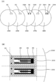
- FIG. 1B is a diagram for explaining a problem that occurs when the crystal resonator 100 is mounted on the circuit board 80.
- the crystal unit 100 is mounted on the circuit board 80, a thin solder 82 is applied on the electrode pads 81 of the circuit board 80 so that the external terminals 98 of the crystal unit 100 are in contact with the solder 82.
- the quartz crystal resonator 100 is placed on the circuit board 80 and the entire circuit board 80 is reflowed.
- the solder 82 melts and spreads over the entire surface of the external terminal 98 of the crystal unit 100.
- the Au component of the external terminal 98 diffuses into the solder 82 to form an Au alloy.
- the melting point of the Au alloy is about 200 ° C., which is lower than the melting point of the lead-free solder, 240 ° C., so-called solder erosion that the Au alloy is absorbed in the solder 82 occurs.
- solder erosion that the Au alloy is absorbed in the solder 82 occurs.
- the molten solder 82 may come into contact with the lower bonding films 95 and 96. This time, the Al component of the lower bonding films 95 and 96 diffuses into the solder 82 to form an Al alloy. Since the melting point of the Al alloy is about 200 ° C., which is lower than the melting point of lead-free solder, 240 ° C., the Al alloy causes solder erosion that is absorbed into the solder 82.
- FIG. 1B shows a state in which the bonding film 95 on the lower surface of the quartz crystal vibrating piece 91 is retracted due to solder erosion at a position indicated by “X” in the drawing.
- the bonding film 95 is not electrically connected to the electrode pad 81, the crystal vibrating piece of the crystal vibrating plate 91 does not vibrate. Since the crystal unit 100 generates a reference clock for operating the circuit, the entire circuit becomes defective.
- the present technology provides a highly reliable crystal resonator and a method for manufacturing the crystal resonator, in which when the crystal resonator is mounted on a circuit board, the electrode of the crystal resonator plate is not melted into solder and connection failure is unlikely to occur. With the goal.
- the first electrode is formed on the lower glass plate on which the first electrode is formed from the side surface to the bottom surface, and provided on the lower glass plate and in contact with the lower glass plate. And a lower glass plate on a side surface on which the electrode of the lower glass plate is formed.
- a projection is provided in parallel with the upper and lower surfaces of the side surface and extending from end to end of the side surface, and the first electrode is provided with a crystal resonator formed on the side surface including the surface of the projection.
- the protrusion is provided on the lower glass plate of the crystal diaphragm, when soldering, it is difficult for the molten solder to contact the electrode of the crystal diaphragm. As a result, there is an effect that solder erosion of the electrode hardly occurs.
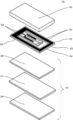
- FIG. 2 is an exploded perspective view of the crystal unit 10 according to the first embodiment.
- the crystal resonator 10 is, for example, bonded to a crystal vibrating plate 20 having a tuning-fork type crystal vibrating piece 26 made of crystal (SiO 2 ) and a first surface of the surface of the crystal vibrating plate 20 to form a crystal.
- the vibrating piece 26 is hermetically sealed in a state where the vibrating piece 26 can vibrate, and the quartz vibrating piece 26 can be vibrated by being bonded to the lid glass 30 serving as a lid of the quartz vibrating plate 20 and the second surface on the back surface of the quartz vibrating plate 20.
- a base glass 32 that is hermetically sealed in a state and serves as a lid of the crystal diaphragm 20.
- a tuning fork type quartz vibrating piece 26 surrounded by an opening is formed at the center of the quartz vibrating plate 20, and an excitation electrode film 28 for vibrating the quartz vibrating piece 26 is formed on the surface thereof.
- An upper bonding film 22 made of the same material as the excitation electrode film 28 and serving as an actual bonding portion with the lid glass 30 is provided on the surface of the frame portion surrounding the quartz vibrating piece 26.
- an excitation electrode film 28 for vibrating the crystal vibrating piece 26 is formed on the surface of the crystal vibrating piece 26 on the back surface of the crystal vibrating plate 20 similarly to the surface.
- lower bonding films 24 and 25 made of the same material as the excitation electrode film and serving as an actual bonding portion with the base glass 32 are provided.
- excitation electrode film 28, the upper bonding film 22, and the lower bonding films 24 and 25 are, for example, an Al layer of 1100 mm formed by sputtering or vacuum deposition.
- the base glass 32 has a three-layer structure of three glass plates made of, for example, soda lime glass or silicon.
- the three glass plates have substantially the same thickness, but the longitudinal length of the second glass plate 37 in the middle is larger than the longitudinal length of the first glass plate 36 thereabove. Further, the length of the middle second glass plate 37 in the longitudinal direction is larger than the length of the third glass plate 38 therebelow in the longitudinal direction.
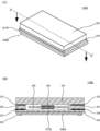
- FIG. 3A is a perspective view of the crystal resonator 10 of this embodiment in which the components shown in the exploded perspective view shown in FIG. 2 are assembled as they are.
- the second glass plate 37 in the middle of the three glass plates on the lower side of the crystal vibration plate 20 is the other first glass plate 36 and the third glass plate. It protrudes from the glass plate 38.
- FIG. 3B is a cross-sectional view of the crystal unit 10 shown in FIG. 3A cut from AA ′ in the direction of the arrow.
- External terminals 40 are formed from the side surfaces of the three glass plates to the bottom surface of the third glass plate 38 at the bottom.
- the external terminal 40 on the left side in the drawing is in contact with the lower bonding film 25 on the lower surface of the crystal diaphragm 20, and the lower bonding film 25 is not shown with the upper bonding film 22 on the upper surface of the crystal diaphragm 20. Connected with through vias. Further, the upper bonding film 22 is electrically connected to the excitation electrode film 28 on the upper surface of the crystal vibrating piece 26.
- the external terminal 40 on the right side in the drawing is in contact with the lower bonding film 24 on the lower surface of the crystal diaphragm 20.
- the lower bonding film 24 is electrically connected to the excitation electrode film 28 on the lower surface of the crystal vibrating piece 26.
- FIG. 4 (A) and 4 (B) show the joint between the electrode pad 81 of the circuit board 80 and the external terminal 40 of the crystal oscillator 10 when the crystal oscillator 10 is mounted on the circuit board 80 from the side.
- FIG. 4 (A) and 4 (B) show the joint between the electrode pad 81 of the circuit board 80 and the external terminal 40 of the crystal oscillator 10 when the crystal oscillator 10 is mounted on the circuit board 80 from the side.
- a thin solder is applied on the electrode pads 81 of the circuit board 80, and the bottom surface of the external terminal 40 of the crystal unit 10 contacts the solder.
- the crystal resonator 10 is arranged so as to do so.
- the solder 82 wets and spreads at the lower part of the protruding part 33, and when the temperature is lowered as it is, the solder 82 is hardened at the lower part of the protruding part 33 as shown in FIG. Even if the external electrode 40 is slightly eroded, the boundary of the lower bonding film 24 of the crystal diaphragm 20 remains unchanged. Next, even if the second reflow is performed, the melted solder 82 does not reach above the protrusion 33, so that the lower bonding film 24 is not eroded.
- the molten solder 82 will be in the depression 34 above the protrusion 33. Since it flows in, it does not contact the lower electrode 24. Even if the external electrode 40 is slightly eroded, the boundary of the lower bonding film 24 of the crystal diaphragm 20 remains unchanged. Next, even if the second reflow is performed, the melted solder 82 remains in the depression 34 above the protrusion 33, and therefore does not reach the lower bonding film 24. I will not wake up.
- the crystal resonator 10 of the present embodiment when soldering to the circuit board 80, the molten solder is melted by the projection 33 on the side surface of the base glass 32 on the mounting side. Therefore, it is possible to provide a highly reliable crystal resonator 10 that is less likely to cause solder erosion of the electrodes.
- the quartz crystal resonator 10 has a five-layer structure as described with reference to the exploded perspective view of FIG.
- Five wafers are prepared: a glass wafer 36W, a second glass wafer 37W as a material for the second glass plate 37, and a third glass wafer 38W as a material for the third glass plate 38.
- the term “wafer” refers to a plate-like material having a size equivalent to that of a semiconductor wafer, and is convenient for manufacturing using a semiconductor device manufacturing apparatus.
- a glass plate having a thickness of 0.4 mm is used as the lid glass wafer 30W.
- a quartz plate having a thickness of 0.13 mm is used for the quartz wafer 20W.
- a glass plate of 0.13 mm is used for each of the first glass wafer 36W, the second glass wafer 37W, and the third glass wafer 38W.
- the constituents of the crystal resonator 10 are formed at the same positions of the lid glass wafer 30W, the crystal wafer 20W, the first glass wafer 36W, the second glass wafer 37W, and the third glass wafer 38W.
- a plurality of crystal diaphragm regions 20S are formed on the crystal wafer 20W.
- an “E” -shaped opening 29 is formed at a substantially central portion in each crystal diaphragm region 20S.
- the portion surrounded by the opening 29 becomes the crystal vibrating piece 26, and the portion surrounding the periphery of the opening 29 becomes a frame-like portion (step S1 in FIG. 7).
- step S2 the upper and lower surfaces of the crystal vibrating piece 26 are etched to make the thickness thinner than the frame-shaped portion.
- a metal film is formed on the surface of the quartz diaphragm piece 26 and the surface of the frame-like portion by sputtering or the like (step S3).
- the material of the metal film is not particularly limited.
- aluminum (Al) and chromium (Cr) are preferably used. In this embodiment, aluminum is used.
- the metal film is then patterned to form the upper bonding film 22 over the entire circumference in the portion corresponding to the excitation electrode film 28 and the surrounding frame-like portion on the crystal vibrating piece 26 (step S4).
- the lower bonding films 24 and 25 are formed over the entire circumference on the portions corresponding to the excitation electrode film 28 and the surrounding frame-like portion on the crystal vibrating piece 26 on the back side of each crystal diaphragm region 20S. Form.
- openings 36H are formed on both sides of first glass wafer 36W forming first glass plate 36 (step S6).
- an opening 38H is formed on both sides of the third glass wafer 38W on which the third glass plate 38 is formed (step S7).
- Step S8 the third glass wafer 38W, the second glass wafer 37W, the first glass wafer 36W, the crystal wafer 20W, and the lid glass wafer 30 are aligned and stacked.
- anodic bonding is performed in an inert gas while applying a voltage to the stacked wafer group (step S9).
- each wafer group is heated to a temperature lower than the softening point of the glass, for example, 100 ° C. to 150 ° C., and a DC voltage of 3 to 5 kV is applied.
- each wafer was heated to about 120 ° C. and a DC voltage of about 3.5 kV was applied.
- the anodically bonded wafer group is diced at the position of the arrow in FIG. 6B, and is singulated as shown in FIG. S10).
- the external electrode 40 having a thickness of 0.63 ⁇ is formed by repeating the sputtering of Cr 600 ⁇ and Au 1500 3 three times so as to be connected to (step S11).
- FIG. 8A is a perspective view of the crystal resonator 10B of the second embodiment.
- FIG. 8B shows a cross-sectional view of the crystal resonator 10B shown in FIG. 8A cut from AA ′ in the direction of the arrow.
- the crystal resonator 10B according to the second embodiment has two glass plates on the lower side of the crystal vibration plate 20. Referring to FIG. 8B, of the two glass plates, the left and right end surfaces of the lower glass plate 38B are recessed from the end surfaces of the upper glass plate 37B. In the drawing, external terminals 40 are formed from the side walls of the two left and right glass plates to the bottom surface of the lower glass 38B.
- the external terminal 40 is formed so as to cover the side surfaces of the lower electrodes 24 and 25 of the crystal diaphragm 20, even if a part of the external terminal 40 is eroded during the first soldering. In the second reflow, the melted solder does not directly touch the lower electrodes 24 and 25 of the crystal vibrating plate 20, and therefore, the highly reliable quartz crystal resonator 10B is less likely to be eroded by the electrode solder. Can be provided.
Landscapes
- Physics & Mathematics (AREA)
- Acoustics & Sound (AREA)
- Engineering & Computer Science (AREA)
- Manufacturing & Machinery (AREA)
- Piezo-Electric Or Mechanical Vibrators, Or Delay Or Filter Circuits (AREA)
Abstract
Lorsqu'un résonateur à quartz est soudé sur une carte de circuits imprimée, si de la soudure en fusion vient en contact avec un film de liaison sur une partie du résonateur à quartz, le film de liaison est absorbé dans la soudure, ce qui entraîne une panne de connexion. La présente invention vise à fournir un résonateur à quartz grâce auquel il est difficile d'avoir un contact entre la soudure en fusion et le film de liaison sur la partie de résonateur à quartz. A cet effet, l'invention concerne un résonateur à quartz (10) comprenant : une plaque de verre inférieure (32) sur laquelle sont formées des premières électrodes (40) s'étendant entre les surfaces latérales de celle-ci et la surface inférieure de celle-ci; une plaque de cristal (20) qui est placée au-dessus de la plaque de verre inférieure (32), et qui a des secondes électrodes (24, 25) formées sur une surface de celle-ci venant en butée contre la plaque de verre inférieure (32), lesdites électrodes étant connectées aux premières électrodes (40); et une plaque de verre supérieure (30) placée au-dessus de la plaque de cristal (20). Des parties en saillie (33) sont placées sur les surfaces latérales de la plaque de verre inférieure (32) ayant des électrodes formées sur celles-ci, lesdites parties en saillie étant parallèles aux surfaces verticales de la plaque de verre inférieure (32) et s'étendant entre les extrémités des surfaces latérales et les extrémités de celles-ci. Les premières électrodes (40) sont formées sur les surfaces latérales, ce qui comprend les surfaces des parties en saillie (33).
Priority Applications (3)
| Application Number | Priority Date | Filing Date | Title |
|---|---|---|---|
| JP2014501828A JP5854123B2 (ja) | 2012-03-02 | 2012-03-02 | 水晶振動子及びその製造方法 |
| PCT/JP2012/001467 WO2013128496A1 (fr) | 2012-03-02 | 2012-03-02 | Résonateur à quartz et procédé de fabrication de celui-ci |
| US14/465,221 US9853627B2 (en) | 2012-03-02 | 2014-08-21 | Crystal resonator, and production method therefor |
Applications Claiming Priority (1)
| Application Number | Priority Date | Filing Date | Title |
|---|---|---|---|
| PCT/JP2012/001467 WO2013128496A1 (fr) | 2012-03-02 | 2012-03-02 | Résonateur à quartz et procédé de fabrication de celui-ci |
Related Child Applications (1)
| Application Number | Title | Priority Date | Filing Date |
|---|---|---|---|
| US14/465,221 Continuation US9853627B2 (en) | 2012-03-02 | 2014-08-21 | Crystal resonator, and production method therefor |
Publications (1)
| Publication Number | Publication Date |
|---|---|
| WO2013128496A1 true WO2013128496A1 (fr) | 2013-09-06 |
Family
ID=49081762
Family Applications (1)
| Application Number | Title | Priority Date | Filing Date |
|---|---|---|---|
| PCT/JP2012/001467 Ceased WO2013128496A1 (fr) | 2012-03-02 | 2012-03-02 | Résonateur à quartz et procédé de fabrication de celui-ci |
Country Status (3)
| Country | Link |
|---|---|
| US (1) | US9853627B2 (fr) |
| JP (1) | JP5854123B2 (fr) |
| WO (1) | WO2013128496A1 (fr) |
Cited By (1)
| Publication number | Priority date | Publication date | Assignee | Title |
|---|---|---|---|---|
| EP3086471A4 (fr) * | 2013-12-20 | 2017-04-12 | Daishinku Corporation | Dispositif d'oscillation piézoélectrique |
Families Citing this family (2)
| Publication number | Priority date | Publication date | Assignee | Title |
|---|---|---|---|---|
| GB201610886D0 (en) * | 2016-06-22 | 2016-08-03 | Element Six Tech Ltd | Bonding of diamond wafers to carrier substrates |
| CN121690105B (zh) * | 2026-02-10 | 2026-04-28 | 成都晶宝时频技术股份有限公司 | 一种晶体谐振器的无调频制备方法 |
Citations (12)
| Publication number | Priority date | Publication date | Assignee | Title |
|---|---|---|---|---|
| JPS51103358U (fr) * | 1975-02-17 | 1976-08-19 | ||
| JP2000286671A (ja) * | 1999-01-29 | 2000-10-13 | Seiko Instruments Inc | 圧電振動子 |
| JP2002121037A (ja) * | 2000-08-07 | 2002-04-23 | Nippon Sheet Glass Co Ltd | 電子部品パッケージ用多数個取りガラス板の製造方法 |
| JP2003110397A (ja) * | 2001-09-26 | 2003-04-11 | Murata Mfg Co Ltd | 表面実装型電子部品 |
| JP2003318690A (ja) * | 2002-04-22 | 2003-11-07 | Nippon Dempa Kogyo Co Ltd | 表面実装用の水晶振動子 |
| JP2006033265A (ja) * | 2004-07-14 | 2006-02-02 | Seiko Epson Corp | 圧電デバイスの製造方法 |
| JP2009135574A (ja) * | 2007-11-28 | 2009-06-18 | Nippon Dempa Kogyo Co Ltd | 表面実装用の水晶発振器 |
| JP2010004455A (ja) * | 2008-06-23 | 2010-01-07 | Nippon Dempa Kogyo Co Ltd | 圧電デバイスとその製造方法 |
| JP2010087573A (ja) * | 2008-09-29 | 2010-04-15 | Nippon Dempa Kogyo Co Ltd | 圧電デバイスとその製造方法 |
| JP2010093675A (ja) * | 2008-10-10 | 2010-04-22 | Epson Toyocom Corp | 圧電振動子 |
| WO2010114115A1 (fr) * | 2009-04-03 | 2010-10-07 | 株式会社大真空 | Ensemble d'éléments de boîtier, procédé de fabrication de l'ensemble d'éléments de boîtier, élément de boîtier, et procédé de fabrication de dispositif vibrant piézoélectrique utilisant l'élément de boîtier |
| JP2011155338A (ja) * | 2010-01-26 | 2011-08-11 | Seiko Epson Corp | 圧電振動子 |
Family Cites Families (8)
| Publication number | Priority date | Publication date | Assignee | Title |
|---|---|---|---|---|
| US3773684A (en) * | 1964-06-29 | 1973-11-20 | A Marks | Dipolar electro-optic compositions and method of preparation |
| DE69106240T2 (de) * | 1990-07-02 | 1995-05-11 | Seiko Epson Corp | Mikropumpe und Verfahren zur Herstellung einer Mikropumpe. |
| JP2786321B2 (ja) * | 1990-09-07 | 1998-08-13 | 株式会社日立製作所 | 半導体容量式加速度センサ及びその製造方法 |
| JP2776142B2 (ja) * | 1992-05-15 | 1998-07-16 | 株式会社日立製作所 | 加速度センサ |
| US5647932A (en) * | 1993-05-18 | 1997-07-15 | Matsushita Electric Industrial Co., Ltd. | Method of processing a piezoelectric device |
| US6670024B1 (en) * | 2002-06-05 | 2003-12-30 | The Regents Of The University Of California | Glass-silicon column |
| KR100821413B1 (ko) * | 2004-03-23 | 2008-04-11 | 가시오게산키 가부시키가이샤 | 적층구조 및 그 제조방법 |
| JP5054146B2 (ja) | 2010-02-01 | 2012-10-24 | 日本電波工業株式会社 | 圧電デバイス及びその製造方法 |
-
2012
- 2012-03-02 JP JP2014501828A patent/JP5854123B2/ja not_active Expired - Fee Related
- 2012-03-02 WO PCT/JP2012/001467 patent/WO2013128496A1/fr not_active Ceased
-
2014
- 2014-08-21 US US14/465,221 patent/US9853627B2/en not_active Expired - Fee Related
Patent Citations (12)
| Publication number | Priority date | Publication date | Assignee | Title |
|---|---|---|---|---|
| JPS51103358U (fr) * | 1975-02-17 | 1976-08-19 | ||
| JP2000286671A (ja) * | 1999-01-29 | 2000-10-13 | Seiko Instruments Inc | 圧電振動子 |
| JP2002121037A (ja) * | 2000-08-07 | 2002-04-23 | Nippon Sheet Glass Co Ltd | 電子部品パッケージ用多数個取りガラス板の製造方法 |
| JP2003110397A (ja) * | 2001-09-26 | 2003-04-11 | Murata Mfg Co Ltd | 表面実装型電子部品 |
| JP2003318690A (ja) * | 2002-04-22 | 2003-11-07 | Nippon Dempa Kogyo Co Ltd | 表面実装用の水晶振動子 |
| JP2006033265A (ja) * | 2004-07-14 | 2006-02-02 | Seiko Epson Corp | 圧電デバイスの製造方法 |
| JP2009135574A (ja) * | 2007-11-28 | 2009-06-18 | Nippon Dempa Kogyo Co Ltd | 表面実装用の水晶発振器 |
| JP2010004455A (ja) * | 2008-06-23 | 2010-01-07 | Nippon Dempa Kogyo Co Ltd | 圧電デバイスとその製造方法 |
| JP2010087573A (ja) * | 2008-09-29 | 2010-04-15 | Nippon Dempa Kogyo Co Ltd | 圧電デバイスとその製造方法 |
| JP2010093675A (ja) * | 2008-10-10 | 2010-04-22 | Epson Toyocom Corp | 圧電振動子 |
| WO2010114115A1 (fr) * | 2009-04-03 | 2010-10-07 | 株式会社大真空 | Ensemble d'éléments de boîtier, procédé de fabrication de l'ensemble d'éléments de boîtier, élément de boîtier, et procédé de fabrication de dispositif vibrant piézoélectrique utilisant l'élément de boîtier |
| JP2011155338A (ja) * | 2010-01-26 | 2011-08-11 | Seiko Epson Corp | 圧電振動子 |
Cited By (2)
| Publication number | Priority date | Publication date | Assignee | Title |
|---|---|---|---|---|
| EP3086471A4 (fr) * | 2013-12-20 | 2017-04-12 | Daishinku Corporation | Dispositif d'oscillation piézoélectrique |
| US10630255B2 (en) | 2013-12-20 | 2020-04-21 | Daishinku Corporation | Piezoelectric resonator device |
Also Published As
| Publication number | Publication date |
|---|---|
| US20140361666A1 (en) | 2014-12-11 |
| US9853627B2 (en) | 2017-12-26 |
| JP5854123B2 (ja) | 2016-02-09 |
| JPWO2013128496A1 (ja) | 2015-07-30 |
Similar Documents
| Publication | Publication Date | Title |
|---|---|---|
| JP3989663B2 (ja) | 圧電振動子と圧電振動子の製造方法 | |
| JP3887137B2 (ja) | 圧電振動子の製造方法 | |
| JP2002319838A (ja) | 圧電デバイス及びそのパッケージ | |
| CN101399527A (zh) | 压电装置及压电装置的制造方法 | |
| JP2015128276A (ja) | 表面実装水晶振動子及びその製造方法 | |
| WO2011010521A1 (fr) | Oscillateur à quartz monté en surface | |
| JP4292825B2 (ja) | 水晶振動片の製造方法 | |
| CN102714489B (zh) | 电子器件封装体用密封部件、电子器件封装体、以及电子器件封装体用密封部件的制造方法 | |
| CN114208027A (zh) | 压电振动板、压电振动器件以及压电振动器件的制造方法 | |
| JP5550373B2 (ja) | パッケージの製造方法 | |
| JP5398689B2 (ja) | 圧電デバイス及びその製造方法 | |
| JP4978030B2 (ja) | 圧電デバイス | |
| JP2012217111A (ja) | 圧電デバイス及びその製造方法 | |
| JP5854123B2 (ja) | 水晶振動子及びその製造方法 | |
| JP5251224B2 (ja) | 圧電振動デバイスの製造方法および圧電振動デバイス | |
| US8624470B2 (en) | Piezoelectric devices including electrode-less vibrating portions | |
| JP2013051560A (ja) | 圧電デバイス | |
| JP5171210B2 (ja) | 圧電振動子の製造方法 | |
| JP5498677B2 (ja) | 水晶発振子の製造方法 | |
| JP2012257180A (ja) | 圧電デバイスの製造方法及び圧電デバイス | |
| JP2009135749A (ja) | 圧電振動子及び圧電発振器 | |
| JP2018125579A (ja) | 音叉型水晶素子及び音叉型水晶素子が実装された水晶デバイス並びに音叉型水晶素子の製造方法 | |
| JP2012195918A (ja) | 圧電デバイス | |
| JP2011151857A (ja) | 圧電振動子、電子デバイス及び電子機器 | |
| JP5915179B2 (ja) | 電子デバイス、発振器、電子デバイスの製造方法、及び発振器の製造方法 |
Legal Events
| Date | Code | Title | Description |
|---|---|---|---|
| 121 | Ep: the epo has been informed by wipo that ep was designated in this application |
Ref document number: 12869821 Country of ref document: EP Kind code of ref document: A1 |
|
| ENP | Entry into the national phase |
Ref document number: 2014501828 Country of ref document: JP Kind code of ref document: A |
|
| NENP | Non-entry into the national phase |
Ref country code: DE |
|
| 122 | Ep: pct application non-entry in european phase |
Ref document number: 12869821 Country of ref document: EP Kind code of ref document: A1 |