WO2013128578A1 - Appareil de commande et procédé de commande d'un appareil de commande - Google Patents
Appareil de commande et procédé de commande d'un appareil de commande Download PDFInfo
- Publication number
- WO2013128578A1 WO2013128578A1 PCT/JP2012/054969 JP2012054969W WO2013128578A1 WO 2013128578 A1 WO2013128578 A1 WO 2013128578A1 JP 2012054969 W JP2012054969 W JP 2012054969W WO 2013128578 A1 WO2013128578 A1 WO 2013128578A1
- Authority
- WO
- WIPO (PCT)
- Prior art keywords
- signal processing
- processing module
- configuration
- volatile memory
- module
- Prior art date
- Legal status (The legal status is an assumption and is not a legal conclusion. Google has not performed a legal analysis and makes no representation as to the accuracy of the status listed.)
- Ceased
Links
Images




Classifications
-
- G—PHYSICS
- G06—COMPUTING OR CALCULATING; COUNTING
- G06F—ELECTRIC DIGITAL DATA PROCESSING
- G06F3/00—Input arrangements for transferring data to be processed into a form capable of being handled by the computer; Output arrangements for transferring data from processing unit to output unit, e.g. interface arrangements
- G06F3/06—Digital input from, or digital output to, record carriers, e.g. RAID, emulated record carriers or networked record carriers
- G06F3/0601—Interfaces specially adapted for storage systems
- G06F3/0628—Interfaces specially adapted for storage systems making use of a particular technique
- G06F3/0629—Configuration or reconfiguration of storage systems
-
- G—PHYSICS
- G06—COMPUTING OR CALCULATING; COUNTING
- G06F—ELECTRIC DIGITAL DATA PROCESSING
- G06F15/00—Digital computers in general; Data processing equipment in general
- G06F15/76—Architectures of general purpose stored program computers
- G06F15/78—Architectures of general purpose stored program computers comprising a single central processing unit
- G06F15/7867—Architectures of general purpose stored program computers comprising a single central processing unit with reconfigurable architecture
-
- G—PHYSICS
- G05—CONTROLLING; REGULATING
- G05B—CONTROL OR REGULATING SYSTEMS IN GENERAL; FUNCTIONAL ELEMENTS OF SUCH SYSTEMS; MONITORING OR TESTING ARRANGEMENTS FOR SUCH SYSTEMS OR ELEMENTS
- G05B15/00—Systems controlled by a computer
- G05B15/02—Systems controlled by a computer electric
-
- G—PHYSICS
- G06—COMPUTING OR CALCULATING; COUNTING
- G06F—ELECTRIC DIGITAL DATA PROCESSING
- G06F11/00—Error detection; Error correction; Monitoring
-
- G—PHYSICS
- G06—COMPUTING OR CALCULATING; COUNTING
- G06F—ELECTRIC DIGITAL DATA PROCESSING
- G06F11/00—Error detection; Error correction; Monitoring
- G06F11/22—Detection or location of defective computer hardware by testing during standby operation or during idle time, e.g. start-up testing
- G06F11/2289—Detection or location of defective computer hardware by testing during standby operation or during idle time, e.g. start-up testing by configuration test
-
- G—PHYSICS
- G06—COMPUTING OR CALCULATING; COUNTING
- G06F—ELECTRIC DIGITAL DATA PROCESSING
- G06F3/00—Input arrangements for transferring data to be processed into a form capable of being handled by the computer; Output arrangements for transferring data from processing unit to output unit, e.g. interface arrangements
- G06F3/06—Digital input from, or digital output to, record carriers, e.g. RAID, emulated record carriers or networked record carriers
- G06F3/0601—Interfaces specially adapted for storage systems
- G06F3/0602—Interfaces specially adapted for storage systems specifically adapted to achieve a particular effect
- G06F3/0604—Improving or facilitating administration, e.g. storage management
-
- G—PHYSICS
- G06—COMPUTING OR CALCULATING; COUNTING
- G06F—ELECTRIC DIGITAL DATA PROCESSING
- G06F3/00—Input arrangements for transferring data to be processed into a form capable of being handled by the computer; Output arrangements for transferring data from processing unit to output unit, e.g. interface arrangements
- G06F3/06—Digital input from, or digital output to, record carriers, e.g. RAID, emulated record carriers or networked record carriers
- G06F3/0601—Interfaces specially adapted for storage systems
- G06F3/0668—Interfaces specially adapted for storage systems adopting a particular infrastructure
- G06F3/0671—In-line storage system
- G06F3/0683—Plurality of storage devices
-
- H—ELECTRICITY
- H03—ELECTRONIC CIRCUITRY
- H03K—PULSE TECHNIQUE
- H03K19/00—Logic circuits, i.e. having at least two inputs acting on one output; Inverting circuits
- H03K19/02—Logic circuits, i.e. having at least two inputs acting on one output; Inverting circuits using specified components
- H03K19/173—Logic circuits, i.e. having at least two inputs acting on one output; Inverting circuits using specified components using elementary logic circuits as components
-
- H—ELECTRICITY
- H03—ELECTRONIC CIRCUITRY
- H03K—PULSE TECHNIQUE
- H03K19/00—Logic circuits, i.e. having at least two inputs acting on one output; Inverting circuits
- H03K19/02—Logic circuits, i.e. having at least two inputs acting on one output; Inverting circuits using specified components
- H03K19/173—Logic circuits, i.e. having at least two inputs acting on one output; Inverting circuits using specified components using elementary logic circuits as components
- H03K19/177—Logic circuits, i.e. having at least two inputs acting on one output; Inverting circuits using specified components using elementary logic circuits as components arranged in matrix form
- H03K19/17748—Structural details of configuration resources
- H03K19/1776—Structural details of configuration resources for memories
Definitions
- the present invention relates to a control device and a control device setting method, and more particularly to a control device including a signal processing module including a field programmable gate array and a control method of the control device.
- control device including a signal processing module including a field programmable gate array is known.
- a control device is disclosed in, for example, Japanese Patent Laid-Open No. 2000-105759.
- JP-A-2000-105759 discloses an FPGA (Field Programmable Gate Array) and a non-volatile PROM (logic information (configuration information) for programming the FPGA as a CPU core (arithmetic processing unit)).
- An integrated circuit with a programmable read-only memory is disclosed. Such an integrated circuit is used for a signal processing module of a control device. In general, programming an FPGA as a circuit having a desired function is called configuration.
- the present invention has been made to solve the above-described problems, and an object of the present invention is to provide a control device and a control method for the control device that can reduce the size of the device. It is.
- a control device includes a signal processing module including a field programmable gate array and a volatile memory in which configuration information of the field programmable gate array is stored.
- the volatile memory is configured to be accessible.
- the signal processing module of the control device is provided with a volatile memory in which configuration information of the field programmable gate array is stored, and the field programmable gate array is configured after the configuration. Also configured to be accessible to volatile memory.
- the volatile memory in which the configuration information of the field programmable gate array is stored can be used as a memory for storing various data used when the field programmable gate array after the configuration is operated. .
- a control method of a control device is a control method of a control device including a control module and a signal processing module including a field programmable gate array and a volatile memory, and configuration information of the field programmable gate array
- the field programmable gate array functions as an arithmetic processing unit of the signal processing module by acquiring from the control module and storing it in the volatile memory and performing configuration based on the configuration information stored in the volatile memory. And a step of allowing the arithmetic processing unit to access the volatile memory and performing arithmetic processing by the arithmetic processing unit.
- the field programmable gate array is connected to the signal processing module.
- the volatile memory storing the configuration information of the field programmable gate array can be used as a memory for storing various data used when the field programmable gate array after the configuration operates as the arithmetic processing unit. Can be used.
- a memory for storing various data used when the field programmable gate array after configuration operates as an arithmetic processing unit is separated from a memory for storing configuration information of the field programmable gate array. Since it is not necessary to provide the control device, it is possible to provide a control method for the control device that can reduce the size of the device.
- the device can be downsized.
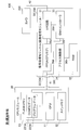
- the PLC 100 is an example of a “control device”.
- the PLC 100 includes a power module 10 for supplying power to the entire PLC 100, a CPU module 20 for controlling the entire PLC 100, and a plurality of power modules 10 and a plurality of CPU modules 20 connected to the CPU module 20. And a signal processing module 30.
- the CPU module 20 is an example of a “control module”.
- Each of the plurality of signal processing modules 30 is configured to be able to connect various external input devices (for example, the camera 200 shown in FIG. 2), and various signals (from these various external input devices ( For example, various signal processing (for example, image processing) corresponding to image data input from the camera 200 can be performed.
- the plurality of signal processing modules 30 have the same configuration except for an interface portion (see I / F circuit 31 in FIG. 2) to which an external input device is connected. As a result, it is possible to make the plurality of signal processing modules 30 compatible with various external input devices by simply changing the configuration of the interface portion.
- each of the plurality of signal processing modules 30 includes a RAM (Random Access Memory) 32 and an FPGA (Field Programmable Gate Array) 33 that can be programmed as a circuit having a desired function by configuration. ing.
- the FPGA 33 is configured when the PLC 100 is powered on.
- FIG. 2 an image processing module in which one signal processing module 30 among a plurality of signal processing modules 30 (see FIG. 1) performs image processing on image data input from the camera 200
- a case of functioning as 30a will be described. That is, an example in which configuration is performed on the FPGA 33 of one signal processing module 30 among the plurality of signal processing modules 30 so that the FPGA 33 is programmed to function as the CPU core 33a of the image processing module 30a. Will be described.
- the CPU core 33a is an example of an “arithmetic processing unit”.
- the CPU module 20 and the signal processing module 30 functioning as the image processing module 30a are connected via a parallel bus 41.
- a plurality of signal processing modules 30 other than the signal processing module 30 functioning as the image processing module 30a are also connected to the parallel bus 41.
- the CPU module 20 includes a CPU 21 for controlling the entire CPU module 20, a main memory 22 in which an operation program of the CPU 21 is stored, and a non-volatile and rewritable FLASH memory 23. Yes.
- the FLASH memory 23 includes CONFIG data 231a including information (configuration information) for programming the FPGA 33 of the signal processing module 30 to function as the CPU core 33a of the image processing module 30a.
- program data 232a including an operation program for operating the configured FPGA 33 as the CPU core 33a is stored.
- the FLASH memory 23 corresponds to the FPGA 33 included in each of the plurality of signal processing modules 30 (see FIG. 1) other than the signal processing module 30 functioning as the image processing module 30a.
- CONFIG data and program data are also stored.
- the CONFIG data is element configuration information for determining the logical configuration, arrangement, and wiring relationship of each element of the FPGA 33.
- the CPU 21 of the CPU module 20 transmits the CONFIG data 231a and the program data 232a stored in the FLASH memory 23 to the signal processing module 30 functioning as the image processing module 30a when the PLC 100 is turned on.
- the CONFIG data 231a and the program data 232a are stored in the RAM 32 of the signal processing module 30 functioning as the image processing module 30a.
- the CPU 21 starts configuration in the FPGA 33 of the signal processing module 30 that functions as the image processing module 30a. It is configured to output a signal (configuration start instruction (see FIGS. 3 and 4)) to instruct to do so.
- the CPU 21 of the CPU module 20 performs self-diagnosis in parallel with the configuration of the FPGA 33 of the signal processing module 30 that functions as the image processing module 30a. Configured to do.
- the self-diagnosis includes an inspection of validity of each data stored in the main memory 22 and the FLASH memory 23, an inspection of whether or not the operation of the CPU 21 is normal.
- This self-diagnosis is performed when a plurality of signal processing modules 30 including the signal processing module 30 functioning as the image processing module 30a (see FIG. 1) are configured in parallel with each other in parallel with each other. This is performed in parallel with the configuration of each FPGA 33 of the module 30.
- the CPU 21 of the CPU module 20 notifies the configuration error that is output from the signal processing module 30 when an error (configuration error) occurs during the configuration of the FPGA 33 of the signal processing module 30.
- an error configuration error
- the CPU 21 of the CPU module 20 detects a configuration completion notification (see FIGS. 3 and 4) output from the signal processing module 30 when the configuration of the FPGA 33 of the signal processing module 30 is completed, It is configured to check whether or not the connection with the FPGA 33 (CPU core 33a) after configuration is normal.
- the image processing module 30 a (signal processing module 30) includes an I / F circuit 31, a RAM 32, an FPGA 33, an access control unit 34, and a DMA (direct memory access) controller 35. It is configured.
- the DMA controller 35 is an example of a “direct memory access control unit”.
- the I / F circuit 31 is configured so that the camera 200 can be connected via the cable 42.
- the I / F circuit 31 includes an A / D converter (analog / digital converter) for converting analog image data input from the camera 200 via the cable 42 into digital image data. It is configured as follows.
- the RAM 32 is a volatile random access memory.
- the RAM 32 is configured to store CONFIG data 231a and program data 232a transmitted from the CPU module 20 when the PLC 100 is powered on.
- the FPGA 33 is an SRAM field programmable gate array.
- the FPGA 33 is configured to be programmed as a CPU core 33a that performs image processing by a configuration performed based on the CONFIG data 231a stored in the RAM 32.
- the FPGA 33 programmed as the CPU core 33 a for performing image processing in this manner is configured to operate based on the program data 232 a stored in the RAM 32.
- the FPGA 33 (CPU core 33a) after configuration is configured to be accessible to the RAM 32. That is, the RAM 32 is configured to be used as a working memory when the FPGA 33 (CPU core 33a) after configuration performs image processing.
- the RAM 32 is configured to be accessible not only from the FPGA 33 (CPU core 33a) after configuration but also from the CPU 21 of the CPU module 20.
- the access control unit 34 is provided to control external access to the RAM 32 of the signal processing module 30 functioning as the image processing module 30a. Specifically, the access control unit 34 permits or disallows the FPGA 33 to access the RAM 32 via the buses 36a and 36b, or the CPU 21 of the CPU module 20 causes the parallel bus 41 and the buses 36c and 36b to access the RAM 32. It is configured to have a function of permitting or not permitting access to the RAM 32. In other words, the access control unit 34 is configured by a PLD (program logic device) programmed to have a function of arbitrating contention for the right to use the bus 36b connected to the RAM 32.
- PLD program logic device
- the access control unit 34 is configured to release the right to use the bus 36b connected to the RAM 32 to the bus 36c side (CPU module 20 side) when the PLC 100 is powered on.
- the CONFIG data 231a and the program data 232a transferred from the CPU module 20 via the parallel bus 41 when the PLC 100 is powered on are transferred to the RAM 32 side via the buses 36c and 36b and stored in the RAM 32.
- the access control unit 34 also stores the RAM 32 after the CONFIG data 231a and the program data 232a are stored in the RAM 32, and when a configuration start instruction (see FIGS. 3 and 4) is output from the CPU module 20.
- the right to use the bus 36b connected to the bus 36a is released to the bus 36a side (FPGA 33 side).
- the CONFIG data 231a stored in the RAM 32 is transferred to the FPGA 33 side via the buses 36b and 36a.
- the RAM 32 can store not only the CONFIG data 231a and program data 232a transmitted from the CPU module 20 when the PLC 100 is turned on, but also image data input from the camera 200. It is configured as follows.
- the image processing module 30a is provided with a DMA controller 35 for enabling the camera 200 connected to the image processing module 30a to access the RAM 32 without going through the CPU core 33a.
- image data input from the camera 200 is normally transferred from the I / F circuit 31 to the CPU core 33a via the bus 36d, and from the CPU core 33a to the bus 36a, the access control unit 34, and The data is transferred to the RAM 32 via the bus 36b.
- the data amount of the image data input from the camera 200 is large and when the transfer rate of the image data is high, the image data does not pass through the CPU core 33a and the I / F circuit. 31 to the RAM 32 via the bus 36e, the DMA controller 35, the bus 36f, the bus 36a, the access control unit 34, and the bus 36b.
- a signal for notifying that a configuration error has occurred (configuration error notification). (See FIG. 3 and FIG. 4)) is output from the FPGA 33 to the CPU module 20. Further, when the configuration of the FPGA 33 is completed, a signal (configuration completion notification (see FIGS. 3 and 4)) for notifying that the configuration is completed is output from the FPGA 33 to the CPU module 20. It is configured.
- the FPGA 33 may operate as a master, or the FPGA 33 may operate as a slave. That is, the signal processing module 30 may be configured such that the FPGA 33 is the main configuration, or the access control unit 34 other than the FPGA 33, for example, causes the FPGA 33 to perform the configuration. It may be a configuration.
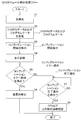
- step S1 peripheral circuits (for example, a bus controller) of the CPU 21 provided in the CPU module 20 are initialized. Then, the process proceeds to step S2.
- peripheral circuits for example, a bus controller
- step S2 the CONFIG data 231a and the program data 232a stored in the FLASH memory 23 are transmitted to the RAM 32 of the signal processing module 30.
- the CONFIG data 231 a and the program data 232 a transmitted from the CPU module 20 to the signal processing module 30 are stored in the RAM 32 of the signal processing module 30. Then, the process proceeds to step S3.
- step S3 a signal (configuration start instruction) for instructing to start configuration is output from the CPU 21 to the FPGA 33 of the signal processing module 30. Then, the process proceeds to step S4.
- step S4 a self-diagnosis by the CPU 21 is performed. Specifically, a validity check of each data stored in the main memory 22 and the FLASH memory 23, a check whether or not the operation of the CPU 21 is normal, and the like are performed.
- the self-diagnosis process in step S4 is performed in parallel with the configuration process of the FPGA 33 of the signal processing module 30 (see steps S12 to S18 in FIG. 4 described later). Then, the process proceeds to step S5.
- the CPU 21 may be configured to perform processing for stopping the entire PLC 100.
- step S5 a configuration error notification output from the signal processing module 30 when any error (configuration error) occurs during the configuration of the FPGA 33 of the signal processing module 30 (step S14 in FIG. 4 described later). And S15) is determined on the CPU module 20 side.
- step S5 if a configuration error notification is detected in step S5, the process proceeds to step S6.
- step S6 a process for stopping the entire PLC 100 is performed, and the process ends.
- step S5 if no configuration error notification is detected in step S5, the process proceeds to step S7.
- step S7 whether or not a configuration completion notification (see steps S16 and S17 in FIG. 4 described later) output from the signal processing module 30 when the configuration of the FPGA 33 of the signal processing module 30 is completed is detected. Is judged.
- step S7 is repeated until a configuration completion notification is detected.
- step S7 when a configuration completion notification is detected, the process proceeds to step S8.
- step S8 a connection confirmation is made as to whether or not the connection with the FPGA 33 (CPU core 33a is normal) after the configuration. Then, the process is terminated. If any abnormality is detected in the connection with the CPU core 33a in step S8, the CPU 21 may be configured to perform processing for stopping the entire PLC 100.
- step S11 the SRAM or the like in the FPGA 33 is initialized.
- the configuration start instruction transmitted from the CPU module 20 in step S2 in FIG. 3 and stored in the RAM 32 and output from the CPU module 20 in step S3 in FIG. 3 is detected on the signal processing module 30 side. If YES, go to step S12.
- step S 12 the CONFIG data 231 a transmitted from the CPU module 20 and stored in the RAM 32 in step S 2 of FIG. 3 is read from the RAM 32. Then, the process proceeds to step S13.
- step S13 the configuration of the FPGA 33 is started based on the CONFIG data 231a read from the RAM 32 in step S12. Then, the process proceeds to step S14.
- step S14 it is determined whether an error (configuration error) has occurred during the configuration of the FPGA 33. If it is determined in step S14 that a configuration error has occurred, the process proceeds to step S15. In step S15, a signal (configuration error notification) for notifying that a configuration error has occurred is output to the CPU module 20, and the process is terminated.
- step S14 determines whether the configuration is completed. If it is determined in step S14 that no configuration error has occurred, the process proceeds to step S16. In step S16, it is determined whether the configuration is completed. The process of step S16 is repeated until it is determined that the configuration is completed.
- step S16 If it is determined in step S16 that the configuration has been completed, the process proceeds to step S17.
- step S17 a signal (configuration completion notification) for notifying that the configuration is completed is output to the CPU module 20, and the process proceeds to step S18.
- step S18 the operation of the FPGA 33 as the CPU core 33a is started based on the program data 232a transmitted from the CPU 21 in step S2 of FIG. 3 and stored in the RAM 32, and the process ends.
- the processing in steps S12 to S18 (FPGA 33 configuration processing) is performed in parallel with the self-diagnosis processing of the CPU module 20 in step S4 in FIG.
- the CONFIG data 231a (the FPGA 33 of the signal processing module 30) acquired from the CPU module 20 of the PLC 100 is included in the signal processing module 30 (image processing module 30a) of the PLC 100.
- a volatile RAM 32 for storing configuration information for programming to function as the CPU core 33a is provided.
- the FPGA 33 that functions as the CPU core 33 a by the configuration is configured to be accessible to the RAM 32.
- the volatile RAM 32 of the signal processing module 30 in which the CONFIG data 231a of the FPGA 33 is stored can be used as a memory for storing various data used when the FPGA 33 after configuration operates as the CPU core 33a. Can be used.
- the signal processing module 30 can be reduced in size.
- the program data 232a of the CPU core 33a is also stored in the RAM 32 of the signal processing module 30 (image processing module 30a), and the CPU core 33a is operated based on the program data 232a stored in the RAM 32. .
- the signal processing module 30 can be further downsized.
- the RAM 32 of the signal processing module 30 (image processing module 30a) is used as a working memory for the CPU core 33a.
- the signal processing module 30 can be further reduced in size.
- the RAM 32 of the signal processing module 30 (image processing module 30a) is configured to be accessible from the CPU 21 of the CPU module 20.
- the convenience of control can be improved.
- the access control unit 34 of the signal processing module 30 (image processing module 30 a) arbitrates contention for the right to use the bus 36 b connected to the RAM 32, thereby transferring to the RAM 32. Control access. Thereby, it is possible to easily avoid the access control unit 34 from competing for access to the RAM 32.
- the FPGA 33 of the signal processing module 30 (image processing module 30a) is configured in parallel with the self-diagnosis of the CPU module 20. Thereby, the configuration of the FPGA 33 of the signal processing module 30 (image processing module 30a) and the self-diagnosis of the CPU module 20 can be efficiently performed.
- a plurality of signal processing modules 30 are provided, and the configuration of the FPGA 33 of each of the plurality of signal processing modules 30 is performed in parallel with the self-diagnosis of the CPU module 20. To do. Thereby, even when there are a plurality of signal processing modules 30, the configuration of the FPGA 33 of each of the plurality of signal processing modules 30 and the self-diagnosis of the CPU module 20 can be performed efficiently.
- the camera 32 connected to the signal processing module 30 (image processing module 30a) is connected to the RAM 32 without the CPU core 33a.
- a DMA controller 35 is provided for enabling access to the network.
- the image data input from the camera 200 connected to the signal processing module 30 is also stored in the RAM 32 of the signal processing module 30 (image processing module 30a).
- the signal processing module 30 can be further downsized.
- a PLC (programmable logic controller) 101 (programmable logic controller) 101 according to the second embodiment will be described with reference to FIG.
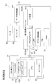
- the motor control device 303 connected to the motor 301 and the encoder 302 is connected to the signal processing module 30.
- the PLC 101 is an example of a “control device”.
- the motor control device 303 is an example of an “external input device”.
- the motor control device 303 connected to the motor 301 and the encoder 302 is connected to the signal processing module 30 of the PLC 101 according to the second embodiment via a cable 43.
- the FPGA 33 of the signal processing module 30 is configured as a CPU core 33b of the signal processing module 30b for performing signal processing on feedback from the encoder 302 or the like by a configuration performed when the PLC 101 is powered on. Programmed to function.
- the I / F circuit 31b of the signal processing module 30 is configured to include a circuit corresponding to an analog signal, a PWM signal, or the like output to the motor control device 303 via the cable 43. ing.
- the CONFIG data 231b including information (configuration information) for programming the FPGA 33 of the signal processing module 30 to function as the CPU core 33b in the FLASH memory 23 of the CPU module 20 of the PLC 101; Further, program data 232b including an operation program for operating the configured FPGA 33 as the CPU core 33b is stored.
- These CONFIG data 231b and program data 232b are transmitted from the CPU module 20 side to the signal processing module 30b side when the PLC 101 is turned on, and stored in the RAM 32 of the signal processing module 30b, as in the first embodiment. .
- the signal processing module 30 is provided with a RAM 32 that is a volatile random access memory and an FPGA 33 that is a field programmable gate array of SRAM.
- the FPGA 33 is configured to be programmed as a CPU core 33b for performing signal processing (motor control) with respect to feedback from the encoder 302 or the like by a configuration performed based on the CONFIG data 231b stored in the RAM 32.
- the FPGA 33 programmed as the CPU core 33b for performing signal processing in this way is configured to operate based on the program data 232b stored in the RAM 32.
- the FPGA 33 (CPU core 33b) after configuration is configured to be accessible to the RAM 32. That is, the RAM 32 is configured to be used as a working memory when the FPGA 33 (CPU core 33b) after configuration performs signal processing on feedback from the encoder 302 and the like.
- processing flow at the time of power-on of the PLC 101 according to the second embodiment is also the first embodiment (FIGS. 3 and 4). See).
- a PLC control device
- a CPU module including a CPU
- a signal processing module including an FPGA (field programmable gate array) and a RAM (volatile memory).
- FPGA field programmable gate array
- RAM volatile memory
- the signal processing module 30 of the PLC 100 functions as the image processing module 30 a to which the camera 200 is connected is shown.
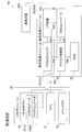
- the signal processing module 30 of the PLC 102 includes an image processing apparatus 400 including a camera 401, an A / D converter (analog / digital converter) 402, a memory 403, and an image processing unit 404. You may make it function as the signal processing module 30c connected.
- the PLC 102 is an example of a “control device”.
- the image processing apparatus 400 is an example of an “external input device”.
- the FPGA 33 of the signal processing module 30 converts the image data after image processing by the A / D converter 402 and the image processing unit 404 in the image processing device 404 according to the configuration. It is programmed to function as the CPU core 33c of the signal processing module 30c that performs predetermined signal processing.
- the I / F circuit 31c of the signal processing module 30 is configured to include a circuit having a serial communication function.
- the configuration according to the first modification shown in FIG. 6 is similar to that of the first embodiment shown in FIGS. 1 to 4 from the FLASH memory 23 of the CPU module 20 to the signal processing module 30 (30c). This is performed based on the CONFIG data 231c transferred to and stored in the volatile RAM 32. Further, the FPGA 33 (CPU core 33c) after configuration according to the first modification shown in FIG. 6 is transferred from the FLASH memory 23 of the CPU module 20 to the RAM 32 of the signal processing module 30 (30c) and stored. It operates based on H.232c.
- the FPGA 33 (CPU core 33c) after configuration is accessible to the RAM 32 as in the first embodiment shown in FIGS. It is configured. That is, the RAM 32 is configured to be used as a working memory when the FPGA 33 (CPU core 33b) after configuration performs predetermined signal processing.
- the image processing apparatus 400 can access the RAM 32 without going through the FPGA 33 (CPU core 33b). It is not necessary to provide the signal processing module 30c with a DMA controller (direct memory access control unit) for this purpose, so that the device configuration can be simplified.
- DMA controller direct memory access control unit
- the signal processing module 30 of the PLC 100 functions as the image processing module 30 a to which the camera 200 is connected is shown.
- the signal processing module 30 of the PLC 103 may function as the communication processing module 30d to which the communication device 500 is connected.
- the PLC 103 is an example of a “control device”.
- the communication device 500 is an example of an “external input device”.
- the FPGA 33 of the signal processing module 30 is configured as a CPU core 33 d of the communication processing module 30 d that performs predetermined signal processing on data input from the communication device 500 by configuration. Programmed to function.
- the I / F circuit 31d of the signal processing module 30 is configured to include a circuit having a serial communication function.
- the configuration according to the second modified example shown in FIG. 7 is similar to the first embodiment shown in FIGS. 1 to 4 in that the volatile memory of the signal processing module 30d from the FLASH memory 23 of the CPU module 20 is used. This is performed based on the CONFIG data 231d transferred to and stored in the RAM 32. Further, the FPGA 33 (CPU core 33d) after configuration according to the second modification shown in FIG. 7 is based on the program data 232d transferred from the FLASH memory 23 of the CPU module 20 to the RAM 32 of the signal processing module 30d and stored. Works.
- the FPGA 33 (CPU core 33d) after configuration is accessible to the RAM 32 as in the first embodiment shown in FIGS. It is configured. That is, the RAM 32 is configured to be used as a working memory when the FPGA 33 (CPU core 33d) after configuration performs signal processing on data input from the communication device 500 or the like.
- the signal processing module 30 (communication processing module 30d) is provided with a DMA controller 35. It has been. As a result, when the amount of data input from the communication device 500 is large and when the data transfer rate is high, the large amount of data is directly transferred to the RAM 32 without the CPU core 33d. Can be transferred to. As a result, data transfer within the signal processing module 30 (communication processing module 30d) can be speeded up, and the burden on the CPU core 33d during data transfer can be reduced.
- the example which makes the signal processing module 30 of PLC100 function as the signal processing module 30b to which the motor control apparatus 303 connected to the motor 301 and the encoder 302 is connected.
- the signal processing module 30 of the PLC 104 may function as the signal processing module 30e directly connected to the encoder 302 as in the third modification of the first embodiment shown in FIG.
- the PLC 104 is an example of a “control device”.
- the encoder 302 is an example of an “external input device”.
- the FPGA 33 of the signal processing module 30 functions as the CPU core 33e of the signal processing module 30e that performs predetermined signal processing on the signal input from the encoder 302 by configuration. To be programmed.
- the I / F circuit 31 d of the signal processing module 30 is configured to include a circuit corresponding to a signal input from the encoder 302.
- the configuration according to the third modification shown in FIG. 8 is similar to the first embodiment shown in FIGS. 1 to 4 in that the volatile memory of the signal processing module 30 (30e) is transferred from the FLASH memory 23 of the CPU module 20. This is performed based on the CONFIG data 231e transferred to and stored in the RAM 32. Further, the FPGA 33 (CPU core 33e) after configuration according to the third modification shown in FIG. 8 is transferred from the FLASH memory 23 of the CPU module 20 to the RAM 32 of the signal processing module 30 (30e) and stored. It operates based on H.232e.
- the FPGA 33 (CPU core 33e) after configuration is accessible to the RAM 32 as in the first embodiment shown in FIGS. It is configured. That is, the RAM 32 is configured to be used as a working memory when the FPGA 33 (CPU core 33e) after configuration performs predetermined signal processing.
- the encoder 302 can access the RAM 32 without going through the FPGA 33 (CPU core 33e). Since it is not necessary to provide the DMA controller (direct memory access control unit) in the signal processing module 30e, the apparatus configuration can be simplified.
- the access control unit 34 is configured by a PLD (program logic device) that is programmed to have a function of arbitrating contention for the right to use the bus 36b connected to the RAM 32.
- PLD program logic device
- the access control unit 34 may be configured by a dedicated device instead of the PLD.
Landscapes
- Engineering & Computer Science (AREA)
- Theoretical Computer Science (AREA)
- Physics & Mathematics (AREA)
- General Engineering & Computer Science (AREA)
- General Physics & Mathematics (AREA)
- Computer Hardware Design (AREA)
- Mathematical Physics (AREA)
- Human Computer Interaction (AREA)
- Quality & Reliability (AREA)
- Computing Systems (AREA)
- Automation & Control Theory (AREA)
- Logic Circuits (AREA)
- Programmable Controllers (AREA)
Priority Applications (3)
| Application Number | Priority Date | Filing Date | Title |
|---|---|---|---|
| CN201280070602.3A CN104137063A (zh) | 2012-02-28 | 2012-02-28 | 控制装置以及控制装置的控制方法 |
| PCT/JP2012/054969 WO2013128578A1 (fr) | 2012-02-28 | 2012-02-28 | Appareil de commande et procédé de commande d'un appareil de commande |
| US14/468,340 US20140365708A1 (en) | 2012-02-28 | 2014-08-26 | Control apparatus and method for controlling control apparatus |
Applications Claiming Priority (1)
| Application Number | Priority Date | Filing Date | Title |
|---|---|---|---|
| PCT/JP2012/054969 WO2013128578A1 (fr) | 2012-02-28 | 2012-02-28 | Appareil de commande et procédé de commande d'un appareil de commande |
Related Child Applications (1)
| Application Number | Title | Priority Date | Filing Date |
|---|---|---|---|
| US14/468,340 Continuation US20140365708A1 (en) | 2012-02-28 | 2014-08-26 | Control apparatus and method for controlling control apparatus |
Publications (1)
| Publication Number | Publication Date |
|---|---|
| WO2013128578A1 true WO2013128578A1 (fr) | 2013-09-06 |
Family
ID=49081830
Family Applications (1)
| Application Number | Title | Priority Date | Filing Date |
|---|---|---|---|
| PCT/JP2012/054969 Ceased WO2013128578A1 (fr) | 2012-02-28 | 2012-02-28 | Appareil de commande et procédé de commande d'un appareil de commande |
Country Status (3)
| Country | Link |
|---|---|
| US (1) | US20140365708A1 (fr) |
| CN (1) | CN104137063A (fr) |
| WO (1) | WO2013128578A1 (fr) |
Cited By (1)
| Publication number | Priority date | Publication date | Assignee | Title |
|---|---|---|---|---|
| CN106133703A (zh) * | 2014-04-03 | 2016-11-16 | 斯特拉托斯卡莱有限公司 | 使用rdma来扫描内存用于删除重复 |
Families Citing this family (7)
| Publication number | Priority date | Publication date | Assignee | Title |
|---|---|---|---|---|
| EP3126984A4 (fr) | 2014-04-03 | 2017-10-11 | Strato Scale Ltd. | Gestion de mémoire au niveau d'un groupe utilisant des signatures de préservation de similarité |
| US9912748B2 (en) | 2015-01-12 | 2018-03-06 | Strato Scale Ltd. | Synchronization of snapshots in a distributed storage system |
| WO2016135570A1 (fr) | 2015-02-26 | 2016-09-01 | Strato Scale Ltd. | Utilisation d'une hiérarchie de fréquences d'accès permettant de sélectionner une destination d'éviction |
| US10402140B2 (en) * | 2016-08-10 | 2019-09-03 | Steven MAZUREK | Memory device with display |
| US10963393B1 (en) | 2017-01-13 | 2021-03-30 | Lightbits Labs Ltd. | Storage system and a method for application aware processing |
| JP7259537B2 (ja) * | 2019-05-16 | 2023-04-18 | オムロン株式会社 | 情報処理装置 |
| CN113569525B (zh) * | 2021-06-24 | 2024-07-23 | 合肥松豪电子科技有限公司 | 一种利用sram在fpga验证平台上的验证模型及方法 |
Citations (5)
| Publication number | Priority date | Publication date | Assignee | Title |
|---|---|---|---|---|
| JP2000353950A (ja) * | 1999-04-21 | 2000-12-19 | Lucent Technol Inc | 可解性問題を再構成可能なハードウエアを用いて解く仮想論理システム |
| JP2001144261A (ja) * | 1999-09-27 | 2001-05-25 | Lucent Technol Inc | フィールド・プログラム可能ゲート・アレイにおけるプログラム可能な相互接続ネットワークのオンライン試験 |
| JP2008293226A (ja) * | 2007-05-24 | 2008-12-04 | Renesas Technology Corp | 半導体装置 |
| JP2009070226A (ja) * | 2007-09-14 | 2009-04-02 | Ricoh Co Ltd | マッチング装置 |
| JP2011008519A (ja) * | 2009-06-25 | 2011-01-13 | Fujitsu Semiconductor Ltd | リコンフィグ演算装置を備えるコンピュータシステムおよびリコンフィグ演算装置 |
Family Cites Families (7)
| Publication number | Priority date | Publication date | Assignee | Title |
|---|---|---|---|---|
| WO2004040428A1 (fr) * | 2002-11-01 | 2004-05-13 | Shinya Kobayashi | Dispositif detachable, circuit de commande, microprogramme de circuit de commande, procede de traitement des informations et modele de conception de circuit de commande, et procede d'ouverture de session |
| CN101131648A (zh) * | 2006-08-25 | 2008-02-27 | 深圳迈瑞生物医疗电子股份有限公司 | Usb接口控制面板在线更新方法 |
| CN101593169A (zh) * | 2008-05-30 | 2009-12-02 | 国际商业机器公司 | 可配置逻辑阵列的配置管理器和配置方法 |
| CN101485576A (zh) * | 2008-12-30 | 2009-07-22 | 深圳市蓝韵实业有限公司 | 一种对设备内fpga芯片统一配置和管理的系统 |
| CN101776914A (zh) * | 2009-12-29 | 2010-07-14 | 天津市亚安科技电子有限公司 | 云台自诊断监控电路 |
| JP2012027544A (ja) * | 2010-07-20 | 2012-02-09 | Toshiba Corp | ライトバックキャッシュを備える情報処理装置、及びその主メモリ診断方法 |
| JP2015022363A (ja) * | 2013-07-16 | 2015-02-02 | キヤノン株式会社 | データ転送制御装置、データ転送制御方法、及びプログラム |
-
2012
- 2012-02-28 WO PCT/JP2012/054969 patent/WO2013128578A1/fr not_active Ceased
- 2012-02-28 CN CN201280070602.3A patent/CN104137063A/zh active Pending
-
2014
- 2014-08-26 US US14/468,340 patent/US20140365708A1/en not_active Abandoned
Patent Citations (5)
| Publication number | Priority date | Publication date | Assignee | Title |
|---|---|---|---|---|
| JP2000353950A (ja) * | 1999-04-21 | 2000-12-19 | Lucent Technol Inc | 可解性問題を再構成可能なハードウエアを用いて解く仮想論理システム |
| JP2001144261A (ja) * | 1999-09-27 | 2001-05-25 | Lucent Technol Inc | フィールド・プログラム可能ゲート・アレイにおけるプログラム可能な相互接続ネットワークのオンライン試験 |
| JP2008293226A (ja) * | 2007-05-24 | 2008-12-04 | Renesas Technology Corp | 半導体装置 |
| JP2009070226A (ja) * | 2007-09-14 | 2009-04-02 | Ricoh Co Ltd | マッチング装置 |
| JP2011008519A (ja) * | 2009-06-25 | 2011-01-13 | Fujitsu Semiconductor Ltd | リコンフィグ演算装置を備えるコンピュータシステムおよびリコンフィグ演算装置 |
Cited By (1)
| Publication number | Priority date | Publication date | Assignee | Title |
|---|---|---|---|---|
| CN106133703A (zh) * | 2014-04-03 | 2016-11-16 | 斯特拉托斯卡莱有限公司 | 使用rdma来扫描内存用于删除重复 |
Also Published As
| Publication number | Publication date |
|---|---|
| US20140365708A1 (en) | 2014-12-11 |
| CN104137063A (zh) | 2014-11-05 |
Similar Documents
| Publication | Publication Date | Title |
|---|---|---|
| US20140365708A1 (en) | Control apparatus and method for controlling control apparatus | |
| US10002103B2 (en) | Low-pin microcontroller device with multiple independent microcontrollers | |
| US10324436B2 (en) | System and method for programmable control instruments, test and measurement hardware configuration | |
| US10002102B2 (en) | Low-pin microcontroller device with multiple independent microcontrollers | |
| JP6005222B2 (ja) | デバッグインターフェースを部分的にイネーブルするための装置 | |
| JP6145987B2 (ja) | プログラマブルコントローラ、プログラマブルコントローラのデータバックアップ方法、プログラマブルコントローラの起動方法 | |
| JP2017517067A5 (fr) | ||
| US8386759B1 (en) | Integrated circuit boot method and apparatus for configuring memory device read mode using programmable circuitry boot code read from the memory device | |
| JP6175788B2 (ja) | マイクロプログラムを更新可能な電子機器 | |
| US8316168B2 (en) | Method and communications system for the configuration of a communications module containing a logic component | |
| US12141590B2 (en) | Method, system, and device for software and hardware component boot configuration and content generation | |
| JPWO2013128578A1 (ja) | 制御装置および制御装置の制御方法 | |
| US9971332B2 (en) | Input/output control device, input/output control method, and non-transitory computer-readable medium for selective activation of logical circuits | |
| JP2017520829A (ja) | マルチプロセッサコアデバイスのためにデバイスピン所有権を割り当てるためのデバイスおよび方法 | |
| KR101470168B1 (ko) | 제어기 내 cpu의 리프로그래밍 방법 | |
| JP6048249B2 (ja) | デバイス更新装置、及びデバイス更新方法 | |
| US20180196908A1 (en) | Hardware-configurable logic unit and microcontroller having such a hardware-configurable logic unit | |
| JP2011248456A (ja) | 電子装置およびマイクロコントローラ | |
| JP6343945B2 (ja) | プログラム可能な論理回路デバイスを備えた電子装置 | |
| JP5774941B2 (ja) | コンフィグレーション装置及びコンフィグレーション方法 | |
| US9645556B2 (en) | Automation device | |
| CN102289381A (zh) | 一种可编程逻辑器件的升级方法及系统 | |
| JP4073321B2 (ja) | データ処理装置 | |
| JP6488683B2 (ja) | Fpga用ic基板 | |
| KR100836807B1 (ko) | 외부개발 단계 프로그램 메모리를 갖는 에이에스아이씨 마이크로 컴퓨터 |
Legal Events
| Date | Code | Title | Description |
|---|---|---|---|
| 121 | Ep: the epo has been informed by wipo that ep was designated in this application |
Ref document number: 12869614 Country of ref document: EP Kind code of ref document: A1 |
|
| ENP | Entry into the national phase |
Ref document number: 2014501882 Country of ref document: JP Kind code of ref document: A |
|
| NENP | Non-entry into the national phase |
Ref country code: DE |
|
| 122 | Ep: pct application non-entry in european phase |
Ref document number: 12869614 Country of ref document: EP Kind code of ref document: A1 |