WO2013128583A1 - Dispositif à semi-conducteurs - Google Patents
Dispositif à semi-conducteurs Download PDFInfo
- Publication number
- WO2013128583A1 WO2013128583A1 PCT/JP2012/054997 JP2012054997W WO2013128583A1 WO 2013128583 A1 WO2013128583 A1 WO 2013128583A1 JP 2012054997 W JP2012054997 W JP 2012054997W WO 2013128583 A1 WO2013128583 A1 WO 2013128583A1
- Authority
- WO
- WIPO (PCT)
- Prior art keywords
- region
- semiconductor device
- semiconductor substrate
- transistor
- protection element
- Prior art date
- Legal status (The legal status is an assumption and is not a legal conclusion. Google has not performed a legal analysis and makes no representation as to the accuracy of the status listed.)
- Ceased
Links
Images













Classifications
-
- H—ELECTRICITY
- H10—SEMICONDUCTOR DEVICES; ELECTRIC SOLID-STATE DEVICES NOT OTHERWISE PROVIDED FOR
- H10D—INORGANIC ELECTRIC SEMICONDUCTOR DEVICES
- H10D89/00—Aspects of integrated devices not covered by groups H10D84/00 - H10D88/00
- H10D89/60—Integrated devices comprising arrangements for electrical or thermal protection, e.g. protection circuits against electrostatic discharge [ESD]
-
- H—ELECTRICITY
- H10—SEMICONDUCTOR DEVICES; ELECTRIC SOLID-STATE DEVICES NOT OTHERWISE PROVIDED FOR
- H10D—INORGANIC ELECTRIC SEMICONDUCTOR DEVICES
- H10D84/00—Integrated devices formed in or on semiconductor substrates that comprise only semiconducting layers, e.g. on Si wafers or on GaAs-on-Si wafers
- H10D84/40—Integrated devices formed in or on semiconductor substrates that comprise only semiconducting layers, e.g. on Si wafers or on GaAs-on-Si wafers characterised by the integration of at least one component covered by groups H10D12/00 or H10D30/00 with at least one component covered by groups H10D10/00 or H10D18/00, e.g. integration of IGFETs with BJTs
- H10D84/401—Combinations of FETs or IGBTs with BJTs
-
- H—ELECTRICITY
- H10—SEMICONDUCTOR DEVICES; ELECTRIC SOLID-STATE DEVICES NOT OTHERWISE PROVIDED FOR
- H10D—INORGANIC ELECTRIC SEMICONDUCTOR DEVICES
- H10D89/00—Aspects of integrated devices not covered by groups H10D84/00 - H10D88/00
- H10D89/60—Integrated devices comprising arrangements for electrical or thermal protection, e.g. protection circuits against electrostatic discharge [ESD]
- H10D89/601—Integrated devices comprising arrangements for electrical or thermal protection, e.g. protection circuits against electrostatic discharge [ESD] for devices having insulated gate electrodes, e.g. for IGFETs or IGBTs
- H10D89/711—Integrated devices comprising arrangements for electrical or thermal protection, e.g. protection circuits against electrostatic discharge [ESD] for devices having insulated gate electrodes, e.g. for IGFETs or IGBTs using bipolar transistors as protective elements
- H10D89/713—Integrated devices comprising arrangements for electrical or thermal protection, e.g. protection circuits against electrostatic discharge [ESD] for devices having insulated gate electrodes, e.g. for IGFETs or IGBTs using bipolar transistors as protective elements including a PNP transistor and a NPN transistor, wherein each of said transistors has its base region coupled to the collector region of the other transistor, e.g. silicon controlled rectifier [SCR] devices
Definitions
- the present invention relates to a semiconductor device in which an element for protecting a bipolar transistor or a junction field effect transistor used in an input circuit of a semiconductor device from electrostatic discharge (ESD) is formed, and in particular, formation of the protective element.
- the present invention relates to a semiconductor device in which an additional process is suppressed and the occupied area is reduced.
- semiconductor devices such as semiconductor integrated circuits are used in many fields including consumer applications such as mobile communication terminals, display devices, and notebook PCs, and industrial applications such as various production facilities and factory robots. ing.
- consumer applications such as mobile communication terminals, display devices, and notebook PCs
- industrial applications such as various production facilities and factory robots.
- the level of reliability required is increased, and particularly high reliability is required particularly in the use field related to human life such as medical equipment and transportation equipment.
- a semiconductor device having a general structure formed on a semiconductor substrate is extremely vulnerable to electrostatic discharge caused by contact with a charged person, etc., coupled with miniaturization of wiring rules on the substrate. Therefore, in order to protect such a semiconductor device from electrostatic discharge, the input circuit of the semiconductor device is provided with an ESD protection element.
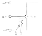
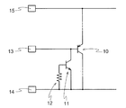
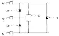
- FIG. 28 and 29 are circuit diagrams showing the periphery of the protective element of the input circuit of the semiconductor device according to the prior art.
- a diode 30 is connected as an ESD protection element between the input terminal 13 and the high voltage source terminal 15 or the low voltage source terminal 14, and each element of the input circuit is utilized by using the breakdown of the PN junction. We are trying to protect.
- the ESD protection element 31 is connected between the input terminal 13 and the low voltage source terminal 14.
- the ESD protection element 31 includes several circuit elements, and is disclosed in, for example, Patent Document 1, Patent Document 2, and Patent Document 3.
- the ESD protection element described in Patent Document 1 and Patent Document 2 uses the breakdown of the PN junction of the transistor inside thereof, and the ESD protection element described in Patent Document 3 is an overvoltage application by ESD. Accordingly, the Zener diode and the field effect transistor inside thereof are operated to function as a protective element.
- a dedicated protection element is formed between the terminal of each voltage source and the input terminal for ESD protection of the bipolar transistor and the junction field effect transistor used in the input circuit. For this reason, in addition to the region necessary for the original function of the semiconductor device, a region corresponding to the size and quantity of the protection element itself is required, which increases the area of the entire semiconductor device. .
- the protection element in order for the protection element to protect the transistor of the input circuit, the protection element needs to function at a voltage lower than the element breakdown voltage of the transistor of the input circuit. It is necessary to form by a different process. There is also a problem that the manufacturing cost of the semiconductor device is increased due to this additional process.
- the protection element according to the prior art is additionally connected to the base terminal of the transistor of the input circuit, there is a risk of affecting the characteristics of the input circuit, and the parasitic capacitance, leakage current, and noise of the input circuit are reduced. There is also a problem that the performance of the semiconductor device may be lowered as a result.
- the present invention has been made to solve such a problem, and can be formed with a small area and no additional process in comparison with the protection element according to the prior art, and the performance of the semiconductor device can be improved. It is an object of the present invention to provide a semiconductor device including a protection element that can protect an ESD of a transistor of an input circuit without causing a decrease.
- a trigger mechanism that determines the voltage at which the protection element operates, and a mechanism that passes a current to suppress the ESD voltage.
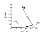
- the inventors of the present invention use a PN formed between an N-type region as a base and a P-type semiconductor substrate as a collector in a PNP transistor formed in a semiconductor device. It has been found that the junction does not immediately break by application of a voltage exceeding the breakdown voltage due to ESD. That is, FIG.
- FIG. 27 shows the current-voltage at the time of breakdown of the PN junction obtained by using a device called TLP (Transmission Line Pulser) for evaluating the current-voltage characteristics of the circuit element against the application of surge voltage.
- TLP Transmission Line Pulser
- the inventors of the present invention have further studied diligently, and an NPN transistor in which a junction between the base and collector (P-type semiconductor substrate) of this PNP transistor is formed as a collector-base junction as an element operating within the voltage range described above.
- the collector-base of this NPN transistor is broken down, the NPN transistor is turned on by the current that flows thereafter, and the ESD current is passed through this transistor to form a P-type semiconductor.
- a method of flowing on a substrate was found.
- This NPN transistor can be formed with the base region of the PNP transistor as a collector and the P-type semiconductor substrate as a base only by providing an N-type region serving as an emitter on the P-type semiconductor substrate.
- the NPN transistor itself is turned on by the potential difference between the base and emitter of the transistor, and a current caused by ESD can flow through the P-type semiconductor substrate through the transistor.
- a semiconductor device includes a first conductivity type semiconductor substrate and a first region of a second conductivity type semiconductor layer formed on a surface of the semiconductor substrate, and is formed by the semiconductor substrate and the first region.
- a semiconductor device comprising: a circuit element including a PN junction; an input terminal connected to the first region; and a protection element protecting the circuit element from ESD applied to the input terminal.
- the transistor is formed using the first region as a collector, the semiconductor substrate as a base, and the second region as an emitter.
- the emitter and the semiconductor substrate are formed by being connected by a conductor through a connection region provided in the semiconductor substrate.
- connection region provided in the semiconductor substrate is provided between the first region and the second region, the voltage generated between the base and the emitter of the transistor is reduced, and the transistor is turned on. Since there is a possibility of disappearing, it is preferable that the connection region is disposed on the side opposite to the side facing the first region.
- the first region is formed separately, a plurality of circuit elements using each of the plurality of first regions are formed, and the second region of the protection element is the plurality of the plurality of circuit elements.
- One piece may be formed in an intermediate portion sandwiched between the first regions.
- At least part of the outer peripheral shape of the first region in the semiconductor substrate surface is curved, and the outer peripheral shape of the portion of the second region that is formed adjacent to the first region and that faces the first region is A curve along the curve of the first region is preferable in that the protection element 11 maintains the capability of flowing current due to ESD while increasing the breakdown voltage of the PN junction.
- the second conductivity type region having a higher impurity concentration than that of the first region may be formed in the lower layer of the first region, and the lower layer of the second region may be formed in a structure in direct contact with the semiconductor substrate.
- the second conductive type semiconductor layer is formed by epitaxial growth on the semiconductor substrate, and the first and second regions are formed by implanting a first conductive type impurity into the epitaxial layer and separating the epitaxial layer. May be.
- the circuit element may be a vertical bipolar transistor having the first region as a base, collector or emitter, or a lateral bipolar transistor having the first region as a base, collector or emitter, or the first region as a gate.
- a junction field effect transistor may be used as a source or a drain.
- the protection element that protects the circuit element of the input stage that constitutes the integrated circuit includes the first conductivity type semiconductor substrate that constitutes the circuit element, and the second conductivity type first that is formed on the surface thereof. Since each of the regions is a base and a collector, and a second conductivity type second region formed on the semiconductor substrate is a transistor, and the emitter and the semiconductor substrate are connected by a conductor, the first Even when ESD is applied to one region and a breakdown current flows through the PN junction between the first region and the semiconductor substrate, a voltage generated by the breakdown current flowing in the semiconductor substrate and the intrinsic resistance of the semiconductor substrate is formed as a protective element. Applied between the base and emitter of the transistor to turn on the transistor.
- the transistor since the first region of the second conductivity type semiconductor layer of the circuit element constituting the input stage of the integrated circuit and the semiconductor substrate are respectively used as the collector and base of the protection element, the transistor is constituted.
- the emitter As the second region of the second conductivity type semiconductor layer on the surface of the semiconductor substrate, a transistor of the protection element can be formed, and a potential difference between the base and the emitter for turning on the transistor is generated.
- the resistance element uses the specific resistance of the semiconductor substrate, the space for forming the protection element is to connect the second region of the second conductivity type semiconductor layer as the emitter and the emitter to the semiconductor substrate.
- the protective element can be formed in a space only for the connection region formed on the surface of the semiconductor substrate. As a result, the protective element can be formed with a much smaller occupied area than the space for forming a conventional diode or transistor and its associated elements.
- the transistor of the protection element is formed using the region of the circuit element.
- the PN junction for forming the element is the same for the circuit element and the protection element. Since the breakdown voltage is lower than that of the element to be protected, unlike the conventional protection element, it is not necessary to yield before the element to be protected. Therefore, the protection element is formed by a special process. There is no need, and the protective element can be formed only by a process of forming a normal circuit element. Therefore, the number of steps for forming the protective element can be greatly reduced, and the protection element can be formed at a very low cost.
- the present invention since there is no need to connect an additional protective element to the terminal of a circuit element such as an integrated circuit to be protected, there is no possibility of affecting the performance of the original circuit element.
- the circuit elements of the integrated circuit can be protected without degrading the performance.
- FIG. 3 is a cross-sectional explanatory diagram in which an equivalent circuit is written in a schematic cross section of the periphery of the protective element of the semiconductor device according to the first embodiment of the present invention.
- FIG. 3 is an equivalent circuit diagram of the periphery of the protection element of the semiconductor device according to the first embodiment of the present invention.
- FIG. 5 is measurement data of current-voltage characteristics at the time of breakdown between the base and the collector of the PNP transistor of the input circuit of the semiconductor device according to the first embodiment of the present invention.
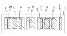
- FIG. 5 is an equivalent circuit diagram of a periphery of a protection element of a semiconductor device according to a second embodiment of the present invention. It is a plane explanatory view showing a protection element peripheral part of a semiconductor device by a 3rd embodiment of the present invention. It is sectional explanatory drawing which wrote the equivalent circuit in the schematic cross section of the protection element periphery part of the semiconductor device by the 3rd Embodiment of this invention.
- FIG. 1 It is an equivalent circuit schematic of the protection element periphery part of the semiconductor device by the 3rd Embodiment of this invention. It is a plane explanatory view showing a protection element peripheral part of a semiconductor device by a 4th embodiment of the present invention. It is sectional explanatory drawing which wrote the equivalent circuit in the schematic cross section of the protection element periphery part of the semiconductor device by the 4th Embodiment of this invention. It is an equivalent circuit schematic of the protection element periphery part of the semiconductor device by the 4th Embodiment of this invention. It is a plane explanatory view showing a protection element peripheral part of a semiconductor device by a 5th embodiment of the present invention. FIG.
- FIG. 10 is a cross-sectional explanatory diagram in which an equivalent circuit is written in a schematic cross section of a periphery of a protective element of a semiconductor device according to a fifth embodiment of the present invention. It is an equivalent circuit schematic of the protection element periphery part of the semiconductor device by the 5th Embodiment of this invention. It is a plane explanatory view showing a protection element peripheral part of a semiconductor device by a 6th embodiment applied to a 1st embodiment of the present invention. It is a plane explanatory view showing a protection element peripheral part of a semiconductor device by a 6th embodiment applied to a 2nd embodiment of the present invention.
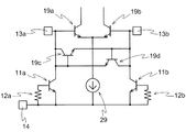
- FIG. 24 is an explanatory cross-sectional view in which the equivalent circuit of FIG. 23 is entered in the schematic cross section of the periphery of the protective element of the semiconductor device according to the eighth embodiment of the present invention. It is an equivalent circuit diagram of the protection element peripheral part of the semiconductor device by the 9th Embodiment of this invention.
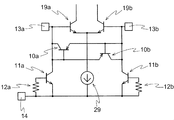
- FIG. 26 is an explanatory cross-sectional view in which the equivalent circuit of FIG. 25 is entered in the schematic cross section of the periphery of the protective element of the semiconductor device according to the ninth embodiment of the present invention.
- This is measurement data of current-voltage characteristics at the time of breakdown between the base and collector of a PNP transistor to which no protective element is connected.
- It is a circuit diagram which shows the protection element periphery part of the input circuit of the semiconductor device by a prior art. It is a circuit diagram which shows the protection element periphery part of the other input circuit of the semiconductor device by a prior art.
- the semiconductor device according to the present invention has a first conductivity type semiconductor substrate (shown in FIGS. 1 to 3), as shown in FIGS. In the example, it has a first region 2 of a P-type semiconductor substrate) 1 and a second conductivity type semiconductor layer (N-type epitaxial semiconductor layer in the example shown in FIGS. 1 to 3) formed on the surface of the semiconductor substrate 1.
- the protective element (NPN transistor) 11 is formed by forming the second region 6 of the second conductivity type semiconductor layer on the semiconductor substrate 1, thereby using the first region 2 as a collector and the semiconductor substrate 1 as a base. And an NPN transistor 11 formed with the second region 6 as an emitter, and the emitter (second region 6) and the semiconductor substrate 1 are connected to each other by a conductor 7 via a connection portion 8 provided in the semiconductor substrate 1. Is formed.
- the circuit element 10 has a P-type region formed in the first region 2 as an emitter 3, a first region 2 as a base, and a P-type semiconductor substrate 1 as a collector.
- the PNP transistor 10 is an example of a semiconductor integrated circuit that forms an input stage. An input terminal is connected to the base (first region 2) of the PNP transistor 10 via a contact region 5. 13 is formed.
- the configuration of the input stage is not limited to this example, and as will be described later, the ESD protection element of the present invention can be used in various cases such as a lateral PNP transistor or a P-channel junction field effect transistor.
- reference numeral 4 denotes a collector of the PNP transistor 10, a contact region made of a P-type semiconductor provided on the semiconductor substrate 1, and 9 denotes a decrease in breakdown voltage between the collector and the emitter formed in the lower layer of the first region 2.
- 14 is a low voltage source terminal of the semiconductor substrate 1 corresponding to the collector of the PNP transistor 10, and 15 is a high voltage source terminal.
- the protection element 11 is formed by forming the second region 6 of the second conductivity type (N-type) semiconductor layer formed on the surface side of the semiconductor substrate 1.
- An NPN transistor 11 having a collector 2, a semiconductor substrate 1 as a base, and a second region 6 as an emitter is formed.
- the second region 6 serving as the emitter is connected to a connection region (contact region) 8 provided on the surface of the semiconductor substrate 1 through a contact region 6a by a conductor 7 made of, for example, aluminum.
- the base and emitter of the NPN transistor 11 are connected via the parasitic resistance 12 of the semiconductor substrate 1.
- connection region 8 of the semiconductor substrate 1 is formed on the opposite side of the second region 6 from the first region 2. Although it is possible to arrange the connection region 8 at another location of the semiconductor substrate 1, it is preferable to arrange the connection region 8 at a position as in the present embodiment. The reason is that when an ESD voltage is applied as described later, the base-collector PN junction of the NPN transistor 11 breaks down, and a current flows through the parasitic resistance 12 of the P-type semiconductor substrate 1. -A potential difference is generated between the emitters and the NPN transistor 11 is turned on. However, if the connection region 8 is provided between the first region 2 and the second region 6, the path through which this current flows in the semiconductor substrate 1 is shortened. This is because when the substantial resistance value of the parasitic resistance 12 is lowered, the potential difference generated between the base and the emitter of the NPN transistor 11 does not reach a predetermined value, and this transistor may not be turned on.
- the buried layer 9 having a higher impurity concentration than the first region 2 is formed in the lower layer of the first region 2, but such a buried region is formed in the lower layer of the second region 6. Is not formed and is in direct contact with the semiconductor substrate 1.
- the area necessary for forming the protection element 11 is the above-described second region 6 and the semiconductor substrate. It is only necessary to increase the area of only the connection region 8 formed in 1.
- an area of, for example, 7298 ⁇ m 2 was required, but according to the present embodiment, it was confirmed that it can be formed with, for example, 1504 ⁇ m 2.
- the effect of reducing the area increased for forming the protective element by about 80% is obtained with respect to the protective element by the technology.
- FIG. 2 This structure is shown in an equivalent circuit diagram as shown in FIG. 2 also shows the PNP transistor 10, the NPN transistor 11 as a protection element, and the parasitic resistance 12 between the base and the emitter. As apparent from FIG. 3, the NPN transistor 11 as a protection element is connected between the input terminal 13 and the low voltage source terminal 14.
- the PN junction is not immediately destroyed, so the current flowing through the semiconductor substrate during that time causes the base of the NPN transistor 11 to If the specific resistance (impurity concentration) of the semiconductor substrate is set so that the voltage between the emitters reaches the threshold voltage at which the NPN transistor 11 is turned on and the NPN transistor 11 is turned on, after breakdown The NPN transistor 11 is turned on before the breakdown, and the current after breakdown can be released to the semiconductor substrate side through the NPN transistor 11, so that the breakdown of the PN junction can be prevented.
- the specific resistance (impurity concentration) of the semiconductor substrate is set so that the voltage between the emitters reaches the threshold voltage at which the NPN transistor 11 is turned on and the NPN transistor 11 is turned on, after breakdown
- the NPN transistor 11 is turned on before the breakdown, and the current after breakdown can be released to the semiconductor substrate side through the NPN transistor 11, so that the breakdown of the PN junction can be prevented.
- the PNP transistor 10 can be protected by turning on the NPN transistor 11 serving as a protection element.
- FIG. 4 shows measurement data of current-voltage characteristics at the time of breakdown between the base and the collector of the PNP transistor 10 of the input circuit of the semiconductor device according to the present embodiment, which was measured by the same method as the measurement data shown in FIG. It is.
- the specific resistance of the P-type semiconductor substrate is set to about 5 to 50 ⁇ ⁇ cm, and the first and second described above are used.
- the depth of the region from the surface of the semiconductor device is in the range of about 3 to 20 ⁇ m, the voltage at which the NPN transistor 11 as the protection element is turned on is significantly increased, the current gain of the transistor is significantly decreased, or A value that does not cause punch-through is preferable.
- the semiconductor device according to the present invention does not require any additional process, it can be manufactured by a general semiconductor device process.
- the first region 2 and the second region 6 made of the N-type semiconductor are formed on the semiconductor substrate by epitaxial growth, and then doped with the same P-type impurity as the conductivity type of the semiconductor substrate. May be formed by isolating, or may be formed by annealing after injecting an N-type impurity into a P-type semiconductor substrate.
- the semiconductor substrate 1 is described as an example of P type, the first region as an N type, the circuit element as a PNP transistor, and the protection element as an NPN transistor.
- the function as the protective element can be exhibited similarly.
- the transistor of the protection element functions against a negative overvoltage applied to the input terminal 13 with respect to the semiconductor substrate. The same applies to the following embodiments.
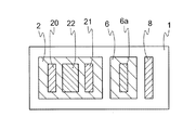
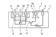
- FIGS. 5 to 7 are a plan view, a cross-sectional view, and an equivalent circuit diagram of the semiconductor structure of the semiconductor device according to the second embodiment of the present invention.
- This embodiment is different from the first embodiment in that the circuit element is a lateral PNP transistor.
- the structural difference from the first embodiment is that the collector 4 of the PNP transistor 10 is not the P-type semiconductor substrate 1 in the first embodiment, but the N-type semiconductor described above. This is only a point that is a P-type semiconductor region formed around the emitter 3 of this transistor in the formed first region 2.
- FIG. 7 also differs only in that the collector 4 of the PNP transistor 10 and the base (semiconductor substrate 1) of the protection element 11 are not directly connected.
- the other structure is the same as that of the first embodiment.
- FIGS. 1 and 5 FIGS. 2 and 6, and FIGS. Detailed description is omitted.
- the P-type semiconductor substrate 1 is insulated from the emitter and collector of the PNP transistor 10, the design of the packaging structure and the wiring board on which the semiconductor device is mounted are designed. There is an advantage that the degree of freedom in pattern design is increased.
- the semiconductor device differs from the first embodiment in that the circuit element to be protected is the lateral PNP transistor 10, but if ESD is applied to the input terminal 13, it is the same as in the first embodiment.
- a voltage is applied to the PN junction with the P-type semiconductor substrate 1 through the first region 2 and the buried layer 9 having the high impurity concentration.
- the protection element made up of the NPN transistor 11 is formed, as in the first embodiment, the voltage can be suppressed, and the lateral PNP transistor as a circuit element can be suppressed. 10 is protected.
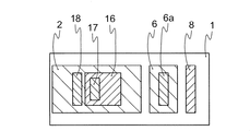
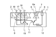
- (Third embodiment) 8 to 10 are a plan view, a cross-sectional view, and an equivalent circuit diagram of the semiconductor structure of the semiconductor device according to the third embodiment of the present invention.
- This embodiment is different from the second embodiment in that the circuit element is an NPN transistor 19 and the input terminal 13 is connected to the collector.
- the NPN transistor 19 has a P-type region formed in the first region 2 with the first region 2 connected to the input terminal 13 through the contact region 18 as a collector.
- the N-type region 17 formed in the P-type region 16 is used as an emitter.
- the equivalent circuit is different in that the input terminal 13 and the collector of the protection element 11 are connected to the collector of the NPN transistor 19 which is a circuit element.
- FIGS. 5 and 8, FIGS. 6 and 9, and FIGS. 7 and 10 correspond to each other. Detailed description thereof will be omitted.
- ESD is applied to the input terminal 13
- a voltage is applied to the PN junction with the P-type semiconductor substrate 1 through the first region 2 and the buried layer 9 as in the first embodiment.
- the protective element 11 is formed as in the first embodiment, the voltage can be suppressed, and the NPN transistor 19 that is a circuit element is protected.
- the NPN transistor 19 is shown as a vertical NPN transistor.
- the NPN transistor 19 is a contact region in the P-type region 16 which is a base and the first region 2 which is a collector.
- the protection element 11 similarly exhibits a function of protecting the circuit element against the application of an ESD voltage to the input terminal 13.
- the first region 2 described above functions as an emitter instead of a collector, and an N-type region 17 formed in the P-type region 16 is not an emitter.
- the protection element 11 is similarly applied to the ESD voltage applied to the input terminal 13. The function to protect the element is demonstrated.
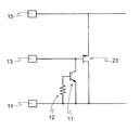
- FIGS. 11 to 13 are a plan view, a cross-sectional view and an equivalent circuit diagram of the semiconductor structure of the semiconductor device according to the fourth embodiment of the present invention.
- the present embodiment is different from the second embodiment in that the circuit element is a P-channel junction field effect transistor 23 and the input terminal 13 is connected to the gate.
- the P-channel junction field effect transistor 23 is formed in the first region 2 with the first region 2 connected to the input terminal 13 through the contact region 22 as a gate.
- the formed P-type region 20 is used as a source, and similarly, the P-type region 21 formed in the first region 2 is used as a drain.
- FIGS. 11 to 13 are a plan view, a cross-sectional view and an equivalent circuit diagram of the semiconductor structure of the semiconductor device according to the fourth embodiment of the present invention.
- the present embodiment is different from the second embodiment in that the circuit element is a P-channel junction field effect transistor 23 and the input terminal 13 is connected to the gate.
- the P-channel junction field effect transistor 23 is formed in the
- the circuit element is a P-channel junction field effect transistor 23, and the collector of the input terminal 13 and the protection element 11 is the P-channel junction field effect transistor 23.
- This is different from the second embodiment in that it is connected to the gate.
- the other structure is the same as that of the second embodiment, and FIGS. 5 and 11, FIGS. 6 and 12, and FIGS. 7 and 13 correspond to each other. Detailed description thereof will be omitted. If ESD is applied to the input terminal 13, a voltage is applied to the PN junction with the P-type semiconductor substrate 1 through the first region 2 and the buried layer 9 as in the first embodiment. However, since the protective element 11 is formed as in the first embodiment, the voltage can be suppressed, and the P-channel junction field effect transistor 23 which is a circuit element is protected.
- FIGS. 14 to 16 are a plan view, a cross-sectional view, and an equivalent circuit diagram of the semiconductor structure of the semiconductor device according to the fifth embodiment of the present invention.
- This embodiment is different from the second embodiment in that the circuit element is an N-channel junction field effect transistor 28 and the input terminal 13 is connected to the drain.
- the N-channel junction field effect transistor 28 has a first region 2 connected to the input terminal 13 through the contact region 26 as a drain, a contact region 27 and a second region.
- a P-type region 24 formed in one region 2 is used as a gate, and an N-type region 25 formed in the P-type region 24 is used as a source.
- the circuit element is an N-channel junction field effect transistor 28, and the input terminal 13 and the collector of the protection element 11 are connected to the N-channel junction field effect transistor 28. It is different from the second embodiment in that it is connected to the drain.
- the other structure is the same as that of the second embodiment, and FIGS. 5 and 14, FIGS. 6 and 15, and FIGS. 7 and 16 correspond to each other. Detailed description thereof will be omitted. If ESD is applied to the input terminal 13, a voltage is applied to the PN junction with the P-type semiconductor substrate 1 through the first region 2 and the buried layer 9 as in the first embodiment. However, since the protective element 11 is formed as in the first embodiment, the voltage can be suppressed, and the N-channel junction field effect transistor 28 that is a circuit element is protected.
- the first region 2 described above functions as a source instead of a drain, and an N-type region 25 formed in the P-type region 24 is not a source but a drain.
- the protection element 11 can prevent the ESD voltage from being applied to the input terminal 13. Similarly, the function of protecting the circuit element is exhibited.
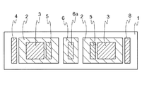
- FIGS. 17 to 19 As illustrated in FIGS. 17 to 19 as plan explanatory views, a circuit is provided in which two first regions 2 of the first, second, and fourth embodiments are provided and protected. In this example, two elements are formed, and the second region 6 constituting the protection element is provided in common therebetween. That is, in FIGS. 17 to 19, each of the base, emitter and collector constituting the first region 2 and the PNP transistor 10 formed therein, and the gate, source and drain constituting the P-channel junction field effect transistor 23 are shown. The regions are formed in line symmetry, and the second region 6, the connection region 8 between the second region 6 and the semiconductor substrate 1, and the collector 4 of the vertical PNP transistor 10 in FIG. However, the respective regions constituting the respective transistors formed in the first region 2 are not necessarily provided in line symmetry, and the collector 4 or the connection region 8 of the vertical PNP transistor 10 is provided in the two first regions. It is also possible to provide one for each region.
- the above-described protection element 11 formed using the first region 2 as a collector is a multi-collector type NPN transistor having two first regions 2 as collectors, and the base is a P-type semiconductor substrate 1 and an emitter. Is formed as the one second region 6 described above. Therefore, since this single protection element 11 can function as a protection element regardless of which of the two first regions 2 is applied with the ESD voltage, one protection element protects two transistors from ESD. can do. Also in this respect, the semiconductor device of the present invention can be formed with a smaller area as compared with a conventional semiconductor device that requires a protection element for each transistor.
- FIG. 17, FIG. 18, and FIG. 19 are diagrams in which this embodiment is applied to the first, second, and fourth embodiments. However, the present embodiment is applied to the third and fifth embodiments. Is also possible.
- FIG. 20 shows an application example of the above-described sixth embodiment.
- the above-mentioned first regions 2 are arranged side by side in the vertical and horizontal directions, and the above-mentioned second regions 6 are arranged between these first regions 2, respectively.
- the protection element 11 described above is formed with the second region 6 as an emitter and all of the first regions 2 arranged adjacent to the periphery thereof as collectors. . Therefore, one protection element 11 can function as a protection element for each transistor formed in four adjacent first regions 2.
- the semiconductor device of the present invention has a larger area reduction effect with respect to the conventional semiconductor device as the number of transistors to be protected increases.
- FIGS. 21 and 22 Each of the embodiments shown in FIGS. 21 and 22 is an example in which the planar shape of the first region 2 of the first and second embodiments is circular.
- the first region 2 has a rectangular shape as shown in FIGS. 17 and 18, when a voltage is applied between the region and the semiconductor substrate 1 on which the region is formed, the rectangular region The electric field concentrates near the apexes of the four corners, and breakdown tends to occur around the corners. Therefore, making the shape of the first region 2 circular has an advantage that the breakdown voltage of the junction between the first region 2 and the P-type semiconductor 1 can be increased.
- the magnitude of the current that can be passed from the collector to the emitter of the protective element 11 of the semiconductor device of the present invention is that the semiconductor substrate 1 having a lower impurity concentration and higher electrical resistance than that of the collector or emitter. It has a relationship inversely proportional to the width of the base of the protection element 11 as the region.
- the substantial width of the base region of the protection element 11 is an interval between the first region that is a collector region and the second region that is disposed adjacent to the first region and serves as an emitter region.
- the shape of the portion facing the first region of the second region disposed adjacent to the first region is the first shape in the outer shape of the first region.
- the shape along the shape of the portion facing the two regions is preferable in terms of maintaining the ability of the protection element 11 to flow a breakdown current due to ESD.
- a part of the shape of the second region is a curved shape shown in FIGS. 21 and 22 based on this idea. There is an advantage that the breakdown voltage can be improved without reducing the flow capability.
- 21 and 22 are examples applied to the structures of the first and second embodiments, but the present invention can also be applied to the structures of the third to fifth embodiments.
- FIGS. 23 and 24 An equivalent circuit diagram and a cross-sectional explanatory diagram of a semiconductor structure of a semiconductor device according to an eighth embodiment of the present invention are shown in FIGS. 23 and 24, respectively.
- This embodiment assumes application to a semiconductor device having a differential input type input circuit including two input terminals, that is, an input terminal 13a and an input terminal 13b.
- the equivalent circuit of this embodiment limits an excessive voltage difference between the input terminals 13a and 13b, a pair of NPN transistors 19a and 19b constituting the differential input unit, and the input terminals 13a and 13b.
- the other NPN transistors 19c and 19d, the protection elements 11a and 11b, the parasitic resistors 12a and 12b of the P-type semiconductor substrate 1, and the current source 29 are included.
- the bases of the NPN transistors 19a and 19b are connected to the input terminals 13a and 13b, the bases and collectors of the NPN transistors 19c and 19d, and the collectors of the protection elements 11a and 11b, respectively. It is connected to the.
- the emitters of the NPN transistors 19c and 19d are connected to the bases of the NPN transistors 19d and 19c. Further, the protection elements 11a and 11b have bases connected to one ends of the parasitic resistors 12a and 12b, respectively, and emitters connected to the low voltage source terminal 14 together with the other ends of the parasitic resistors 12a and 12b and the other end of the current source 29. It is connected.
- the protection elements 11a and 11b are similar to those of the third embodiment. It operates as a protection element for the NPN transistors 19c and 19d.
- the bases of the NPN transistors 19a and 19b are connected to the input terminals 13a and 13b.
- the protection elements 11a and 11b are connected to the input terminals 13a and 13b by applying an NPN to the ESD voltage.
- the transistors 19c and 19d operate as protective elements so as not to be destroyed and the voltage to the collector is suppressed, an excessive voltage that causes destruction is not applied to the bases of the NPN transistors 19a and 19b connected to the collectors.
- substantially the protection elements 11a and 11b can function as all the protection elements of the NPN transistors 19a to 19d.
- FIGS. 25 and 26 An equivalent circuit diagram and a cross-sectional explanatory diagram of the semiconductor structure of the semiconductor device according to the ninth embodiment of the present invention are shown in FIGS. 25 and 26, respectively.
- the set of transistors that limit an excessive voltage difference between the input terminals 13a and 13b is not the NPN transistors 19c and 19d but the PNP transistors 10a and 10b. Is different.
- Other configurations are the same as those of the eighth embodiment including the connection state between the elements, and the same portions are denoted by the same reference numerals, and detailed description thereof is omitted.
- the protection elements 11a and 11b are similar to those of the second embodiment. It operates as a protection element for the PNP transistors 10a and 10b.
- the NPN transistors 19a and 19b are configured such that the bases are connected to the input terminals 13a and 13b, as in the above-described eighth embodiment.
- the protection elements 11a and 11b NPN transistors 19a and 19b connected to the bases operate to protect the PNP transistors 10a and 10b from being destroyed against the application of ESD voltages to the input terminals 13a and 13b and suppress the voltage to the bases. As a result, an excessive voltage that would cause breakdown is not applied to the base of the transistor, and the protection elements 11a and 11b can function as protection elements for all of the PNP transistors 10a and 10b and the NPN transistors 19a and 19b. .
- the semiconductor device according to the present invention can be used in various industrial fields including consumer applications such as display devices and mobile communication terminals, and general industrial applications such as various production facilities. It can be used for portable devices that are easily applied, medical equipment that requires high reliability, and industries related to transportation equipment.
Landscapes
- Semiconductor Integrated Circuits (AREA)
- Bipolar Integrated Circuits (AREA)
- Bipolar Transistors (AREA)
- Metal-Oxide And Bipolar Metal-Oxide Semiconductor Integrated Circuits (AREA)
Abstract
Priority Applications (6)
| Application Number | Priority Date | Filing Date | Title |
|---|---|---|---|
| JP2014501887A JP5764254B2 (ja) | 2012-02-28 | 2012-02-28 | 半導体装置 |
| PCT/JP2012/054997 WO2013128583A1 (fr) | 2012-02-28 | 2012-02-28 | Dispositif à semi-conducteurs |
| KR1020147021445A KR101848352B1 (ko) | 2012-02-28 | 2012-02-28 | 반도체 장치 |
| CN201280070852.7A CN104137251B (zh) | 2012-02-28 | 2012-02-28 | 半导体装置 |
| US14/378,665 US9165919B2 (en) | 2012-02-28 | 2012-02-28 | Semiconductor device |
| TW101143867A TWI545719B (zh) | 2012-02-28 | 2012-11-23 | 半導體裝置 |
Applications Claiming Priority (1)
| Application Number | Priority Date | Filing Date | Title |
|---|---|---|---|
| PCT/JP2012/054997 WO2013128583A1 (fr) | 2012-02-28 | 2012-02-28 | Dispositif à semi-conducteurs |
Publications (1)
| Publication Number | Publication Date |
|---|---|
| WO2013128583A1 true WO2013128583A1 (fr) | 2013-09-06 |
Family
ID=49081833
Family Applications (1)
| Application Number | Title | Priority Date | Filing Date |
|---|---|---|---|
| PCT/JP2012/054997 Ceased WO2013128583A1 (fr) | 2012-02-28 | 2012-02-28 | Dispositif à semi-conducteurs |
Country Status (6)
| Country | Link |
|---|---|
| US (1) | US9165919B2 (fr) |
| JP (1) | JP5764254B2 (fr) |
| KR (1) | KR101848352B1 (fr) |
| CN (1) | CN104137251B (fr) |
| TW (1) | TWI545719B (fr) |
| WO (1) | WO2013128583A1 (fr) |
Families Citing this family (5)
| Publication number | Priority date | Publication date | Assignee | Title |
|---|---|---|---|---|
| US11302687B2 (en) * | 2019-10-30 | 2022-04-12 | Globalfoundries Singapore Pte. Ltd. | Semiconductor device and method of forming the same |
| US11527528B2 (en) * | 2020-04-21 | 2022-12-13 | Globalfoundries Singapore Pte. Ltd. | Electrostatic discharge protection devices and methods of forming electrostatic discharge protection devices |
| CN114188317A (zh) * | 2020-09-15 | 2022-03-15 | 恩智浦有限公司 | 具有保护区和二极管电路的集成电路 |
| CN112397507B (zh) * | 2020-11-16 | 2022-05-10 | 杰华特微电子股份有限公司 | 横向双扩散晶体管及其制造方法 |
| US11611211B2 (en) | 2021-04-19 | 2023-03-21 | Analog Devices, Inc. | Multiple trigger electrostatic discharge (ESD) protection device for integrated circuits with multiple power supply domains |
Citations (4)
| Publication number | Priority date | Publication date | Assignee | Title |
|---|---|---|---|---|
| JPS6123353A (ja) * | 1984-07-11 | 1986-01-31 | Hitachi Ltd | 過電圧保護素子 |
| JP2001267496A (ja) * | 2000-03-17 | 2001-09-28 | Ricoh Co Ltd | 入力保護回路を備えた半導体装置 |
| JP2007173524A (ja) * | 2005-12-22 | 2007-07-05 | Sharp Corp | レギュレータ回路及びそれを用いた半導体装置 |
| JP2008205148A (ja) * | 2007-02-20 | 2008-09-04 | New Japan Radio Co Ltd | 縦型pnpバイポーラトランジスタ用静電破壊保護素子 |
Family Cites Families (8)
| Publication number | Priority date | Publication date | Assignee | Title |
|---|---|---|---|---|
| JPH06123353A (ja) | 1992-10-09 | 1994-05-06 | Aichi Mach Ind Co Ltd | 変速制御方法 |
| US6774417B1 (en) * | 2002-10-23 | 2004-08-10 | Lovoltech, Inc. | Electrostatic discharge protection device for integrated circuits |
| US7442996B2 (en) * | 2006-01-20 | 2008-10-28 | International Business Machines Corporation | Structure and method for enhanced triple well latchup robustness |
| US7919817B2 (en) * | 2008-05-16 | 2011-04-05 | Alpha & Omega Semiconductor Ltd. | Electrostatic discharge (ESD) protection applying high voltage lightly doped drain (LDD) CMOS technologies |
| JP5497997B2 (ja) | 2008-06-05 | 2014-05-21 | ルネサスエレクトロニクス株式会社 | Esd保護回路及び半導体装置 |
| JP2010109165A (ja) | 2008-10-30 | 2010-05-13 | Toshiba Corp | Esd保護回路およびesd保護回路を有する半導体集積回路 |
| JP5396124B2 (ja) | 2009-03-30 | 2014-01-22 | 新日本無線株式会社 | 半導体静電保護装置 |
| US8610169B2 (en) * | 2012-05-21 | 2013-12-17 | Nanya Technology Corporation | Electrostatic discharge protection circuit |
-
2012
- 2012-02-28 JP JP2014501887A patent/JP5764254B2/ja active Active
- 2012-02-28 KR KR1020147021445A patent/KR101848352B1/ko active Active
- 2012-02-28 CN CN201280070852.7A patent/CN104137251B/zh active Active
- 2012-02-28 US US14/378,665 patent/US9165919B2/en active Active
- 2012-02-28 WO PCT/JP2012/054997 patent/WO2013128583A1/fr not_active Ceased
- 2012-11-23 TW TW101143867A patent/TWI545719B/zh active
Patent Citations (4)
| Publication number | Priority date | Publication date | Assignee | Title |
|---|---|---|---|---|
| JPS6123353A (ja) * | 1984-07-11 | 1986-01-31 | Hitachi Ltd | 過電圧保護素子 |
| JP2001267496A (ja) * | 2000-03-17 | 2001-09-28 | Ricoh Co Ltd | 入力保護回路を備えた半導体装置 |
| JP2007173524A (ja) * | 2005-12-22 | 2007-07-05 | Sharp Corp | レギュレータ回路及びそれを用いた半導体装置 |
| JP2008205148A (ja) * | 2007-02-20 | 2008-09-04 | New Japan Radio Co Ltd | 縦型pnpバイポーラトランジスタ用静電破壊保護素子 |
Also Published As
| Publication number | Publication date |
|---|---|
| CN104137251B (zh) | 2016-12-28 |
| CN104137251A (zh) | 2014-11-05 |
| JPWO2013128583A1 (ja) | 2015-07-30 |
| TW201340287A (zh) | 2013-10-01 |
| US9165919B2 (en) | 2015-10-20 |
| US20150001590A1 (en) | 2015-01-01 |
| JP5764254B2 (ja) | 2015-08-19 |
| KR20140130432A (ko) | 2014-11-10 |
| KR101848352B1 (ko) | 2018-04-12 |
| TWI545719B (zh) | 2016-08-11 |
Similar Documents
| Publication | Publication Date | Title |
|---|---|---|
| US7880223B2 (en) | Latch-up free vertical TVS diode array structure using trench isolation | |
| US8637899B2 (en) | Method and apparatus for protection and high voltage isolation of low voltage communication interface terminals | |
| KR100341379B1 (ko) | 보호 회로를 갖는 반도체 장치 | |
| US9461031B1 (en) | Latch-up free vertical TVS diode array structure using trench isolation | |
| CN113272956B (zh) | 用于耐高电压高速接口的具有低漏电流的电过应力保护 | |
| US20140167169A1 (en) | Esd protection circuit | |
| JP2006319330A (ja) | 静電気放電保護装置 | |
| JP4209432B2 (ja) | 静電破壊保護装置 | |
| JP5764254B2 (ja) | 半導体装置 | |
| JP2010067846A (ja) | 静電放電保護回路を備えた半導体装置 | |
| US20160276333A1 (en) | Semiconductor device and method for testing the semiconductor device | |
| JP4209433B2 (ja) | 静電破壊保護装置 | |
| US10700053B2 (en) | Electrostatic protection element | |
| TWI477018B (zh) | 暫態電壓抑制器電路與用於其中之二極體元件及其製造方法 | |
| CN104681542A (zh) | 半导体静电放电保护装置 | |
| TWI512934B (zh) | 用於靜電防護之半導體結構 | |
| JP2008078361A (ja) | 半導体集積回路装置 | |
| CN102693977B (zh) | 高电压静电放电防护用的自我检测装置及其制造方法 | |
| CN102097431B (zh) | 芯片及其静电放电保护元件 | |
| US8278715B2 (en) | Electrostatic discharge protection device | |
| CN101777554B (zh) | 双向硅控整流器静电防护元件 | |
| JP6714824B2 (ja) | 静電気保護回路、半導体集積回路装置、及び、電子機器 | |
| JP2012028380A (ja) | 半導体装置 | |
| JP2010093003A (ja) | 半導体装置 |
Legal Events
| Date | Code | Title | Description |
|---|---|---|---|
| 121 | Ep: the epo has been informed by wipo that ep was designated in this application |
Ref document number: 12870182 Country of ref document: EP Kind code of ref document: A1 |
|
| ENP | Entry into the national phase |
Ref document number: 2014501887 Country of ref document: JP Kind code of ref document: A |
|
| ENP | Entry into the national phase |
Ref document number: 20147021445 Country of ref document: KR Kind code of ref document: A |
|
| WWE | Wipo information: entry into national phase |
Ref document number: 14378665 Country of ref document: US |
|
| NENP | Non-entry into the national phase |
Ref country code: DE |
|
| 122 | Ep: pct application non-entry in european phase |
Ref document number: 12870182 Country of ref document: EP Kind code of ref document: A1 |