WO2013128782A1 - Oscillateur piézoélectrique du type monté en surface - Google Patents
Oscillateur piézoélectrique du type monté en surface Download PDFInfo
- Publication number
- WO2013128782A1 WO2013128782A1 PCT/JP2013/000008 JP2013000008W WO2013128782A1 WO 2013128782 A1 WO2013128782 A1 WO 2013128782A1 JP 2013000008 W JP2013000008 W JP 2013000008W WO 2013128782 A1 WO2013128782 A1 WO 2013128782A1
- Authority
- WO
- WIPO (PCT)
- Prior art keywords
- internal terminal
- pads
- integrated circuit
- terminal pads
- base
- Prior art date
- Legal status (The legal status is an assumption and is not a legal conclusion. Google has not performed a legal analysis and makes no representation as to the accuracy of the status listed.)
- Ceased
Links
Images




Classifications
-
- H—ELECTRICITY
- H10—SEMICONDUCTOR DEVICES; ELECTRIC SOLID-STATE DEVICES NOT OTHERWISE PROVIDED FOR
- H10N—ELECTRIC SOLID-STATE DEVICES NOT OTHERWISE PROVIDED FOR
- H10N30/00—Piezoelectric or electrostrictive devices
- H10N30/80—Constructional details
- H10N30/87—Electrodes or interconnections, e.g. leads or terminals
-
- H—ELECTRICITY
- H03—ELECTRONIC CIRCUITRY
- H03B—GENERATION OF OSCILLATIONS, DIRECTLY OR BY FREQUENCY-CHANGING, BY CIRCUITS EMPLOYING ACTIVE ELEMENTS WHICH OPERATE IN A NON-SWITCHING MANNER; GENERATION OF NOISE BY SUCH CIRCUITS
- H03B5/00—Generation of oscillations using amplifier with regenerative feedback from output to input
- H03B5/30—Generation of oscillations using amplifier with regenerative feedback from output to input with frequency-determining element being electromechanical resonator
- H03B5/32—Generation of oscillations using amplifier with regenerative feedback from output to input with frequency-determining element being electromechanical resonator being a piezoelectric resonator
-
- H—ELECTRICITY
- H03—ELECTRONIC CIRCUITRY
- H03H—IMPEDANCE NETWORKS, e.g. RESONANT CIRCUITS; RESONATORS
- H03H9/00—Networks comprising electromechanical or electro-acoustic elements; Electromechanical resonators
- H03H9/02—Details
- H03H9/02007—Details of bulk acoustic wave devices
- H03H9/02086—Means for compensation or elimination of undesirable effects
-
- H—ELECTRICITY
- H03—ELECTRONIC CIRCUITRY
- H03H—IMPEDANCE NETWORKS, e.g. RESONANT CIRCUITS; RESONATORS
- H03H9/00—Networks comprising electromechanical or electro-acoustic elements; Electromechanical resonators
- H03H9/02—Details
- H03H9/05—Holders or supports
- H03H9/0504—Holders or supports for bulk acoustic wave devices
- H03H9/0514—Holders or supports for bulk acoustic wave devices consisting of mounting pads or bumps
- H03H9/0519—Holders or supports for bulk acoustic wave devices consisting of mounting pads or bumps for cantilever
-
- H—ELECTRICITY
- H03—ELECTRONIC CIRCUITRY
- H03H—IMPEDANCE NETWORKS, e.g. RESONANT CIRCUITS; RESONATORS
- H03H9/00—Networks comprising electromechanical or electro-acoustic elements; Electromechanical resonators
- H03H9/02—Details
- H03H9/05—Holders or supports
- H03H9/0504—Holders or supports for bulk acoustic wave devices
- H03H9/0514—Holders or supports for bulk acoustic wave devices consisting of mounting pads or bumps
- H03H9/0523—Holders or supports for bulk acoustic wave devices consisting of mounting pads or bumps for flip-chip mounting
-
- H—ELECTRICITY
- H03—ELECTRONIC CIRCUITRY
- H03H—IMPEDANCE NETWORKS, e.g. RESONANT CIRCUITS; RESONATORS
- H03H9/00—Networks comprising electromechanical or electro-acoustic elements; Electromechanical resonators
- H03H9/02—Details
- H03H9/05—Holders or supports
- H03H9/0538—Constructional combinations of supports or holders with electromechanical or other electronic elements
- H03H9/0547—Constructional combinations of supports or holders with electromechanical or other electronic elements consisting of a vertical arrangement
-
- H—ELECTRICITY
- H03—ELECTRONIC CIRCUITRY
- H03H—IMPEDANCE NETWORKS, e.g. RESONANT CIRCUITS; RESONATORS
- H03H9/00—Networks comprising electromechanical or electro-acoustic elements; Electromechanical resonators
- H03H9/02—Details
- H03H9/05—Holders or supports
- H03H9/0538—Constructional combinations of supports or holders with electromechanical or other electronic elements
- H03H9/0547—Constructional combinations of supports or holders with electromechanical or other electronic elements consisting of a vertical arrangement
- H03H9/0552—Constructional combinations of supports or holders with electromechanical or other electronic elements consisting of a vertical arrangement the device and the other elements being mounted on opposite sides of a common substrate
-
- H—ELECTRICITY
- H03—ELECTRONIC CIRCUITRY
- H03H—IMPEDANCE NETWORKS, e.g. RESONANT CIRCUITS; RESONATORS
- H03H9/00—Networks comprising electromechanical or electro-acoustic elements; Electromechanical resonators
- H03H9/02—Details
- H03H9/05—Holders or supports
- H03H9/10—Mounting in enclosures
-
- H—ELECTRICITY
- H03—ELECTRONIC CIRCUITRY
- H03H—IMPEDANCE NETWORKS, e.g. RESONANT CIRCUITS; RESONATORS
- H03H9/00—Networks comprising electromechanical or electro-acoustic elements; Electromechanical resonators
- H03H9/02—Details
- H03H9/05—Holders or supports
- H03H9/10—Mounting in enclosures
- H03H9/1007—Mounting in enclosures for bulk acoustic wave [BAW] devices
- H03H9/1014—Mounting in enclosures for bulk acoustic wave [BAW] devices the enclosure being defined by a frame built on a substrate and a cap, the frame having no mechanical contact with the BAW device
- H03H9/1021—Mounting in enclosures for bulk acoustic wave [BAW] devices the enclosure being defined by a frame built on a substrate and a cap, the frame having no mechanical contact with the BAW device the BAW device being of the cantilever type
-
- H—ELECTRICITY
- H03—ELECTRONIC CIRCUITRY
- H03H—IMPEDANCE NETWORKS, e.g. RESONANT CIRCUITS; RESONATORS
- H03H9/00—Networks comprising electromechanical or electro-acoustic elements; Electromechanical resonators
- H03H9/15—Constructional features of resonators consisting of piezoelectric or electrostrictive material
- H03H9/17—Constructional features of resonators consisting of piezoelectric or electrostrictive material having a single resonator
- H03H9/19—Constructional features of resonators consisting of piezoelectric or electrostrictive material having a single resonator consisting of quartz
-
- H—ELECTRICITY
- H10—SEMICONDUCTOR DEVICES; ELECTRIC SOLID-STATE DEVICES NOT OTHERWISE PROVIDED FOR
- H10N—ELECTRIC SOLID-STATE DEVICES NOT OTHERWISE PROVIDED FOR
- H10N30/00—Piezoelectric or electrostrictive devices
- H10N30/20—Piezoelectric or electrostrictive devices with electrical input and mechanical output, e.g. functioning as actuators or vibrators
- H10N30/202—Piezoelectric or electrostrictive devices with electrical input and mechanical output, e.g. functioning as actuators or vibrators using longitudinal or thickness displacement combined with bending, shear or torsion displacement
- H10N30/2023—Piezoelectric or electrostrictive devices with electrical input and mechanical output, e.g. functioning as actuators or vibrators using longitudinal or thickness displacement combined with bending, shear or torsion displacement having polygonal or rectangular shape
-
- H—ELECTRICITY
- H10—SEMICONDUCTOR DEVICES; ELECTRIC SOLID-STATE DEVICES NOT OTHERWISE PROVIDED FOR
- H10N—ELECTRIC SOLID-STATE DEVICES NOT OTHERWISE PROVIDED FOR
- H10N30/00—Piezoelectric or electrostrictive devices
- H10N30/80—Constructional details
- H10N30/87—Electrodes or interconnections, e.g. leads or terminals
- H10N30/875—Further connection or lead arrangements, e.g. flexible wiring boards, terminal pins
-
- H—ELECTRICITY
- H10—SEMICONDUCTOR DEVICES; ELECTRIC SOLID-STATE DEVICES NOT OTHERWISE PROVIDED FOR
- H10N—ELECTRIC SOLID-STATE DEVICES NOT OTHERWISE PROVIDED FOR
- H10N30/00—Piezoelectric or electrostrictive devices
- H10N30/80—Constructional details
- H10N30/88—Mounts; Supports; Enclosures; Casings
-
- H—ELECTRICITY
- H03—ELECTRONIC CIRCUITRY
- H03B—GENERATION OF OSCILLATIONS, DIRECTLY OR BY FREQUENCY-CHANGING, BY CIRCUITS EMPLOYING ACTIVE ELEMENTS WHICH OPERATE IN A NON-SWITCHING MANNER; GENERATION OF NOISE BY SUCH CIRCUITS
- H03B2200/00—Indexing scheme relating to details of oscillators covered by H03B
- H03B2200/0014—Structural aspects of oscillators
- H03B2200/002—Structural aspects of oscillators making use of ceramic material
-
- H—ELECTRICITY
- H03—ELECTRONIC CIRCUITRY
- H03B—GENERATION OF OSCILLATIONS, DIRECTLY OR BY FREQUENCY-CHANGING, BY CIRCUITS EMPLOYING ACTIVE ELEMENTS WHICH OPERATE IN A NON-SWITCHING MANNER; GENERATION OF NOISE BY SUCH CIRCUITS
- H03B2200/00—Indexing scheme relating to details of oscillators covered by H03B
- H03B2200/0014—Structural aspects of oscillators
- H03B2200/0026—Structural aspects of oscillators relating to the pins of integrated circuits
-
- H—ELECTRICITY
- H10—SEMICONDUCTOR DEVICES; ELECTRIC SOLID-STATE DEVICES NOT OTHERWISE PROVIDED FOR
- H10W—GENERIC PACKAGES, INTERCONNECTIONS, CONNECTORS OR OTHER CONSTRUCTIONAL DETAILS OF DEVICES COVERED BY CLASS H10
- H10W90/00—Package configurations
- H10W90/701—Package configurations characterised by the relative positions of pads or connectors relative to package parts
- H10W90/721—Package configurations characterised by the relative positions of pads or connectors relative to package parts of bump connectors
- H10W90/724—Package configurations characterised by the relative positions of pads or connectors relative to package parts of bump connectors between a chip and a stacked insulating package substrate, interposer or RDL
Definitions
- a package is constituted by a base having an opening on the upper surface and a housing portion inside, and a lid for sealing the opening, and the piezoelectric vibration element and the integrated circuit device are housed in the housing portion of the base.
- the present invention relates to a surface-mounted piezoelectric oscillator (hereinafter simply referred to as a piezoelectric oscillator), and more particularly to improving the package structure of a piezoelectric oscillator.
- a piezoelectric oscillator using a piezoelectric vibration element such as a quartz diaphragm can stably obtain a highly accurate oscillation frequency. Therefore, such a piezoelectric oscillator is used in various fields as a reference frequency source for electronic devices and the like.
- the integrated circuit element is disposed in a housing portion of an insulating base whose upper surface is opened, and the piezoelectric vibration element is supported and fixed above the integrated circuit element, and the inside of the base is hermetically sealed by a lid. It has been stopped.
- Such a configuration contributes to cost reduction by a simple configuration with relatively few parts by customizing a one-chip integrated circuit element incorporating an inverter amplifier such as a CMOS as an oscillation amplifier.
- FIG. 7 shows an example of a circuit of a piezoelectric oscillator housed in the base described above.
- Reference numeral 100 denotes an integrated circuit element
- reference numeral 200 denotes a piezoelectric vibration element.
- the integrated circuit element 100 includes, for example, inverter amplifiers AMP1 and AMP2, a feedback resistor Rf, a limiting resistor Rd, and capacitors C1 and C2.
- P1 to P3 are signal input / output units on the integrated circuit element 100 side.
- P4 and P5 are signal input / output units on the piezoelectric vibration element 200 side.
- An alternating current or high frequency signal i1 is output from the output portion P3 of the integrated circuit element 100.
- An AC signal i2 flows between the input / output portions P5 and P4 of the piezoelectric vibration element 200 and the input / output portions P1 and P2 of the integrated circuit element 100.
- the integrated circuit element and the piezoelectric vibration element are accommodated in the base.
- the input / output parts P1 to P5 of the signals i1 and i2 are connected in the base by means of an integrated circuit element pad, a base internal terminal pad, a piezoelectric vibration element pad, and a wiring pattern.
- an output wiring pattern or the like (an integrated circuit) is connected from an output internal terminal pad connected to an output pad of the integrated circuit element (a pad corresponding to the signal output unit P3 in FIG. 7).
- the operation of the piezoelectric oscillator is likely to be adversely affected by unnecessary radiation (hereinafter referred to as radiation noise) generated by alternating current or high frequency signals flowing through the output portion of the element.
- the frequency of the signal flowing through the first part is the same, a phase difference or a potential difference due to a difference in signal waveform occurs between the two signals. For this reason, due to these differences, an operation failure may occur due to the interaction between the output signal of the integrated circuit element and the signal flowing through the connection portion of the piezoelectric vibration element.
- the connection portion for the piezoelectric vibration element is a sine wave
- the output portion of the integrated circuit element is a rectangular wave.
- the output signal becomes radiation noise in addition to the main vibration.
- This high frequency noise component is more likely to be radiated as an electromagnetic wave as the frequency of the piezoelectric oscillator becomes higher. This radiation may adversely affect the vibration frequency of the piezoelectric vibration element serving as a transmission source.
- an object of the present invention is to provide a piezoelectric oscillator that has excellent electrical characteristics and high operational reliability as a structure that is hardly affected by radiation noise even if it is downsized.
- an insulating base having a storage portion and having a plurality of internal terminal pads formed on the inner bottom surface of the storage portion, and a rectangular main body.
- An integrated circuit element having a pad bonded to a part of the internal terminal pad of the base and a bump on a surface; and the integrated circuit element electromechanically bonded to the other part of the internal terminal pad of the base And a piezoelectric vibration element electrically connected to each other.
- the pads of the integrated circuit element are two opposing first pads formed near the first side of the integrated circuit element, and 2 formed near the second side facing the first side of the integrated circuit element. At least two opposing second pads, and two opposing third pads formed between the first pad and the second pad, respectively.
- One of the two second pads is used for outputting an AC signal of the integrated circuit element.
- the internal terminal pads of the base are electrically connected to the piezoelectric vibration element and are connected to the two first pads of the integrated circuit element. At least two opposing second internal terminal pads joined to the two pads and two opposing third internal terminal pads joined to the two third pads.
- the third internal terminal pad and a wiring pattern extending from the third internal terminal pad along a part of the periphery of the first internal terminal pad are formed as conductive paths for blocking radiation noise, and the two second internal terminal pads are formed.
- One internal terminal pad and the two second internal terminal pads are formed at positions separated from each other with the conductive path therebetween.
- the integrated circuit element may be an integrated circuit element having a larger number of pads than the first to third pads.
- the internal terminal pads include a case where the number of pads is larger than that of the first to third internal terminal pads.
- the first to third pads of these integrated circuit elements may be arranged side by side in one direction, but the arrangement form is not limited only to the direction of arrangement. Further, the arrangement form of the internal terminal pads is not particularly limited as long as it corresponds to the arrangement form of each pad of the integrated circuit element.
- the third internal terminal pad and a wiring pattern extending from the third internal terminal pad are formed as a conductive path for blocking radiation noise along a part of the periphery of the first internal terminal pad.
- the first internal terminal pad electrically connected to the piezoelectric vibration element and the second internal terminal pad including the AC output in one side can be formed with the conductive path in between. .
- the first internal terminal pad electrically connected to the piezoelectric vibration element and the second internal terminal pad including the AC output on one side are blocked by the conductive path. Therefore, it is possible to suppress problems due to the interaction.
- the first internal terminal pad and the second internal terminal pad may include the two first internal terminal pads and the two second internal terminal pads from the third internal terminal pad positioned therebetween.
- the two internal terminal pads and the two third internal terminal pads may be formed wide in the direction in which they are juxtaposed.
- the internal terminal pad of the base and the pad of the integrated circuit element are flip-chip bonded through the bump, for example, the position of the bump relative to the pad or the integrated circuit
- the misalignment between the element pad and the internal terminal of the base can be absorbed by the wide first internal terminal pad and the second internal terminal pad, and as a result, the bump may protrude from the internal terminal pad and be joined. Disappear.
- first internal terminal pad and the second internal terminal pad are formed wider than the third internal terminal pad that forms a part of the conductive path, the plane area is slightly different or the position of the pad is somewhat Different types of integrated circuit elements can be mounted on the same base.
- the distance between the first internal terminal pads and the second internal terminal pads is made close to each other to reduce the size of the piezoelectric oscillator. It can correspond to the conversion.
- the present invention it is possible to improve mountability, reliability of bonding, and versatility when the integrated circuit elements are bonded by flip chip bonding or the like, while corresponding to miniaturization of the piezoelectric oscillator.
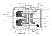
- FIG. 2 is a plan view of the base before mounting the integrated circuit element and the piezoelectric vibration element of FIG. 1 in the first embodiment of the present invention.
- FIG. 2 is a bottom view of the base of FIG. 1 in the first embodiment of the present invention. It is a bottom view of the integrated circuit element applied to this invention.
- FIG. 6 is a bottom view of a base before mounting the integrated circuit element of FIG. 5 in a second embodiment of the present invention. It is a circuit diagram of a piezoelectric oscillator.
- FIG. 1 to 3 show a first embodiment of the present invention
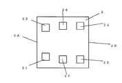
- FIG. 4 is a bottom view of an integrated circuit element applied to the present invention
- 5 and 6 show a second embodiment of the present invention.
- common or corresponding parts are denoted by the same reference numerals.
- the piezoelectric oscillator is applied to a crystal oscillator.
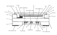
- the crystal oscillator 6 includes a base 1 made of an insulating ceramic multilayer substrate having a recess, an integrated circuit element 2 housed in the base 1, a piezoelectric vibration element 3 housed in the upper part of the base 1, and a base 1. And a lid 4 joined to the opening.
- the base 1 and the lid 4 constitute a package of the crystal oscillator 6.
- the base 1 and the lid 4 are heat-melt bonded using a sealing material 5.
- the piezoelectric vibration element 3 is configured by, for example, an AT-cut quartz crystal vibration plate.
- the inside of the base 1 is hermetically sealed by joining the sealing material 5.
- the first embodiment will be described with reference to FIGS.
- the crystal oscillator 6 only the upper part of the base 1 is open.
- the integrated circuit element 2 is accommodated on the inner bottom surface of the base 1.
- the piezoelectric vibration element 3 is accommodated in the upper part of the base 7.
- the crystal oscillator 6 has a stacked arrangement in which the integrated circuit element 2 and the piezoelectric vibration element 3 are stacked.
- the base 1 is made of a ceramic multilayer substrate and has a rectangular parallelepiped shape as a whole.
- the base 1 is composed of a bottom layer bottom portion 11, an intermediate layer bank portion 12, and a top layer bank portion 13.
- the bottom portion 11 is formed of a single plate having a rectangular shape in a plan view made of an insulating ceramic material such as alumina.
- the bank portion 12 is laminated on the bottom portion 11 and is formed in a frame shape in plan view with a ceramic material.
- the bank portion 13 is formed in a plan view frame shape from a ceramic material.
- the base 1 is formed in a box-like body having a storage portion 10 that is concave when viewed in cross section.
- Embankments 12 and 13 are formed around the storage unit 10.
- the upper surface of the bank portion 13 is formed flat.
- the bank portions 12 and 13 constitute a side wall portion of the base 1.
- the upper surface of the bank portion 13 is the upper end surface of the base 1.
- the storage unit 10 has a rectangular shape in plan view, and includes a first storage unit 10a on the lower side and a second storage unit 10b on the upper side.
- the integrated circuit element 2 is accommodated in the first accommodating portion 10a.
- the piezoelectric vibration element 3 is stored in the second storage portion 10b.
- the base 1 has a three-layer structure including the bottom 11 and the bank portions 12 and 13, but may have a single-layer structure or a two-layer structure depending on the structure of the storage section 10 of the base 1. Four or more layers may be used.
- the upper surface of the bank portion 13 of the base 1 serves as a joining region 13a with the lid 4.
- the junction region 13a is made of a metal film.
- the bonding region 13a is a three-layer metal film including a metallized layer made of a metallized material such as tungsten or molybdenum, a nickel layer stacked on the metallized layer, and a gold layer stacked on the nickel layer. Consists of. Tungsten or molybdenum is integrally formed at the time of ceramic firing by metallization technology using thick film printing technology. A nickel layer and a gold layer are formed on the metallized layer by plating in this order.
- a plurality of castellations C1, C2, C3, and C4 extending in the vertical direction are formed at the four corners of the outer peripheral wall of the base 1.
- circular cutouts are formed in the vertical direction with respect to the outer peripheral wall of the base.
- junction region 13a is formed on the outer bottom surface of the base by at least one of the conductive via V2 penetrating and connecting the base bank portions 12 and 13 and the wiring pattern (not shown) formed above the castellation C2. Electrically derived to the external terminal pad GT2.
- the metal lid 4 When the external terminal pad GT2 is grounded, the metal lid 4 is grounded via the bonding region 13a, the conductive via, the wiring pattern above the castellation, and the like. This grounding provides the electromagnetic shielding effect of the crystal oscillator 6.
- a first storage portion 10 a having a substantially rectangular shape in plan view for storing the integrated circuit element 2 is formed by the bank portion 12.
- the inner side surfaces of the left and right sides of the bank portion 12 project inward from the bank portion 13, and the left projecting portion of the bank portion 12 serves as a holding base 10 c that holds one end of the piezoelectric vibration element 3.
- the protruding portion on the right side in the figure is a pillow portion 10d that faces the holding base 10c via the first storage portion 10a.
- a second storage portion 10b formed by the bank portion 13 is formed above the first storage portion 10a.
- the inner bottom surface 10a1 of the first storage portion 10a has a pair of upper and lower parts in the drawing, the first internal terminal pads NT1, NT2, the second internal terminal pads NT3, NT4, and the third internal terminal pad NT5. , NT6 are juxtaposed in the left-right direction in the figure.
- the first storage portion 10a is formed in a substantially rectangular shape in plan view having two specific sides 101a and 102a parallel to the parallel arrangement direction.
- a plurality of rectangular internal terminal pads NT (NT1 to NT6) connected to the pads of the integrated circuit element 2 are formed on the upper surface of the bottom 11 which is the lowermost layer of the base 1, that is, the inner bottom surface 10a1 of the first storage portion 10a.
- a wiring pattern H (a generic name of H1 to H6 to be described later) extending side by side.
- the internal terminal pad NT two pairs of first internal terminal pads NT1 and NT2 are illustrated for the piezoelectric vibration element 3 in which one is for AC input and the other is for AC output.
- the signal input pad and the signal output pad are electrically connected to each other and are connected to two pairs of first pads 21 and 22 of the integrated circuit element 2.
- One of the first pads 21 and 22 of the integrated circuit element 2 is connected to the signal input pad of the piezoelectric vibration element 3 via one of the first internal terminal pads NT1 and NT2, and the other is the first internal terminal pad NT1.
- NT2 is connected to the signal output pad of the piezoelectric vibration element 3 through the other of NT2.
- Two pairs of second internal terminal pads NT3 and NT4 are used for outputting an AC signal of the integrated circuit element 2 and for the other one for grounding the integrated circuit element 2, and a pair of second pads 23 of the integrated circuit element 2. , 24.
- the second pad 23 of the integrated circuit element 2 is a pad to which an AC signal is output from the integrated circuit element 2, and the output AC signal is output to the second internal terminal pad NT3.
- the two pairs of third internal terminal pads NT5 and NT6 are pads to which a DC potential or a ground potential is applied, and are connected to the two pairs of third pads 25 and 26 of the integrated circuit element 2.
- the DC potential or the ground potential is applied from the integrated circuit element 2.
- the wiring pattern H includes six first to sixth wiring patterns H1 to H6.
- the first wiring patterns H1, H2 extend the first internal terminal pads NT1, NT2, respectively.
- the second wiring patterns H3 and H4 extend the second internal terminal pads NT3 and NT4, respectively.
- Third wiring patterns H5 and H6 extend third internal terminal pads NT5 and NT6, respectively.
- the third internal terminal pad NT5 and the third wiring pattern H5 are formed along the periphery (partial periphery) of the two sides of the first internal terminal pad NT1, and the first internal terminal pad NT1 is formed.
- a third internal terminal pad NT6 and a third wiring pattern H6 are formed along the periphery (partial periphery) of the two sides of the terminal pad NT2.
- the third internal terminal pad NT5 and the third wiring pattern H5, and the third internal terminal pad NT6 and the third wiring pattern H6 are both radiated noise from the second pad 23 of the integrated circuit element 2 due to the first internal terminal pad NT1.
- a conductive path for blocking radiation noise is formed to block the NT2 side from reaching.
- the first internal terminal pads NT1, NT2 and the second internal terminal pads NT3, NT4 are separated from each other with the radiation noise blocking conductive path in between.
- the radiation noise blocking conductive path has a function of blocking radiation noise, a DC potential or a ground potential is applied to the third internal terminal pads NT5 and NT6. This potential is applied from the integrated circuit element 2.
- first internal terminal pads NT1 and NT2 and the second internal terminal pads NT3 and NT4 are more specific to the specific sides 101a and 102a of the first storage portion 10a than the third internal terminal pads NT5 and NT6 positioned therebetween. Widely formed in parallel directions.
- the internal terminal pads NT5 and NT6 are arranged opposite to each other substantially symmetrically.
- the third internal terminal pads NT5 and NT6 are disposed substantially opposite to each other along a virtual line L2 orthogonal to the specific sides 101a and 102a passing through the center point O of the first storage portion 10a.
- NT11 and NT21 which are one side closest to the second internal terminal pads NT3 and NT4 face the external environment.
- the third internal terminal pads NT5 and NT6 are substantially L-shaped and substantially symmetrical with respect to the imaginary line L1 along the periphery of two sides of NT12 and NT22 which are one side closest to the bank portion 12.
- Third wiring patterns H5 and H6 are formed.
- the third internal terminal pad NT5 and the third wiring pattern H5 are substantially L-shaped to form a first radiation noise blocking conductive path surrounding the first internal terminal pad NT1, and the third internal terminal pad.
- NT6 and the third wiring pattern H6 are substantially L-shaped to form a second radiation noise blocking conductive path surrounding the first internal terminal pad NT2.
- the first conductive path is formed along with the formation of each of the conductive paths.
- the first internal terminal pads NT1 and NT2 are securely surrounded by the conductive paths without unnecessarily increasing the area of the storage portion 10a, and the second internal terminal pads NT3 and NT3 are sandwiched between the conductive paths. Can be separated from NT4.
- a plurality of external terminal pads GT connected to external parts and external devices are formed on the bottom surface of the bottom 11 of the base 1. Specifically, as shown in FIG. 3, external terminal pads GT1, GT2, GT3, and GT4 are formed.
- External terminal pads GT1 to GT4 are external wiring patterns formed in conductive vias V1, V2, V3, V4 and castellations C1, C2, C3, C4 that vertically connect the bottom portion 11 of the base 1 (see FIG.
- the second internal terminal pad NT3 and the second wiring pattern H3 are connected to the second pad 23 serving as an AC output of the integrated circuit element 2 and formed on the conductive via V1 or the castellation C1. It is electrically led to the external terminal pad GT1 formed on the base bottom surface side by at least one of the wiring patterns (not shown).
- the external terminal pad GT1 finally becomes an AC output external terminal.
- the holding base 10c on which the piezoelectric vibration element 3 is mounted is formed on the upper surface of the bank portion 12 of the base 1, that is, the inner bottom surface of the second storage portion 10b.
- Fourth internal terminal pads NT7 and NT8 connected to the excitation electrode of the piezoelectric vibration element 3 are formed on the upper surface of the holding table 10c.
- the fourth internal terminal pad NT7 connected to one excitation electrode 31 of the piezoelectric vibration element 3 is electrically derived by the conductive via V5 penetratingly connecting the first wiring pattern H1 and the bank portion 12.
- the second internal terminal pad NT8 connected to the other excitation electrode 32 of the piezoelectric vibration element 3 is electrically derived by the conductive via V6 penetratingly connecting the first wiring pattern H2 and the bank portion 12.
- the base 1 is formed by using a well-known ceramic lamination technique or metallization technique, and each internal terminal pad, external terminal pad, and wiring pattern are made of tungsten in the same manner as the formation technique of the bonding region 13a.
- a nickel plating layer and a gold plating layer are formed on the upper surface of the metallized layer made of molybdenum or the like.
- the integrated circuit element 2 mounted in the first storage unit 10a is a one-chip integrated circuit element incorporating an inverter amplifier (oscillation amplifier) such as a C-MOS, and constitutes an oscillation circuit together with the piezoelectric vibration element 3. .
- an inverter amplifier oscillation amplifier
- the integrated circuit element 2 includes pads 21 to 26 formed in a rectangular shape.
- pads 21 to 26 formed in a rectangular shape.
- two opposing first pads 21 and 22 are formed near the first side 2A of the integrated circuit element.
- the two opposing second pads 23 and 24 are formed closer to the second side 2B facing the first side 2A.
- Two opposing third pads 25 and 26 are formed between the first pad and the second pad, respectively.
- the first pads 21 and 22 are electrically connected to the excitation electrode of the piezoelectric vibration element 3.
- One of the two second pads 23 and 24 serves as an AC output pad of the integrated circuit element 2.
- the integrated circuit element 2 flips the plurality of pads 21 to 26 of the integrated circuit element 2 and the internal terminal pads NT1 to NT6 formed on the base 1 through, for example, metal bumps C such as gold, for example, by ultrasonic thermocompression bonding. Electromechanical bonding is performed by a chip bonding method.
- the piezoelectric vibration element 3 is mounted above the integrated circuit element 2 with a predetermined interval.
- the piezoelectric vibration element 3 is, for example, a rectangular AT-cut crystal diaphragm.
- a pair of rectangular excitation electrodes 31 and 32 and these extraction electrodes are formed facing the front and back surfaces of the piezoelectric vibration element 3.
- These electrodes are, for example, a laminated thin film composed of a chromium or nickel base electrode layer, a silver or gold intermediate electrode layer, and a chromium or nickel upper electrode layer, or a chromium or nickel base electrode layer and And a laminated thin film composed of a silver or gold upper electrode layer.
- Each of these electrodes can be formed by a thin film forming means such as a vacuum deposition method or a sputtering method.
- Bonding of the piezoelectric vibration element 3 and the base 1 is performed using a conductive bonding material, for example, a silicone-based conductive resin adhesive S that is in a paste form and contains metal fine pieces such as a silver filler.
- a conductive bonding material for example, a silicone-based conductive resin adhesive S that is in a paste form and contains metal fine pieces such as a silver filler.
- the conductive resin adhesive S is applied to the upper surfaces of the first internal terminal pads NT7 and the second internal terminal pads NT8, and the one end portion of the piezoelectric vibration element 3 and the holding base 10c. It is cured by interposing. Thereby, the one end part of the piezoelectric vibration element 3 and the holding stand 10c are electrically and mechanically joined. As described above, the piezoelectric vibration element 3 is cantilevered while providing a gap from the inner bottom surface 10 a 1 of the first storage portion 10 a of the base 1.
- the lid 4 that hermetically seals the base 1 is formed by forming a metal brazing material on a core material made of, for example, Kovar.
- the metal brazing material joins the lid 4 and the joining region (metal film) 13 a of the base 1 as the sealing material 5.
- the outline of the lid 4 in plan view is substantially the same as or slightly smaller than the outline of the ceramic base.
- the bonding area 13a of the base 1 in which the integrated circuit element 2 and the piezoelectric vibration element 3 are stored in the storage unit 10 is covered with the lid 4, and the sealing material 5 of the lid 4 and the bonding area 13a of the base are melted.
- the crystal oscillator 6 is completed by being cured and hermetically sealed.
- the crystal oscillator 8 has a base 7 having a recess having both upper and lower portions opened.
- This base 7 has an H-type arrangement in which the integrated circuit element 2 is accommodated on the inner bottom surface of the lower recess and the piezoelectric vibration element 3 is accommodated on the inner bottom surface of the upper recess. 5 and 6, a part of the description of the same parts as those of the first embodiment is omitted.
- the base 7 is made of a ceramic multilayer substrate, and the whole is a rectangular parallelepiped. As shown in FIG. 5, the base 7 is composed of an intermediate plate 71 in the intermediate layer, an upper bank 72, and a lower bank 73.
- the middle plate portion 71 is a single plate formed in a rectangular shape in plan view with an insulating ceramic material such as alumina.
- the bank portion 72 is formed in a frame shape in plan view by a ceramic material laminated on the middle plate portion 71.
- the bank portion 73 is formed in a planar frame shape by a ceramic material laminated under the middle plate portion 71.
- the base 7 is formed in a substantially H-shaped box-like body as seen in a cross section having two first and second storage portions 70a and 70b on the upper and lower sides.
- a bank portion 72 is formed around the storage portion 70a.
- the upper surface of the bank 72 is formed flat.
- a bank portion 73 is formed around the storage portion 70b.
- the lower surface of the bank portion 73 is formed flat.
- the piezoelectric vibration element 3 is stored in the first storage portion 70a.
- the integrated circuit element 2 is stored in the second storage portion 70b.
- the base 7 has a three-layer structure including the intermediate plate portion 71 and the bank portions 72 and 73, but may have four or more layers according to the structure of the base storage portion.
- the upper surface of the bank portion 72 of the base 1 is a joining region 72 a with the lid 4.
- a metal film is formed in the bonding region 72a.
- the metal film is composed of a metallized layer made of a metallized material such as tungsten or molybdenum, a nickel layer laminated on the metallized layer, and a gold layer laminated on the nickel layer.
- Tungsten or molybdenum is integrally formed at the time of ceramic firing by metallization technology using the thick film printing technology, and is formed on the metallization layer by plating in the order of nickel layer and gold layer.
- the castellations C1 to C4 have a configuration in which an arc-shaped cutout is formed in the vertical direction with respect to the outer peripheral wall of the base.
- the joining region 72a is formed on the base bottom side by at least one of a conductive via (not shown) that vertically connects the base bank portion 72 and the middle plate portion 71 and a wiring pattern (not shown) formed above the castellation C2. Is electrically led out to a part of the external terminal pad GT2 formed in the above.
- the metal lid 4 is grounded via the bonding region 72a, the conductive via, the wiring pattern above the castellation, and the like. By this grounding, the electromagnetic shielding effect of the crystal oscillator 8 can be obtained.
- a second storage part 70b having a substantially rectangular shape in plan view for storing the integrated circuit element 2 is formed on the lower surface inside the base 7 by the bank part 73.
- a first storage portion 70 a having a substantially rectangular shape in plan view for storing the piezoelectric vibration element 3 is formed on the upper surface inside the base 7 by the bank portion 72.
- the second storage portion 70b has two specific sides parallel to the direction in which the first internal terminal pads NT1 and NT2, the second internal terminal pads NT3 and NT4, and the third internal terminal pads NT5 and NT6 are arranged in parallel. It is formed in a substantially rectangular shape having 71b and 72b.
- a plurality of rectangular internal terminal pads NT connected to the integrated circuit element 2 and a wiring pattern H extending these are formed side by side.
- the first wiring patterns H1, H2 extending from the first internal terminal pads NT1, NT2 and the second internal terminal pads NT3, NT4, respectively, are extended.
- Second wiring patterns H3 and H4 and third wiring patterns H5 and H6 extending from third internal terminal pads NT5 and NT6, respectively, are formed.
- H5 is formed.
- a third internal terminal pad NT6 and a third wiring pattern H6 extending from the third internal terminal pad NT6 are formed along the periphery (partial periphery) of the two sides of the first internal terminal pad NT2.
- the third wiring pattern H5 and the third internal terminal pad NT5, and the third internal terminal pad NT6 and the third wiring pattern H6 are both radiated noise from the second pad 23 of the integrated circuit element 2 due to the first internal terminal pad NT1.
- a conductive path for blocking radiation noise is formed to block the NT2 side from reaching.
- the first internal terminal pads NT1 and NT2 and the second internal terminal pads NT3 and NT4 are separated from each other with the radiation noise blocking conductive path in between. Thereby, the radiation noise generated from the second pad 23 of the integrated circuit element 2 is suppressed from reaching the first internal terminal pads NT1, NT2.
- the radiation noise blocking conductive path has a function of blocking radiation noise
- a DC potential or a ground potential is applied to the third internal terminal pads NT5 and NT6. This potential is applied from the integrated circuit element 2.
- the first internal terminal pads NT1 and NT2 and the second internal terminal pads NT3 and NT4 are parallel to the specific sides 71b and 72b of the second storage portion 70b from the third internal terminal pads NT5 and NT6 positioned therebetween. Widely formed.
- the two third internal terminal pads NT5 and NT6 are arranged opposite to each other in a substantially symmetrical manner, and the two third internal terminal pads NT5 and NT6 pass through the second storage portion 70b center point O and the specific sides 71b and 72b. Are substantially opposed to each other along a virtual line L2 orthogonal to the line.
- first internal terminal pads NT1 and NT2 formed in a rectangular shape, NT11 and NT21 which are one side closest to the second internal terminal pads NT3 and NT4 and the bank 73 facing the external environment are closest.
- the third internal terminal pads NT5 and NT6 and the third internal terminal pads NT5 and NT6 are substantially L-shaped along the periphery of two sides of NT12 and NT22, which are one side, and substantially symmetrical with respect to the virtual line L1.
- the third internal terminal pad NT5 and the third wiring pattern H5 are substantially L-shaped to form a first radiation noise blocking conductive path surrounding the first internal terminal pad NT1, and the third internal terminal pad.
- NT6 and the third wiring pattern H6 are substantially L-shaped to form a second radiation noise blocking conductive path surrounding the first internal terminal pad NT2.
- the lower surface of the bank portion 73 of the base 7 is flat as described above, and a plurality of external terminal pads GT connected to external parts and external devices are formed.
- the external terminal pads GT1 to GT4 are formed in conductive vias (not shown) penetratingly connected to the upper part or the castellations C1, C2, C3, C4 of the base.
- the second internal terminal pad NT3 and the second wiring pattern H3 are connected to the second pad 23 serving as an AC output of the integrated circuit element 2, and finally connected to the external terminal pad GT1.
- the external terminal pad GT1 is configured as an AC output external terminal.
- the first wiring patterns H1 and H2 are electrically led out to the outside by means of conductive vias (not shown) that penetrate through the intermediate plate portion 71.
- the base 7 configured as described above is formed using a known ceramic lamination technique or metallization technique, and the internal terminal pads, the external terminal pads, and the wiring patterns are made of tungsten or molybdenum in the same manner as in the formation of the bonding region 72a.
- Each of the nickel plating layer and the gold plating layer is formed on the upper surface of the metallized layer.
- the integrated circuit element 2 includes a plurality of pads 21 to 26 of the integrated circuit element 2 and internal terminal pads NT1 to NT6 formed on the base 7 through metal bumps C such as gold. For example, it is joined electromechanically by a flip chip bonding method using ultrasonic thermocompression bonding.
- the piezoelectric vibration element 3 and the base 7 are bonded using a conductive bonding material, for example, a silicone-based conductive resin adhesive S that is a paste and contains metal fine pieces such as a silver filler.
- a conductive bonding material for example, a silicone-based conductive resin adhesive S that is a paste and contains metal fine pieces such as a silver filler.
- the conductive resin adhesive S is applied to the upper surfaces of the first internal terminal pads NT7 and the second internal terminal pads NT8, and the conductive resin adhesive S is attached to the piezoelectric vibration element 3.
- the first and second internal terminal pads NT7 and NT8 and the inner bottom surface 70a1 of the first storage portion 70a are electrically connected by being interposed between the inner bottom surface 70a1 of the first storage portion 70a of the base 7 and cured. It is mechanically joined.
- one end portion of the piezoelectric vibration element 3 is provided with a gap from the inner bottom surface 70a1 of the first storage portion 70a of the base 7, and the other opposite end portion of the piezoelectric vibration element 3 is connected to the first storage portion of the base 7. Joining to the inner bottom surface 70a1 of 70a, the piezoelectric vibration element is cantilevered.
- the lid 4 for hermetically sealing the base 7 is formed by forming a metal brazing material on a core material made of, for example, Kovar.
- the metal brazing material joins the lid 4 and the joining region (metal film) 72 a of the base 1 as the sealing material 5.
- the external shape of the metal lid in plan view is substantially the same as or slightly smaller than that of the ceramic base.
- the integrated circuit element 2 is stored in the second storage portion 70b of the base 7 and the piezoelectric vibration element 3 is stored in the first storage portion 70a.
- the crystal oscillator 8 is completed by covering, melting and hardening the sealing material 5 of the metal lid 4 and the base joining region 72a and hermetically sealing the piezoelectric vibration element 3.
- the third internal terminal pads NT5 and NT6 and the third wiring patterns H5 and H6 are arranged along the periphery (partial periphery) of the two sides of the first internal terminal pads NT1 and NT2.
- the first and second radiation noise blocking conductive paths are formed.
- the displacement of the bumps C with respect to the pads, or the The misalignment between the pad and the internal terminal pad can be absorbed by the wide first internal terminal pads NT1 and NT2 and the second internal terminal pads NT3 and NT4.
- the bump C does not protrude from the internal terminal pads NT1 to NT6 and are not joined. Further, the first internal terminal pads NT1, NT2 and the second internal terminal pads NT3, NT4 are formed wider than the third internal terminal pads NT5, NT6, so that the plane areas are slightly different or the positions of the pads are slightly different. Even different types of integrated circuit elements 2 can be mounted on the same bases 1 and 7. This makes it easy to diversify products and reduce costs as a piezoelectric oscillator.
- the piezoelectric oscillators 6 and 8 are brought close to each other by the distance between the first internal terminal pads NT1 and NT2 and the second internal terminal pads NT3 and NT4. Can be reduced in size. That is, the present invention can simultaneously improve the mountability, the reliability of bonding, and the versatility when the integrated circuit element 2 is flip-chip bonded, while corresponding to the miniaturization of the piezoelectric oscillators 6 and 8.
- the first internal terminal pads NT1 and NT2, the second internal terminal pads NT3 and NT4, and the third internal terminal pads NT5 and NT6 pass through the central point O of the storage portion for the integrated circuit element. Oppositely arranged symmetrically with respect to a virtual line L1 parallel to the specific side.
- the first pads 21 and 22 and the first internal terminals NT1 and NT2, the second pads 23 and 24, and the second are paired with respect to the warp in the direction orthogonal to the specific side of the storage portion for the integrated circuit element.
- the heights of the internal terminals NT3 and NT4 and the third pads 25 and 26 and the third internal terminals NT5 and NT6 due to warpage can be made uniform.
- the internal terminal pads of the bases 1 and 7 and the pads of the integrated circuit element are flip-chip bonded by ultrasonic thermocompression bonding via the bumps, the paired first pads 21 and 22 and the first internal terminals NT1 and NT2, the second pads 23 and 24 and the second internal terminals NT3 and NT4, and the third pads 25 and 26 and the third internal terminals NT5 and NT6 are pressed against the pair of bumps C in a uniform manner. As a result, the strength does not vary.
- the third internal terminal pads NT5 and NT6 are arranged substantially opposite to each other along a virtual line L2 orthogonal to the specific side passing through the center point O of the storage portion for the integrated circuit element.
- a storage portion for the integrated circuit element can be arranged near the apex of the warp in both the specific side direction and the direction orthogonal to the specific side direction (near the central point O in this embodiment).
- the first pads 21 and 22 and the first internal terminals NT1 and NT2, the second pads 23 and 24 and the second internal terminals NT3 and NT4, and the third pads 25 and 26 and the third internal terminal NT5 are paired.
- the pressing force against the bump C and the pressing strength at a total of six locations in NT6 are made uniform.
- the bonding strength is more stable and highly reliable.
- the bonding strength of the bump C when the integrated circuit element 2 is flip-chip bonded is stabilized while corresponding to the miniaturization of the piezoelectric oscillators 6 and 8, and the electromechanical bonding can be performed more reliably. .
- the AT-cut quartz crystal diaphragm is used as the piezoelectric vibrator, but the present invention is not limited to this, and a tuning fork type quartz diaphragm may be used.
- quartz is used as the piezoelectric vibration element
- the present invention is not limited to this, and a piezoelectric single crystal material such as piezoelectric ceramics or LiNbO3 may be used.
- any piezoelectric vibration element can be applied.
- the example in which the piezoelectric vibration element is cantilevered is taken as an example, a configuration in which both ends of the piezoelectric vibration element are retained may be employed.
- a silicone-based conductive resin adhesive is taken as an example of the conductive bonding material, but other conductive resin adhesives may be used.
- a bump material such as a metal bump or a metal plating bump, or a brazing material may be used. Good.
- the present invention uses the piezoelectric vibration element 3 and the integrated circuit element 2, but the present invention is not limited to this.
- the number of piezoelectric vibration elements 3 can be set arbitrarily.
- the crystal oscillator of the H-type arrangement is taken as an example, but only the upper part has a concave part opened, and the integrated circuit element and the piezoelectric vibration element are mounted in parallel with the inner bottom face of the concave part. It can be applied to a crystal oscillator with a flat arrangement.
- the present invention provides a quartz crystal of a heavy box type in which a substrate having a concave portion for an integrated circuit element and a substrate having a concave portion for a piezoelectric vibration element are separately prepared and mounted in a state where they are stacked in the thickness direction. It can also be applied to an oscillator. That is, the member mounted on the base can be set and changed according to the application.
- the electrical connection between the integrated circuit element and the base is not limited to the flip chip bonding method by ultrasonic thermocompression bonding, and other methods may be adopted.
- the present invention is not limited to the above-described oscillation circuit configuration, and may be an oscillation circuit configuration including another oscillation amplifier.
- sealing is not limited to this, and seam sealing, for example, a laser beam or Beam sealing with an electron beam or the like, glass sealing, or the like can also be applied.
- the present invention can be applied to a surface mount type piezoelectric vibration oscillator.
Landscapes
- Physics & Mathematics (AREA)
- Acoustics & Sound (AREA)
- Oscillators With Electromechanical Resonators (AREA)
Abstract
Priority Applications (3)
| Application Number | Priority Date | Filing Date | Title |
|---|---|---|---|
| CN201380005642.4A CN104115395B (zh) | 2012-02-28 | 2013-01-08 | 表面安装型压电振荡器 |
| US14/381,117 US9219217B2 (en) | 2012-02-28 | 2013-01-08 | Surface mount type piezoelectric oscillator |
| JP2014501980A JP6107810B2 (ja) | 2012-02-28 | 2013-01-08 | 表面実装型圧電発振器 |
Applications Claiming Priority (2)
| Application Number | Priority Date | Filing Date | Title |
|---|---|---|---|
| JP2012042175 | 2012-02-28 | ||
| JP2012-042175 | 2012-02-28 |
Publications (1)
| Publication Number | Publication Date |
|---|---|
| WO2013128782A1 true WO2013128782A1 (fr) | 2013-09-06 |
Family
ID=49082001
Family Applications (1)
| Application Number | Title | Priority Date | Filing Date |
|---|---|---|---|
| PCT/JP2013/000008 Ceased WO2013128782A1 (fr) | 2012-02-28 | 2013-01-08 | Oscillateur piézoélectrique du type monté en surface |
Country Status (5)
| Country | Link |
|---|---|
| US (1) | US9219217B2 (fr) |
| JP (1) | JP6107810B2 (fr) |
| CN (1) | CN104115395B (fr) |
| TW (1) | TWI521871B (fr) |
| WO (1) | WO2013128782A1 (fr) |
Cited By (3)
| Publication number | Priority date | Publication date | Assignee | Title |
|---|---|---|---|---|
| JP2015195436A (ja) * | 2014-03-31 | 2015-11-05 | 日本電波工業株式会社 | 電子部品パッケージ及び圧電デバイス |
| JP2016012804A (ja) * | 2014-06-27 | 2016-01-21 | 京セラクリスタルデバイス株式会社 | 恒温槽付圧電デバイス |
| JP2017085450A (ja) * | 2015-10-30 | 2017-05-18 | 日本電波工業株式会社 | リードタイプ水晶発振器 |
Families Citing this family (8)
| Publication number | Priority date | Publication date | Assignee | Title |
|---|---|---|---|---|
| JP6167494B2 (ja) * | 2012-09-26 | 2017-07-26 | セイコーエプソン株式会社 | 電子デバイス用容器の製造方法、電子デバイスの製造方法、電子デバイス、電子機器及び移動体機器 |
| US20150188025A1 (en) * | 2013-12-30 | 2015-07-02 | Nihon Dempa Kogyo Co., Ltd. | Container for electronic component and electronic component |
| TWI610472B (zh) | 2014-05-12 | 2018-01-01 | 松下知識產權經營股份有限公司 | 壓電元件與電纜基板之連接方法、附有電纜基板之壓電元件及使用其之噴墨頭 |
| JP1525432S (fr) * | 2014-09-16 | 2015-06-08 | ||
| USD760230S1 (en) * | 2014-09-16 | 2016-06-28 | Daishinku Corporation | Piezoelectric vibration device |
| JP6666161B2 (ja) * | 2016-01-25 | 2020-03-13 | 日本電波工業株式会社 | 水晶発振器 |
| CN111682097B (zh) * | 2020-06-12 | 2022-05-31 | 瑞声声学科技(深圳)有限公司 | 一种压电结构及压电装置 |
| JP7571637B2 (ja) * | 2021-03-17 | 2024-10-23 | 株式会社大真空 | 恒温槽型圧電発振器 |
Citations (7)
| Publication number | Priority date | Publication date | Assignee | Title |
|---|---|---|---|---|
| JP2001274628A (ja) * | 2000-03-23 | 2001-10-05 | Daishinku Corp | 圧電振動デバイス |
| JP2006191517A (ja) * | 2004-12-07 | 2006-07-20 | Seiko Epson Corp | 温度補償型圧電発振器 |
| JP2009124619A (ja) * | 2007-11-19 | 2009-06-04 | Nippon Dempa Kogyo Co Ltd | 表面実装用の水晶発振器 |
| JP2009141666A (ja) * | 2007-12-06 | 2009-06-25 | Nippon Dempa Kogyo Co Ltd | 表面実装用の水晶発振器 |
| JP2009246696A (ja) * | 2008-03-31 | 2009-10-22 | Nippon Dempa Kogyo Co Ltd | 表面実装用の水晶発振器 |
| JP2010050537A (ja) * | 2008-08-19 | 2010-03-04 | Nippon Dempa Kogyo Co Ltd | 水晶発振器 |
| JP2010119013A (ja) * | 2008-11-14 | 2010-05-27 | Nippon Dempa Kogyo Co Ltd | 表面実装水晶発振器 |
Family Cites Families (19)
| Publication number | Priority date | Publication date | Assignee | Title |
|---|---|---|---|---|
| US6229249B1 (en) * | 1998-08-31 | 2001-05-08 | Kyocera Corporation | Surface-mount type crystal oscillator |
| JP2001291742A (ja) | 2000-04-06 | 2001-10-19 | Nippon Dempa Kogyo Co Ltd | Icチップの接合方法及びこれを用いた水晶発振器 |
| JP4228679B2 (ja) * | 2002-12-11 | 2009-02-25 | エプソントヨコム株式会社 | 圧電発振器 |
| JPWO2004079895A1 (ja) * | 2003-03-06 | 2006-06-08 | 松下電器産業株式会社 | 水晶発振回路 |
| JP4347114B2 (ja) | 2004-03-31 | 2009-10-21 | 日本電波工業株式会社 | 表面実装用の水晶発振器 |
| JP4799984B2 (ja) * | 2005-09-30 | 2011-10-26 | 日本電波工業株式会社 | 表面実装用の温度補償水晶発振器 |
| US7602107B2 (en) * | 2005-11-30 | 2009-10-13 | Nihon Dempa Kogyo Co., Ltd. | Surface mount type crystal oscillator |
| JP2007274339A (ja) | 2006-03-31 | 2007-10-18 | Daishinku Corp | 表面実装型圧電振動デバイス |
| JP5072436B2 (ja) * | 2007-05-22 | 2012-11-14 | 日本電波工業株式会社 | 表面実装用の水晶発振器 |
| JP5084383B2 (ja) * | 2007-07-19 | 2012-11-28 | 日本電波工業株式会社 | 表面実装用の水晶発振器 |
| JP5098668B2 (ja) | 2008-01-25 | 2012-12-12 | 株式会社大真空 | 表面実装型圧電発振器 |
| JP5126679B2 (ja) | 2008-08-20 | 2013-01-23 | 学校法人神奈川大学 | リング発振器 |
| JP5144452B2 (ja) | 2008-09-30 | 2013-02-13 | 京セラクリスタルデバイス株式会社 | 圧電発振器 |
| JP2011193109A (ja) * | 2010-03-12 | 2011-09-29 | Seiko Epson Corp | 電子デバイス |
| CN102918767B (zh) * | 2010-05-28 | 2016-03-30 | 株式会社大真空 | 压电振动器件的密封部件及压电振动器件 |
| WO2011155600A1 (fr) * | 2010-06-11 | 2011-12-15 | 株式会社大真空 | Oscillateur |
| JP5652606B2 (ja) * | 2010-12-03 | 2015-01-14 | セイコーエプソン株式会社 | 弾性表面波共振子、弾性表面波発振器、及び電子機器 |
| JP5757786B2 (ja) * | 2011-01-06 | 2015-07-29 | 日本電波工業株式会社 | 水晶発振器 |
| JP5977021B2 (ja) * | 2011-11-30 | 2016-08-24 | 日本電波工業株式会社 | 表面実装型圧電発振器 |
-
2013
- 2013-01-08 CN CN201380005642.4A patent/CN104115395B/zh active Active
- 2013-01-08 US US14/381,117 patent/US9219217B2/en active Active
- 2013-01-08 WO PCT/JP2013/000008 patent/WO2013128782A1/fr not_active Ceased
- 2013-01-08 JP JP2014501980A patent/JP6107810B2/ja active Active
- 2013-01-15 TW TW102101450A patent/TWI521871B/zh active
Patent Citations (7)
| Publication number | Priority date | Publication date | Assignee | Title |
|---|---|---|---|---|
| JP2001274628A (ja) * | 2000-03-23 | 2001-10-05 | Daishinku Corp | 圧電振動デバイス |
| JP2006191517A (ja) * | 2004-12-07 | 2006-07-20 | Seiko Epson Corp | 温度補償型圧電発振器 |
| JP2009124619A (ja) * | 2007-11-19 | 2009-06-04 | Nippon Dempa Kogyo Co Ltd | 表面実装用の水晶発振器 |
| JP2009141666A (ja) * | 2007-12-06 | 2009-06-25 | Nippon Dempa Kogyo Co Ltd | 表面実装用の水晶発振器 |
| JP2009246696A (ja) * | 2008-03-31 | 2009-10-22 | Nippon Dempa Kogyo Co Ltd | 表面実装用の水晶発振器 |
| JP2010050537A (ja) * | 2008-08-19 | 2010-03-04 | Nippon Dempa Kogyo Co Ltd | 水晶発振器 |
| JP2010119013A (ja) * | 2008-11-14 | 2010-05-27 | Nippon Dempa Kogyo Co Ltd | 表面実装水晶発振器 |
Cited By (3)
| Publication number | Priority date | Publication date | Assignee | Title |
|---|---|---|---|---|
| JP2015195436A (ja) * | 2014-03-31 | 2015-11-05 | 日本電波工業株式会社 | 電子部品パッケージ及び圧電デバイス |
| JP2016012804A (ja) * | 2014-06-27 | 2016-01-21 | 京セラクリスタルデバイス株式会社 | 恒温槽付圧電デバイス |
| JP2017085450A (ja) * | 2015-10-30 | 2017-05-18 | 日本電波工業株式会社 | リードタイプ水晶発振器 |
Also Published As
| Publication number | Publication date |
|---|---|
| CN104115395A (zh) | 2014-10-22 |
| TW201336228A (zh) | 2013-09-01 |
| JPWO2013128782A1 (ja) | 2015-07-30 |
| US9219217B2 (en) | 2015-12-22 |
| CN104115395B (zh) | 2017-06-09 |
| JP6107810B2 (ja) | 2017-04-05 |
| US20150015341A1 (en) | 2015-01-15 |
| TWI521871B (zh) | 2016-02-11 |
Similar Documents
| Publication | Publication Date | Title |
|---|---|---|
| JP6075375B2 (ja) | 表面実装型圧電発振器 | |
| JP6107810B2 (ja) | 表面実装型圧電発振器 | |
| JP4795602B2 (ja) | 発振器 | |
| TWI559583B (zh) | Electronic components for the package and piezoelectric vibration components | |
| JP6020663B2 (ja) | 発振器 | |
| JP2010062959A (ja) | 表面実装型圧電発振器およびその特性測定方法 | |
| JP5910351B2 (ja) | 表面実装型圧電発振器 | |
| JP7605025B2 (ja) | 圧電振動デバイス | |
| JP6098255B2 (ja) | 表面実装型圧電発振器 | |
| JP6131798B2 (ja) | 表面実装型圧電発振器 | |
| JP2014187641A (ja) | 表面実装型圧電発振器 | |
| JP2013239790A (ja) | 表面実装型圧電発振器 | |
| JP2018074350A (ja) | 表面実装型圧電発振器とその回路基板への搭載構造 | |
| JP2013172258A (ja) | 水晶発振器 | |
| JP2013207511A (ja) | 表面実装型圧電発振器 | |
| JP6098224B2 (ja) | 表面実装型圧電発振器 | |
| JP2013207512A (ja) | 表面実装型圧電発振器 | |
| JP6024514B2 (ja) | 表面実装型圧電発振器 | |
| JP2018056668A (ja) | 素子搭載部材及び圧電デバイス | |
| JP2019047308A (ja) | 圧電発振器 | |
| JP2017046265A (ja) | 表面実装型圧電フィルタ | |
| JP2010239328A (ja) | 圧電振動子及び圧電発振器 |
Legal Events
| Date | Code | Title | Description |
|---|---|---|---|
| 121 | Ep: the epo has been informed by wipo that ep was designated in this application |
Ref document number: 13754097 Country of ref document: EP Kind code of ref document: A1 |
|
| ENP | Entry into the national phase |
Ref document number: 2014501980 Country of ref document: JP Kind code of ref document: A |
|
| WWE | Wipo information: entry into national phase |
Ref document number: 14381117 Country of ref document: US |
|
| NENP | Non-entry into the national phase |
Ref country code: DE |
|
| 122 | Ep: pct application non-entry in european phase |
Ref document number: 13754097 Country of ref document: EP Kind code of ref document: A1 |