WO2013129148A1 - Dispositif de mesure des dimensions d'un motif, dispositif à faisceau de particules chargées et programme informatique - Google Patents
Dispositif de mesure des dimensions d'un motif, dispositif à faisceau de particules chargées et programme informatique Download PDFInfo
- Publication number
- WO2013129148A1 WO2013129148A1 PCT/JP2013/053787 JP2013053787W WO2013129148A1 WO 2013129148 A1 WO2013129148 A1 WO 2013129148A1 JP 2013053787 W JP2013053787 W JP 2013053787W WO 2013129148 A1 WO2013129148 A1 WO 2013129148A1
- Authority
- WO
- WIPO (PCT)
- Prior art keywords
- pattern
- image
- charged particle
- particle beam
- distance
- Prior art date
- Legal status (The legal status is an assumption and is not a legal conclusion. Google has not performed a legal analysis and makes no representation as to the accuracy of the status listed.)
- Ceased
Links
Images






Classifications
-
- H—ELECTRICITY
- H01—ELECTRIC ELEMENTS
- H01J—ELECTRIC DISCHARGE TUBES OR DISCHARGE LAMPS
- H01J37/00—Discharge tubes with provision for introducing objects or material to be exposed to the discharge, e.g. for the purpose of examination or processing thereof
- H01J37/26—Electron or ion microscopes; Electron or ion diffraction tubes
- H01J37/261—Details
- H01J37/265—Controlling the tube; circuit arrangements adapted to a particular application not otherwise provided, e.g. bright-field-dark-field illumination
-
- H—ELECTRICITY
- H01—ELECTRIC ELEMENTS
- H01J—ELECTRIC DISCHARGE TUBES OR DISCHARGE LAMPS
- H01J37/00—Discharge tubes with provision for introducing objects or material to be exposed to the discharge, e.g. for the purpose of examination or processing thereof
- H01J37/02—Details
- H01J37/22—Optical, image processing or photographic arrangements associated with the tube
- H01J37/222—Image processing arrangements associated with the tube
-
- H—ELECTRICITY
- H01—ELECTRIC ELEMENTS
- H01J—ELECTRIC DISCHARGE TUBES OR DISCHARGE LAMPS
- H01J37/00—Discharge tubes with provision for introducing objects or material to be exposed to the discharge, e.g. for the purpose of examination or processing thereof
- H01J37/26—Electron or ion microscopes; Electron or ion diffraction tubes
- H01J37/28—Electron or ion microscopes; Electron or ion diffraction tubes with scanning beams
-
- H—ELECTRICITY
- H01—ELECTRIC ELEMENTS
- H01J—ELECTRIC DISCHARGE TUBES OR DISCHARGE LAMPS
- H01J2237/00—Discharge tubes exposing object to beam, e.g. for analysis treatment, etching, imaging
- H01J2237/245—Detection characterised by the variable being measured
- H01J2237/24571—Measurements of non-electric or non-magnetic variables
- H01J2237/24578—Spatial variables, e.g. position, distance
-
- H—ELECTRICITY
- H01—ELECTRIC ELEMENTS
- H01J—ELECTRIC DISCHARGE TUBES OR DISCHARGE LAMPS
- H01J2237/00—Discharge tubes exposing object to beam, e.g. for analysis treatment, etching, imaging
- H01J2237/26—Electron or ion microscopes
- H01J2237/28—Scanning microscopes
- H01J2237/2803—Scanning microscopes characterised by the imaging method
- H01J2237/2806—Secondary charged particle
-
- H—ELECTRICITY
- H01—ELECTRIC ELEMENTS
- H01J—ELECTRIC DISCHARGE TUBES OR DISCHARGE LAMPS
- H01J2237/00—Discharge tubes exposing object to beam, e.g. for analysis treatment, etching, imaging
- H01J2237/26—Electron or ion microscopes
- H01J2237/28—Scanning microscopes
- H01J2237/2809—Scanning microscopes characterised by the imaging problems involved
-
- H—ELECTRICITY
- H01—ELECTRIC ELEMENTS
- H01J—ELECTRIC DISCHARGE TUBES OR DISCHARGE LAMPS
- H01J2237/00—Discharge tubes exposing object to beam, e.g. for analysis treatment, etching, imaging
- H01J2237/26—Electron or ion microscopes
- H01J2237/28—Scanning microscopes
- H01J2237/2813—Scanning microscopes characterised by the application
- H01J2237/2817—Pattern inspection
Definitions
- the present invention relates to a pattern dimension apparatus and a computer program, and more particularly to a pattern dimension measurement apparatus and a computer program for measuring a distance between a plurality of patterns.
- a scanning electron microscope which is one of charged particle beam devices, detects electrons obtained by scanning an electron beam on a sample, and displays a signal based on the detected electrons on a screen in synchronization with the scanning of the electron beam.
- This is an apparatus for obtaining a magnified image of a minute observation object by displaying.
- Many observation objects are very fine, and it is very difficult to find a field of view for scanning an electron beam from a relatively large area with respect to the observation object. Therefore, a method is used in which a reference pattern for visual field position search is provided, the visual field is once aligned with the reference pattern, and then the visual field is positioned on a target observation target.
- Patent Document 1 discloses that a plurality of alignment mark images provided on a die are acquired and a deviation from the center coordinate of the alignment mark image is used as a coordinate correction value.
- Patent Document 2 two different scanned images including the same mark in the operation image are acquired, and the two scanned images are acquired within the same scanning period, and the mark positions in the two scanned images are compared. Thus, it is disclosed that a positional deviation between scanned images is obtained.
- Patent Document 3 discloses that two scanning signal images are acquired, the amount of deviation is calculated by pattern matching between the two images, and the automatic axial adjustment of the electronic lens is performed.
- Patent Document 4 when acquiring a reference image for drift detection, images with different image shift amounts are also acquired at the same time, image shift sensitivity is measured as needed, and drift amount detection is performed according to the reference image and image shift sensitivity. It is disclosed to perform image shift control (drift correction).
- JP 2010-073703 (corresponding US Patent Publication US2011 / 0133066) JP 2011-008968 A JP 2007-194060 A JP 2006-173038 A (corresponding US Patent Publication US 2006/0219907)
- an apparatus for measuring the size of a fine pattern using a scanning electron microscope or the like is required to cope with various measurements due to the diversification of the structure of semiconductor devices and the diversification of process management methods. It has become like this. For example, due to the diversification of pattern shapes, patterns with poor edges serving as measurement standards have come to be scattered.
- One technique for measuring pattern dimensions is to perform dimension measurement by creating a luminance profile by averaging the luminance signals in the direction perpendicular to the measurement direction. When performing this measurement, it is necessary to set a measurement box for extracting the luminance signal.
- the shape of the edge portion is complicated, it is difficult to find a reference position, and as a result, measurement becomes difficult. There is a case.
- the following proposes a pattern dimension measuring device and a computer program for realizing high-precision measurement of patterns that are difficult to set up in a measurement box and between spaced patterns.
- the field of view is moved based on the first distance information determined in advance with the first pattern as a reference, the first image is obtained, and the first image is used for matching.
- Template matching is performed using the template, and based on the second distance information obtained by the template matching and the first distance information, the second pattern included in the first image and the first
- a pattern dimension measuring device and a computer program for calculating the distance to the pattern are proposed.
- a dimension between a reference pattern and a different pattern is obtained when the charged particle beam is deflected from the reference pattern to the different pattern and the different pattern is scanned.
- a charged particle beam apparatus including a calculation unit that corrects based on a deviation in deflection amount obtained based on pattern matching using an image obtained will be described.
- SEM scanning electron microscope
- the flowchart which shows the process of calculating
- the figure which shows the principle of the method of measuring the dimension between patterns based on the beam matching and the pattern matching in a high magnification image The figure which shows the principle of the measuring method which measures the dimension between two different patterns by including a common reference pattern in two visual fields.
- the embodiments described below relate to a method and apparatus suitable for measuring the distance between arbitrary patterns with high accuracy, and a computer program for causing a computer to execute the measurement.
- a sample surface analyzer that scans the surface with a charged particle beam probe and analyzes the quantity or energy of the emitted secondary electrons, ions, electromagnetic waves, and other signals to analyze the surface properties.
- a scanning electron microscope (SEM) that obtains a surface shape image by converting the amount of secondary electrons into luminance on the screen using electrons as probes and secondary electrons as emission signals, in particular, has fine pattern dimensions. Measurement and inspection can be performed.
- signal electrons with low energy that are emitted when an electron beam reaches the sample and excites atoms on the sample surface are called secondary electrons.
- an electron beam is applied to the edge of a sample with irregularities such as a semiconductor circuit pattern, the amount of secondary electrons generated by the edge effect increases, and an image with a contrast depending on the irregularities is formed.
- electrons that rebound on the sample surface without the electron beam reaching the sample are called reflected electrons (or backscattered electrons).
- the reflected electrons are high-energy signal electrons, and an image having a contrast depending on the sample composition is formed without depending on the unevenness of the sample.
- a reflected electron signal is detected in a magnetic head having a flat sample surface or a semiconductor sample that is difficult to observe with a secondary electron signal due to partial charging, and a clear image can be obtained.
- a two-dimensional image reflecting the surface shape of the sample can be acquired. Further, the shape and dimensions of the pattern can be measured based on the detected signal.
- CD-SEM Cross Dimension SEM
- CD-SEM Cross Dimension SEM
- the demand for processing dimensions in manufacturing has become more and more severe, and the precision in dimension measurement has also been severely demanded.
- demands for measurement are diversified.
- the layout of the measurement box may be difficult due to the complexity of the pattern shape itself.
- a wide range of pattern shape measurement is required by exposure simulation, and the conventional methods acquire images at a low magnification, and the measurement accuracy may not meet the requirements.
- it is necessary to manage the pattern arrangement of lithography, and measurement of the distance between patterns with high accuracy is also required.
- the following is a specific example of a dimension measuring apparatus that performs dimension measurement with high accuracy by combining dimension measurement based on beam deflection and dimension measurement based on high-magnification image matching, and a computer program that causes a computer to execute the dimension measurement.
- a dimension measuring apparatus that performs dimension measurement with high accuracy by combining dimension measurement based on beam deflection and dimension measurement based on high-magnification image matching, and a computer program that causes a computer to execute the dimension measurement.
- each pattern is acquired at a high magnification including a certain reference point, and the pattern to be measured and the beam deflection amount from the reference point are recorded. Then, pattern matching with pre-registered model data is performed, the deviation of the deflection amount is corrected at the sub-pixel level, and the distance between the measurement patterns is obtained with high accuracy.
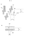
- FIG. 2A shows a pattern of a semiconductor device sample
- FIG. 2B shows an example of a pattern formed on a magnetic head.
- the pattern described below is an example, and the present invention is not limited to this.
- a contact hole pattern 202 is arranged on the right side of several line patterns 201.
- the line pattern 201 and the hole pattern have respective exposure intensity distributions.
- a two-dimensional Gaussian distribution is shown as the intensity distributions 203 and 204.
- the intensity distributions 203 and 204 For example, when the distance between the line pattern 201 and the hole pattern 202 is short, there is a possibility that the two will be short-circuited. This is because the exposure intensities of the overlapping portions increase when the bottoms of the intensity distributions 203 and 204 overlap.
- it is desirable that the number of patterns per unit area is large. Therefore, it is necessary to strictly manage the arrangement interval while arranging a plurality of patterns within a limited range.
- one of the measurement target patterns is a circular pattern
- it is conceivable to set a measurement box according to the pattern shape it is necessary to prepare measurement boxes according to various pattern shapes due to the recent miniaturization and complexity of patterns, which is difficult in reality. is there.
- FIG. 2B is a diagram showing an outline of the magnetic head.
- the magnetic head needs to have the writing unit 205 and the reading unit 206 of the magnetic head patterned at appropriate positions. That is, in order to properly manage the magnetic head, it is necessary to accurately measure these two distances. However, since it is difficult to arrange the measurement boxes and the distance between them is large, the writing unit 205 and the reading unit 206 are accommodated in one high magnification image in one high magnification image. It is difficult.
- each pattern is acquired at a high magnification including a certain reference point, and the pattern to be measured and the beam deflection amount from the reference point are recorded.
- An example will be described in which pattern matching with pre-registered model data is performed, the deviation of the deflection amount is corrected at the sub-pixel level, and the distance between the measurement patterns is obtained with high accuracy.
- the SEM, a control device mounted on the SEM, or a control device connected to the SEM via a communication line or the like will be described as an example.
- the present invention is not limited to this.
- the measurement process may be performed using a general-purpose arithmetic device according to a program.
- the present invention can also be applied to a case where a sample is observed and measured by another charged particle beam apparatus such as a focused ion beam apparatus.
- FIG. 1 is a schematic configuration diagram of a scanning electron microscope (SEM).
- SEM scanning electron microscope
- the retarding voltage is a negative voltage applied to the sample 107 (sample holder 108 or sample stage 109) side in order to converge the electron beam 102 without damaging the circuit pattern on the sample 107.
- the irradiation energy of the electron beam 102 is controlled.
- the generated reflected electrons 111 and secondary electrons 112 collide with the reflector 113 to generate new electrons, and the new electrons are detected by the detector 114.
- the detector 114 has a built-in photomultiplier tube, which generates a voltage according to the detected amount of electrons.
- the signal processing device 115 After this is processed by the signal processing device 115, it is displayed on the image display unit 116 as an image.
- the signal processing device 115 forms a profile waveform with the vertical axis representing the signal amount and the horizontal axis representing the scanning position of the electron beam based on secondary electrons emitted from the sample. Then, the pattern dimension is measured by obtaining the distance between the peaks of the profile waveform.
- secondary electrons are low energy signal electrons of less than about 50 eV and reflected electrons are high energy signal electrons of about 50 eV or more, these are controlled by controlling the voltage and other optical parameters applied to each electrode constituting the SEM.
- the signal detection can be selected and switched between them.
- the above conditions are set in (1) the electron optical system and / or (2) the electron detection system.
- an incident is obtained by subtracting a negative voltage (such as a retarding voltage Vr) for decelerating from a positive acceleration voltage Va for accelerating the electron beam 102 irradiated from the electron gun 101 toward the sample 107 side.
- a negative voltage such as a retarding voltage Vr
- Va positive acceleration voltage
- Va positive acceleration voltage
- Va positive acceleration voltage
- Va positive acceleration voltage
- Va positive acceleration voltage
- Va positive acceleration voltage
- FIG. 8 shows the basic structure of the energy filter.
- the energy filter includes two shield meshes 801a and a filter mesh 801b. These meshes are provided with openings 802 for allowing the electron beam 102 to pass therethrough.
- One or more filter meshes 801a may be provided, and a power source 803 for applying a filter voltage is connected.
- the reflected electrons 111 and the secondary electrons 112 separated according to the magnitude of energy are detected by the reflected electron detector 804a and the secondary electron detector 804b, respectively.
- each detector can detect the electrons separated in accordance with the energy, the resolution becomes high.
- the methods (1) and (2) can be appropriately combined depending on the purpose and application, such as a semiconductor device pattern having irregularities and a flat magnetic head pattern.
- the switching of the electron optical system can guarantee an accurate measurement value by calibrating the apparatus in advance.
- the present embodiment is not limited to the above (1) and (2), and other optical parameters such as voltage and current applied to or supplied to other electrodes and coils constituting the SEM are controlled.
- other optical parameters such as voltage and current applied to or supplied to other electrodes and coils constituting the SEM are controlled.
- it is possible to set signal detection optical conditions for the reflected electrons 111 and the secondary electrons 112.
- the control device includes an arithmetic device, and the arithmetic device controls the device based on an SEM operation program called a recipe.
- FIG. 9 is a schematic configuration diagram of a semiconductor measurement / inspection system including an SEM.
- the system includes an SEM main body 901, an A / D converter 903, and a control device 904.
- the SEM main body 901 irradiates a sample such as a semiconductor wafer with an electron beam, captures electrons emitted from the sample with a detector 902, and converts them into a digital signal with an A / D converter 903.
- the digital signal is input to the control device 904 and stored in the memory 906, and image processing according to the purpose is performed by image processing hardware such as a CPU imaged in the arithmetic device 905 having various functions.
- the arithmetic device 905 also has a function of creating a line profile based on the detection signal and measuring a dimension between peaks of the profile.
- control device 904 is connected to an input device 907 having an input means, and an image or measurement result is displayed to the operator on a display device provided in the input device 907 or an external display (not shown). It has functions such as GUI (Graphical User Interface) to display.
- GUI Graphic User Interface
- control and processing in the control device 904 can be assigned to a CPU or an electronic computer equipped with a memory capable of storing images and processed and controlled. Further, the control device 904 reads out an imaging recipe including the coordinates of an electronic device required for measurement, a pattern matching template used for positioning, imaging conditions, or the like, or reads the recipe manually or electronic device It is also possible to connect via a network or the like to an imaging recipe creation device created by utilizing the design data.
- FIG. 3A is a schematic sectional view of electron beam deflection on the sample.
- a width L when the electron beam 301 is deflected from a certain pattern 302 to a pattern 303 is set.
- FIG. 3B shows the positional relationship of lenses, deflectors, scanning coils, etc. in the SEM electron optical system. After passing through the objective aperture hole 304, the electron beam 301 is converged on the condenser lens 305 and scanned on the sample surface 308.
- the electron beam is changed to a designated place with a certain width, and scanned at a designated magnification to acquire an image. adjust.
- the beam deflection is called image shift, and the image shift X / Y coil control operation amount IS (X) (LSB), IS (Y) (LSB) and the image shift actual operation amount, that is, the physical movement distance (L def (X) ( ⁇ m) and L def (Y) ( ⁇ m) are expressed by the relational expressions (1) and (2) as follows.
- IS (X) (LSB) A * L def (X) ( ⁇ m) + B * L def (Y) ( ⁇ m) (1)
- IS (Y) (LSB) C * L def (X) ( ⁇ m) + D * L def (Y) ( ⁇ m) (2)
- A, B, C, and D are predetermined coefficients for correcting beam deflection and beam rotation at the time of beam deflection. Calibration is performed using a pattern in which a fixed distance is known in advance when adjusting the apparatus, and the deflection control operation amount and actual deflection are calculated. Has a physical distance correction table. Therefore, the physical movement distances L def (X) and L def (Y) can be obtained by back calculation using the above equations (1) and (2) from the control deflection amount of the image shift at the actual measurement length.
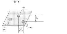
- Fig. 4 explains the principle of high-precision measurement between arbitrary patterns. Patterns 401 and 402 to be measured are arranged on the sample, and distances Lx and Ly between the two patterns are obtained. It is difficult to obtain a pattern dimension by waveform processing by detecting a line profile by placing a conventional rectangular measurement box in which the pattern shape is different from lines and holes.
- the present embodiment provides a method for solving the measurement arrangement problem of an arbitrary pattern and the compatibility between high magnification and a wide range of measurement accuracy.
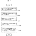
- a specific flow of distance measurement between arbitrary patterns by beam deflection and pattern matching will be described with reference to FIG.
- the stage is controlled to move to a reference point pattern 403 in the vicinity of the patterns 401 and 402 to be measured.
- the beams are deflected from the reference point 403 to the patterns 401 and 402, respectively, and high-magnification SEM images of the respective patterns are acquired (S701).
- control amount (LSB unit) when the beam is deflected is read from the control system, and the actual deflection distance, that is, the pattern distance from the reference point ( ⁇ m unit) L def using the above equations (1) and (2).
- X1, Y1) pattern 401-pattern 403
- L def X2, Y2
- the distance between the patterns 401 and 402 can be calculated once (S702), but the positioning accuracy of the beam deflection is limited to the performance of electrical control, and is about several tens of nanometers. The measurement accuracy is still insufficient for the sub-nm level.
- S703-705 the deviation of the beam deflection is corrected by the SEM image processing of each pattern at the high magnification, and the deviation accuracy is absorbed to achieve sub-nm level measurement accuracy.
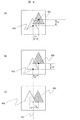
- FIG. 5 shows an example of image matching.
- An image acquired at a high magnification at the deflection destination from the reference point is matched with an image registered in advance (S703).
- the pattern 401 is acquired as an SEM image 502.
- a positional deviation from the previously registered image 503 occurs due to the deviation of the deflection amount.
- the amount of misalignment can be calculated by pattern matching, and there are various image matching techniques. Several examples will be described in the next section.
- the respective centroids of the 502 and 503 patterns are calculated, the position difference between the centroids is derived, the image processing pixel unit is converted to ⁇ m units, and the deviation of the image, that is, the error correction amount L mtchg ( X1, Y1) (pattern 401- pattern 403) and L mtchg (X2, Y2) (pattern 402-pattern 403) are obtained.
- L ptrn (X1, Y1) L mtchg (X1, Y1) + L def (X1, Y1) (3)
- L ptrn (X2, Y2) L mtchg (X2, Y2) + L def (X2, Y2) (4)
- the pixel unit is converted to ⁇ m unit by the following formula (6).
- the error in performing image matching varies slightly depending on the method, accuracy up to the sub-pixel level can be obtained by performing image matching using the above method.
- the SEM magnification is 100 k
- the image scan pixel is 1024
- the image size is 135 mm
- the size corresponding to one pixel is 135 mm / (1024 ⁇ 100 k) to 1.3 nm. Therefore, if the deviation of the deflection amount is corrected by image matching of about sub-pixels, it is possible to achieve distance measurement accuracy with a high accuracy of the number of zeros.
- the accuracy can be maintained by acquiring and measuring a high-magnification image for each pattern instead of a low magnification.
- the box arrangement of the conventional measurement method is unnecessary. Therefore, any pattern different from lines and holes can be measured by performing registration processing and image processing.
- the pattern described here is an example, and the present invention is not limited to this.
- 401 is described as a reference point
- 402 and 403 are measurement target patterns.
- distance measurement of 402 to 403 is also possible using the measurement target pattern 402 itself as a reference pattern.
- the distance measurement of two patterns has been described as an example, a plurality of patterns can be similarly developed, and the distance between each pattern can be measured. In the case of a plurality of patterns, it is also possible to average the measurement of similar patterns and further improve the measurement accuracy by N times.
- Differences in beam deflection due to switching of magnification during measurement, switching of electro-optic mode, and difference in scanning width of SEM images are calibrated in advance using the same standard sample when adjusting the device. Can be evaluated with the same criteria.
- an easily charged sample such as an insulator
- the measurement accuracy of misalignment due to image drift deteriorates, but it is effective to maintain the measurement accuracy of this method by suppressing the image drift due to switching of the electron optical system corresponding to the insulator.
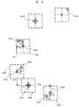
- FIG. 10 is a diagram for explaining an example in which the dimension between the surrounding measurement target patterns or between the reference pattern and the measurement target pattern is measured using the addressing pattern 1001.
- the dimensions between the triangular pattern 1002 and the square pattern 1003 can be measured using the addressing pattern 1001 in the same manner as in the first embodiment.
- from predetermined beam deflection amounts ( ⁇ x1, ⁇ y1) and ( ⁇ x2, ⁇ y2) and deviation amounts ( ⁇ x3, ⁇ y3) and ( ⁇ x4, ⁇ y4) obtained based on pattern matching in the high magnification images 1006, 1007.
- the dimensions ⁇ xs and ⁇ ys between the triangular pattern 1002 and the square pattern 1003 can be obtained as follows.
- Positions 1004 and 1005 are deflection target positions based on the addressing pattern 1001. Further, with the position 1004 as a reference, the beam is deflected by a deflection amount ( ⁇ x5, ⁇ y5), and a deviation amount ( ⁇ x6, ⁇ y6) between the position 1010 and the round pattern 1009 is obtained, thereby obtaining a triangular pattern 1002 and a circle. The distance to the pattern 1009 can also be obtained. In this way, not only between the addressing pattern and the fine pattern, but also application to dimension measurement between the fine patterns is possible.
- the stage is moved, and then the addressing pattern 1012 is searched for. Then, the dimensions between the addressing pattern 1012 and the round pattern 1009 and the addressing pattern in the same manner as in the above embodiment. If the dimension between 1012 and the diamond pattern 1013 is obtained, the dimension between the square pattern 1003 and the diamond pattern 1013 can be obtained. In this case, since the position of the common pattern (round pattern 1009) is specified using the two addressing patterns 1001 and 1012 before and after the stage movement, even between the patterns that are separated by the stage movement, Highly accurate measurement can be performed.
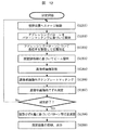
- FIG. 12 is a flowchart showing a process for measuring a dimension between two patterns with stage movement with high accuracy.
- the stage is moved to position the beam irradiation position in the visual field region including the first pattern to be measured and the addressing pattern (step 1201).
- pattern matching is executed to search for addressing pattern data (step 1202).
- the image is acquired with a narrower field of view than the image for searching the addressing pattern.
- the reference position for example, the image center position
- the exact position of the addressing pattern is specified (step 1203).
- an image 1008 having a field of view having the same size as the measurement target pattern is acquired.
- the difference data may be superimposed on the beam deflection amount ( ⁇ x1, ⁇ y1) to obtain the distance between the addressing pattern and the measurement target.
- the beam is deflected based on distance information between the addressing pattern registered in advance and the measurement target pattern or deflection signal information (step 1204).
- a high-magnification image an image with a high magnification relative to the image used at the time of addressing in step 1202 is acquired at this deflection destination (step 1205).
- Template matching is performed in the high-magnification image acquired in this way (step 1207), and the deviation is measured based on the difference between the matching position and the reference position (step 1207).
- the dimensions between the separated patterns are calculated by adding the obtained dimensions between the patterns (step 1208), and the measurement results are registered or displayed. (Step 1209). If acquisition of necessary data has not been completed, the stage is moved to acquire an image including another addressing pattern or another measurement target pattern, and the steps 1202 to 1207 are repeated. .
- the measurement apparatus that performs the measurement process as described above or the computer program that causes the computer to perform the above measurement, it is possible to measure the dimension between the separated patterns with stage movement with high accuracy.
- Electron gun 102 Primary electron beam 103 Accelerating electrodes 104 and 305 Condenser lenses 105 and 306 Deflectors 106 and 307 Objective lens 107 Sample 108 Sample holder 109 Sample stage 110 Booster electrode 111 Reflected electrons 112 Secondary electrons 113 Reflectors 114 and 902 Detection Instrument 115 Signal processor 116 Image display unit 117 Conversion electrode 201, 202, 205, 206 Pattern 203, 204 Pattern intensity distribution 207 Conventional measurement arrangement box 301 Electron beam 302, 303, 401, 402, 502, 605 Sample image formation pattern 304 Objective aperture 403 Reference point pattern 501 Image field 503 Pre-registered model patterns 601 and 602 Sample formation image pattern centroids 603 and 604 Sample formation image pattern bottom midpoint 606 Sample formation Pattern 607 in which image pattern is folded symmetrically Axis of symmetry 801a Shield mesh 801b Filter mesh 802 Opening 803 Power source 804a Reflected electron detector 804b Secondary electron detector 901 SEM main
Landscapes
- Chemical & Material Sciences (AREA)
- Analytical Chemistry (AREA)
- Engineering & Computer Science (AREA)
- Computer Vision & Pattern Recognition (AREA)
- Length-Measuring Devices Using Wave Or Particle Radiation (AREA)
Abstract
La présente invention concerne un dispositif de mesure des dimensions d'un motif qui est capable de mesurer avec une grande précision les dimensions de motifs avec lesquels il est difficile d'installer des boîtes de mesure, et les dimensions se trouvant entre des motifs séparés. Pour ce faire, le dispositif de l'invention : déplace le champ visuel sur la base de premières informations de distance préétablies, en utilisant un premier motif comme référence ; obtient une première image ; effectue un appariement par forme de référence au moyen de la première image et d'une forme de référence pour appariement ; et calcule la distance entre un second motif inclus dans la première image et le premier motif, sur la base de secondes informations de distance obtenues par l'appariement par forme de référence et des premières informations de distance.
Priority Applications (1)
| Application Number | Priority Date | Filing Date | Title |
|---|---|---|---|
| US14/379,659 US9136089B2 (en) | 2012-02-28 | 2013-02-18 | Pattern dimension measuring device, charged particle beam apparatus, and computer program |
Applications Claiming Priority (2)
| Application Number | Priority Date | Filing Date | Title |
|---|---|---|---|
| JP2012040869A JP5941704B2 (ja) | 2012-02-28 | 2012-02-28 | パターン寸法測定装置、及びコンピュータプログラム |
| JP2012-040869 | 2012-02-28 |
Publications (1)
| Publication Number | Publication Date |
|---|---|
| WO2013129148A1 true WO2013129148A1 (fr) | 2013-09-06 |
Family
ID=49082349
Family Applications (1)
| Application Number | Title | Priority Date | Filing Date |
|---|---|---|---|
| PCT/JP2013/053787 Ceased WO2013129148A1 (fr) | 2012-02-28 | 2013-02-18 | Dispositif de mesure des dimensions d'un motif, dispositif à faisceau de particules chargées et programme informatique |
Country Status (3)
| Country | Link |
|---|---|
| US (1) | US9136089B2 (fr) |
| JP (1) | JP5941704B2 (fr) |
| WO (1) | WO2013129148A1 (fr) |
Cited By (4)
| Publication number | Priority date | Publication date | Assignee | Title |
|---|---|---|---|---|
| EP3021280A1 (fr) * | 2014-11-07 | 2016-05-18 | JEOL Ltd. | Procédé d'évaluation d'image et dispositif à faisceau de particules chargées |
| US20190017817A1 (en) * | 2016-01-29 | 2019-01-17 | Hitachi High-Technologies Corporation | Overlay Error Measurement Device and Computer Program |
| JP2023178358A (ja) * | 2018-10-02 | 2023-12-14 | 株式会社ホロン | 電子ビーム測定装置および電子ビーム測定方法 |
| CN117981040A (zh) * | 2021-10-13 | 2024-05-03 | Ict半导体集成电路测试有限公司 | 确定聚焦带电粒子束的束汇聚度的方法和带电粒子束系统 |
Families Citing this family (18)
| Publication number | Priority date | Publication date | Assignee | Title |
|---|---|---|---|---|
| JP6226781B2 (ja) * | 2013-03-27 | 2017-11-08 | 株式会社日立ハイテクサイエンス | 集束イオンビーム装置、それを用いた試料の加工方法、及び集束イオンビーム加工用コンピュータプログラム |
| JP2016058637A (ja) * | 2014-09-11 | 2016-04-21 | 株式会社日立ハイテクノロジーズ | オーバーレイ計測方法、装置、および表示装置 |
| US10312053B2 (en) | 2015-03-31 | 2019-06-04 | Hitachi High-Technologies Corporation | Charged particle beam apparatus, alignment method of charged particle beam apparatus, alignment program, and storage medium |
| JP2017032365A (ja) * | 2015-07-31 | 2017-02-09 | 株式会社日立ハイテクノロジーズ | パターンの計測方法および計測装置 |
| KR101752801B1 (ko) * | 2015-09-10 | 2017-06-30 | 주식회사 포스코 | 치수측정장치 및 방법 |
| JP2017084483A (ja) * | 2015-10-23 | 2017-05-18 | 日本電子株式会社 | キャリブレーション方法および荷電粒子線装置 |
| JP6925783B2 (ja) * | 2016-05-26 | 2021-08-25 | 株式会社アドテックエンジニアリング | パターン描画装置及びパターン描画方法 |
| GB201609995D0 (en) * | 2016-06-08 | 2016-07-20 | Aquasium Technology Ltd | Shaped welding head |
| US10296702B2 (en) | 2017-03-15 | 2019-05-21 | Applied Materials Israel Ltd. | Method of performing metrology operations and system thereof |
| US10120973B2 (en) | 2017-03-15 | 2018-11-06 | Applied Materials Israel Ltd. | Method of performing metrology operations and system thereof |
| JP6850234B2 (ja) * | 2017-09-29 | 2021-03-31 | 株式会社日立ハイテク | 荷電粒子線装置 |
| US11353798B2 (en) * | 2017-10-13 | 2022-06-07 | Hitachi High-Technologies Corporation | Pattern measurement device and pattern measurement method |
| JP7360978B2 (ja) * | 2020-03-18 | 2023-10-13 | 株式会社日立ハイテクサイエンス | 荷電粒子ビーム装置 |
| WO2021199183A1 (fr) * | 2020-03-30 | 2021-10-07 | 株式会社日立ハイテク | Appareil à faisceau de particules chargées et procédé de calcul d'indice de rugosité |
| US11094499B1 (en) * | 2020-10-04 | 2021-08-17 | Borries Pte. Ltd. | Apparatus of charged-particle beam such as electron microscope comprising sliding specimen table within objective lens |
| US11810753B2 (en) * | 2021-10-13 | 2023-11-07 | ICT Integrated Circuit Testing Gesellschaft für Halbleiterprüftechnik mbH | Methods of determining aberrations of a charged particle beam, and charged particle beam system |
| CN114166065B (zh) * | 2021-12-08 | 2024-01-30 | 合肥英睿系统技术有限公司 | 一种枪瞄设备十字分划校准方法及相关装置 |
| CN114965503B (zh) * | 2022-05-24 | 2025-03-18 | 上海精测半导体技术有限公司 | 无图形晶圆上实际像素尺寸的获取方法 |
Citations (6)
| Publication number | Priority date | Publication date | Assignee | Title |
|---|---|---|---|---|
| JPH05243136A (ja) * | 1991-04-12 | 1993-09-21 | Jeol Ltd | 電子ビーム描画装置を用いたパターン重ね合わせ評価方法 |
| JPH1031968A (ja) * | 1996-07-15 | 1998-02-03 | Nikon Corp | 走査型荷電粒子ビーム顕微鏡およびそのアライメント法 |
| JP2003197138A (ja) * | 2001-12-26 | 2003-07-11 | Toshiba Corp | 荷電ビーム装置、パターン測定方法および半導体装置の製造方法 |
| JP2006173038A (ja) * | 2004-12-20 | 2006-06-29 | Hitachi High-Technologies Corp | 荷電粒子線装置、試料像表示方法及びイメージシフト感度計測方法 |
| JP2008084626A (ja) * | 2006-09-27 | 2008-04-10 | Hitachi High-Technologies Corp | 荷電粒子ビームの走査方法及び荷電粒子線装置 |
| JP2008218115A (ja) * | 2007-03-02 | 2008-09-18 | Hitachi High-Technologies Corp | パターン測定方法、及び電子顕微鏡 |
Family Cites Families (4)
| Publication number | Priority date | Publication date | Assignee | Title |
|---|---|---|---|---|
| JP2007194060A (ja) | 2006-01-19 | 2007-08-02 | Jeol Ltd | 走査型電子顕微鏡における電子レンズの自動軸調整方法及び装置 |
| JP5243136B2 (ja) * | 2008-07-30 | 2013-07-24 | ソニー株式会社 | 情報処理装置、情報処理システム、情報処理方法、およびプログラム |
| JP2010073703A (ja) | 2008-09-16 | 2010-04-02 | Hitachi High-Technologies Corp | パターンの検査装置、およびパターンの検査方法 |
| JP5472690B2 (ja) | 2009-06-23 | 2014-04-16 | 株式会社島津製作所 | 走査ビーム照射装置 |
-
2012
- 2012-02-28 JP JP2012040869A patent/JP5941704B2/ja active Active
-
2013
- 2013-02-18 WO PCT/JP2013/053787 patent/WO2013129148A1/fr not_active Ceased
- 2013-02-18 US US14/379,659 patent/US9136089B2/en active Active
Patent Citations (6)
| Publication number | Priority date | Publication date | Assignee | Title |
|---|---|---|---|---|
| JPH05243136A (ja) * | 1991-04-12 | 1993-09-21 | Jeol Ltd | 電子ビーム描画装置を用いたパターン重ね合わせ評価方法 |
| JPH1031968A (ja) * | 1996-07-15 | 1998-02-03 | Nikon Corp | 走査型荷電粒子ビーム顕微鏡およびそのアライメント法 |
| JP2003197138A (ja) * | 2001-12-26 | 2003-07-11 | Toshiba Corp | 荷電ビーム装置、パターン測定方法および半導体装置の製造方法 |
| JP2006173038A (ja) * | 2004-12-20 | 2006-06-29 | Hitachi High-Technologies Corp | 荷電粒子線装置、試料像表示方法及びイメージシフト感度計測方法 |
| JP2008084626A (ja) * | 2006-09-27 | 2008-04-10 | Hitachi High-Technologies Corp | 荷電粒子ビームの走査方法及び荷電粒子線装置 |
| JP2008218115A (ja) * | 2007-03-02 | 2008-09-18 | Hitachi High-Technologies Corp | パターン測定方法、及び電子顕微鏡 |
Cited By (7)
| Publication number | Priority date | Publication date | Assignee | Title |
|---|---|---|---|---|
| EP3021280A1 (fr) * | 2014-11-07 | 2016-05-18 | JEOL Ltd. | Procédé d'évaluation d'image et dispositif à faisceau de particules chargées |
| US9396905B2 (en) | 2014-11-07 | 2016-07-19 | Jeol Ltd. | Image evaluation method and charged particle beam device |
| US20190017817A1 (en) * | 2016-01-29 | 2019-01-17 | Hitachi High-Technologies Corporation | Overlay Error Measurement Device and Computer Program |
| US10712152B2 (en) * | 2016-01-29 | 2020-07-14 | Hitachi High-Tech Corporation | Overlay error measurement device and computer program |
| JP2023178358A (ja) * | 2018-10-02 | 2023-12-14 | 株式会社ホロン | 電子ビーム測定装置および電子ビーム測定方法 |
| JP7569432B2 (ja) | 2018-10-02 | 2024-10-17 | 株式会社ホロン | 電子ビーム測定装置および電子ビーム測定方法 |
| CN117981040A (zh) * | 2021-10-13 | 2024-05-03 | Ict半导体集成电路测试有限公司 | 确定聚焦带电粒子束的束汇聚度的方法和带电粒子束系统 |
Also Published As
| Publication number | Publication date |
|---|---|
| US20150041649A1 (en) | 2015-02-12 |
| JP2013178103A (ja) | 2013-09-09 |
| JP5941704B2 (ja) | 2016-06-29 |
| US9136089B2 (en) | 2015-09-15 |
Similar Documents
| Publication | Publication Date | Title |
|---|---|---|
| JP5941704B2 (ja) | パターン寸法測定装置、及びコンピュータプログラム | |
| JP5156619B2 (ja) | 試料寸法検査・測定方法、及び試料寸法検査・測定装置 | |
| US7633064B2 (en) | Electric charged particle beam microscopy and electric charged particle beam microscope | |
| US7935925B2 (en) | Charged particle beam scanning method and charged particle beam apparatus | |
| US8487250B2 (en) | Method for detecting information of an electronic potential on a sample and charged particle beam apparatus | |
| JP4914604B2 (ja) | 電子線検査装置を用いたパターン欠陥検査方法及びそのシステム、並びに写像投影型又はマルチビーム型電子線検査装置 | |
| US11562882B2 (en) | Scanning electron microscope | |
| CN109298001B (zh) | 电子束成像模块、电子束检测设备及其图像采集方法 | |
| TWI592976B (zh) | Charged particle beam device and inspection method using the device | |
| JP2007187538A (ja) | 荷電粒子線装置及びそれを用いた画像取得方法 | |
| KR101550558B1 (ko) | 하전 입자선 장치 | |
| JP6454533B2 (ja) | 荷電粒子線装置 | |
| JPWO2011089913A1 (ja) | 走査型電子顕微鏡 | |
| JP5588944B2 (ja) | 走査型電子顕微鏡 | |
| JP2000286310A (ja) | パターン欠陥検査方法および検査装置 | |
| WO2025237825A1 (fr) | Procédé d'étalonnage pour un appareil d'imagerie à particules, et procédé de fonctionnement d'un appareil d'imagerie à particules étalonné | |
| US20130187045A1 (en) | Electron beam irradiation method and scanning electronic microscope | |
| JP5372445B2 (ja) | 走査型電子顕微鏡装置およびその焦点あわせ方法 | |
| JP6662654B2 (ja) | 画像取得方法及び電子ビーム検査・測長装置 | |
| JP4484860B2 (ja) | パターン欠陥検査方法 | |
| US20250037961A1 (en) | Beam position displacement correction in charged particle inspection | |
| JP2014041058A (ja) | パターン計測方法、パターン計測装置およびフォトマスク | |
| JP2013178877A (ja) | 荷電粒子線装置 | |
| JP2012043816A (ja) | 試料電位情報検出方法及び荷電粒子線装置 |
Legal Events
| Date | Code | Title | Description |
|---|---|---|---|
| 121 | Ep: the epo has been informed by wipo that ep was designated in this application |
Ref document number: 13755690 Country of ref document: EP Kind code of ref document: A1 |
|
| WWE | Wipo information: entry into national phase |
Ref document number: 14379659 Country of ref document: US |
|
| NENP | Non-entry into the national phase |
Ref country code: DE |
|
| 122 | Ep: pct application non-entry in european phase |
Ref document number: 13755690 Country of ref document: EP Kind code of ref document: A1 |