WO2013129568A1 - 超電導線材および超電導コイル - Google Patents
超電導線材および超電導コイル Download PDFInfo
- Publication number
- WO2013129568A1 WO2013129568A1 PCT/JP2013/055391 JP2013055391W WO2013129568A1 WO 2013129568 A1 WO2013129568 A1 WO 2013129568A1 JP 2013055391 W JP2013055391 W JP 2013055391W WO 2013129568 A1 WO2013129568 A1 WO 2013129568A1
- Authority
- WO
- WIPO (PCT)
- Prior art keywords
- layer
- superconducting
- stabilization
- superconducting wire
- insulating coating
- Prior art date
- Legal status (The legal status is an assumption and is not a legal conclusion. Google has not performed a legal analysis and makes no representation as to the accuracy of the status listed.)
- Ceased
Links
Images


Classifications
-
- H—ELECTRICITY
- H01—ELECTRIC ELEMENTS
- H01B—CABLES; CONDUCTORS; INSULATORS; SELECTION OF MATERIALS FOR THEIR CONDUCTIVE, INSULATING OR DIELECTRIC PROPERTIES
- H01B12/00—Superconductive or hyperconductive conductors, cables, or transmission lines
- H01B12/02—Superconductive or hyperconductive conductors, cables, or transmission lines characterised by their form
- H01B12/06—Films or wires on bases or cores
-
- C—CHEMISTRY; METALLURGY
- C01—INORGANIC CHEMISTRY
- C01G—COMPOUNDS CONTAINING METALS NOT COVERED BY SUBCLASSES C01D OR C01F
- C01G3/00—Compounds of copper
- C01G3/006—Compounds containing copper, with or without oxygen or hydrogen, and containing two or more other elements
-
- H—ELECTRICITY
- H01—ELECTRIC ELEMENTS
- H01F—MAGNETS; INDUCTANCES; TRANSFORMERS; SELECTION OF MATERIALS FOR THEIR MAGNETIC PROPERTIES
- H01F6/00—Superconducting magnets; Superconducting coils
- H01F6/06—Coils, e.g. winding, insulating, terminating or casing arrangements therefor
-
- H—ELECTRICITY
- H10—SEMICONDUCTOR DEVICES; ELECTRIC SOLID-STATE DEVICES NOT OTHERWISE PROVIDED FOR
- H10N—ELECTRIC SOLID-STATE DEVICES NOT OTHERWISE PROVIDED FOR
- H10N60/00—Superconducting devices
- H10N60/20—Permanent superconducting devices
- H10N60/203—Permanent superconducting devices comprising high-Tc ceramic materials
-
- H—ELECTRICITY
- H10—SEMICONDUCTOR DEVICES; ELECTRIC SOLID-STATE DEVICES NOT OTHERWISE PROVIDED FOR
- H10N—ELECTRIC SOLID-STATE DEVICES NOT OTHERWISE PROVIDED FOR
- H10N60/00—Superconducting devices
- H10N60/01—Manufacture or treatment
- H10N60/0268—Manufacture or treatment of devices comprising copper oxide
- H10N60/0661—Processes performed after copper oxide formation, e.g. patterning
- H10N60/0716—Passivating
Definitions
- the present invention relates to a superconducting wire and a superconducting coil provided with an insulating coating.
- This application claims priority based on Japanese Patent Application No. 2012-045454 for which it applied to Japan on February 29, 2012, and uses the content here.
- a metal-based superconducting wire formed of a material such as NbTi that has been conventionally used is provided in the form of a round wire or a flat wire, and has a high degree of freedom in shape.
- high-temperature oxide superconducting wires made of materials such as Bi-based or Y-based materials having a critical temperature of about 90-100K have a superconducting layer formed of ceramics, and the wire structure is also in the shape of a tape. Therefore, mechanical properties such as bending and twisting are likely to deteriorate.
- a superconducting wire 100 formed of a Bi-based material has a structure in which a superconducting layer 101 formed of a Bi-based material is covered with a sheath material 102 formed of Ag. Manufactured by the In Tube method (PIT method) or the like.
- the rare earth-based superconducting wire 200 such as Y has a completely different structure as shown in FIG.
- a superconducting wire 200 shown in FIG. 5 is formed by laminating an oxide superconducting layer 203 on a tape-shaped metal base 201 through an intermediate layer 202 by a film forming method, and a stabilizing layer 204 such as Ag and Cu, 205 are stacked.
- the superconducting coil is designed using a wire having a symmetrical structure in the thickness direction as in the Bi-based superconducting wire 100 shown in FIG. 4, the superconducting coil is formed using the rare earth-based superconducting wire 200. Therefore, it is necessary to design in consideration of the directionality such as bending and twisting.
- Patent Document 1 is a technique applied to a Bi-based superconducting wire formed by a PIT method in which a raw material powder of an oxide superconductor is filled in a metal tube and diameter-reduced.
- a Bi-based superconducting wire formed by the PIT method has an elliptical cross section as shown in FIG. 4, and a resin film can be formed by applying and baking resin on the entire outer periphery of the superconducting wire.
- the rare earth-based superconducting wire 200 shown in FIG. 5 has a rectangular cross section and square corners. Therefore, in order to perform insulation coating on the superconducting wire 200, an insulation tape such as polyimide tape is overwrapped to form an insulation coating, or a thick resin layer is applied to the outer peripheral surface and baked to form an insulation coating. How to do it has been studied. In addition, in the superconducting coil impregnated with the resin, the thermal expansion difference between the epoxy resin as the impregnating material and the metal base 201 and the Cu stabilizing layer 205 constituting the superconducting wire 200, or at a low temperature.
- an insulation tape such as polyimide tape is overwrapped to form an insulation coating, or a thick resin layer is applied to the outer peripheral surface and baked to form an insulation coating. How to do it has been studied.
- the thermal expansion difference between the epoxy resin as the impregnating material and the metal base 201 and the Cu stabilizing layer 205 constituting the superconducting wire 200 or at a low temperature.
- the superconducting wire 200 is peeled in the vertical direction due to a difference in thermal expansion as described above. Force acts.
- the strength against peeling stress may be weakened.
- the intermediate layer 202, the oxide superconducting layer 203, and the stabilizing layers 204 and 205 are laminated on the metal base material 201, a part of the intermediate layer 202 or the superconducting layer 203 is caused by the above-described peeling stress. There was a risk of film peeling.
- the present invention has been made in view of such a conventional situation, and even if a peeling stress acts upon coil processing, a superconducting wire having a laminated structure in which peeling does not occur in a part of the intermediate layer and the superconducting layer. For the purpose of provision.
- a superconducting wire includes a substrate, a superconducting laminate having an intermediate layer, a superconducting layer, and a metal stabilizing layer laminated on the substrate, and the superconducting laminate. And an insulating coating layer formed by baking a resin material, and a maximum height Rz of at least a part of the outer surface of the superconducting laminate covered with the insulating coating layer is 890 nm or less. is there. If the maximum height of the outer surface of the superconducting laminate to which the insulating coating layer is closely attached is 890 nm or less, the insulating coating layer adheres to the outer surface of the superconducting laminate with an appropriate adhesion force.
- the surface roughness Ra of at least a part of the outer surface of the superconducting laminate covered with the insulating coating layer may be 80 nm or less. If the surface roughness Ra of the outer surface of the superconducting laminate to which the insulating coating layer is in close contact is 80 nm or less, the insulating coating layer adheres to the outer surface of the superconducting laminate with an appropriate adhesion force. Therefore, even if a stress acts on the superconducting wire including the insulating coating layer and a force to peel off each layer acts, peeling occurs at the interface between the insulating coating layer and the superconducting laminate so that the intermediate layer and the superconducting layer are in close contact with each other. To prevent peeling from the layer.
- At least a part of the outer surface of the superconducting laminate may include an outer surface of a layer laminated on the outer side of the superconducting layer. Since the outer surface of the superconducting laminate that defines the maximum height or surface roughness is the part laminated on the outside of the superconducting layer, the stress acting in the direction that causes delamination is applied from the superconducting laminate of the insulating coating layer. It relaxes by peeling and suppresses peeling from the layer in which the intermediate layer and the superconducting layer are in close contact with each other.
- the metal stabilizing layer has a first stabilizing layer and a second stabilizing layer laminated on the first stabilizing layer, and the second stabilizing layer is a metal tape or the metal tape and a bonding material.
- the outer surface of the metal tape or the outer surface of the bonding material may be covered with the insulating coating layer.
- the metal stabilization layer has a two-layer structure of the first stabilization layer and the second stabilization layer, it is possible to provide a structure excellent in the stability of superconducting characteristics in addition to having the above-described stress relaxation properties.
- the metal stabilization layer is provided so as to surround the first stabilization layer coated on the superconducting layer, the substrate, the intermediate layer, the superconducting layer, and the first stabilization layer, and a metal tape. And a second stabilization layer formed by the step, wherein an outer surface of the second stabilization layer may be covered with the insulating coating layer. If the superconducting wire has the second stabilizing layer of the metal tape provided around the substrate, the intermediate layer, the superconducting layer, and the first stabilizing layer, the stress acting in the direction causing delamination is insulated. The coating layer is relaxed by peeling from the superconducting laminate, and the intermediate layer and the superconducting layer are prevented from being peeled off from the closely contacting layers. Further, the second stabilization layer of the metal tape acts as a bypass when the current flowing in the superconducting layer is shunted.
- the metal stabilization layer includes a first stabilization layer, a second stabilization layer provided around the substrate, the intermediate layer, the superconducting layer, and the first stabilization layer, and the second stabilization layer.
- a third stabilizing layer provided along one surface of the stabilizing layer, and outer surfaces of the second stabilizing layer and the third stabilizing layer may be covered with the insulating coating layer. If the superconducting wire has a third stabilizing layer in addition to the first stabilizing layer and the second stabilizing layer, it has the above-described stress relaxation property and the current flowing in the superconducting layer is shunted.
- the cross-sectional area of the metal stabilizing layer can be ensured as much as possible. Therefore, it contributes to stability improvement.
- the metal stabilization layer includes a first stabilization layer coated on the superconducting layer, and a second stabilization layer surrounding the substrate, the intermediate layer, the superconducting layer, and the first stabilization layer. And a bonding layer laminated on the outer surface of the second stabilization layer, The outer surface of the bonding layer may be covered with the insulating coating layer.
- the superconducting wire has a bonding layer in addition to the first and second stabilization layers, and works in a direction that causes delamination by aligning the maximum height or surface roughness of the outer surface of the bonding layer within a specified range.
- the stress to be relieved can be relaxed by the peeling of the insulating coating layer from the bonding layer, and the intermediate layer and the superconducting layer can be prevented from being peeled off from the closely contacting layers.
- the superconducting coil according to the second aspect of the present invention is formed of the superconducting wire having one of the structures described above.
- the maximum height Rz of the outer surface of the superconducting laminate to which the insulating coating layer is adhered is set to 890 nm or less so that the adhesion strength between the superconducting laminate and the insulating coating layer does not become higher than necessary. . Therefore, when a peeling stress acts on the insulating coating layer, it is possible to provide a structure in which the insulating coating layer and the underlying portion are peeled off and the intermediate layer and a part of the superconducting layer are not peeled off from the adhering layers.
- the superconducting wire according to the embodiment of the present invention is coiled and impregnated with a resin and fixed, the superconducting wire does not peel off at the laminated portion of the intermediate layer of the superconducting laminate and the laminated portion of the superconducting layer. Can provide.
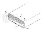
- FIG. 1 is a perspective view with a section taken along the width direction of the superconducting wire according to the first embodiment of the present invention.
- superconducting laminate 5 is formed by laminating intermediate layer 2, oxide superconducting layer 3, and metal stabilizing layer 4 in this order on one surface of substrate 1. That is, the intermediate layer 2 is formed on one surface of the substrate 1, the oxide superconducting layer 3 is formed on the outer side, and the metal stabilization layer 4 is formed on the outer side.
- the superconducting wire 10 is formed by the insulating coating layer 7 covering the entire outer surface of the superconducting laminate 5.
- the metal stabilization layer 4 includes a first stabilization layer 8 formed on the oxide superconducting layer 3 and a second stabilization layer 9 formed on the first stabilization layer 8.
- the outside refers to the side of each layer (element) opposite to the side where the substrate is provided, and the outer surface refers to the surface exposed to the outside of each layer (element).
- the substrate 11 only needs to be used as a substrate for a normal superconducting wire, and is preferably in the form of a long tape, and is preferably formed of a heat-resistant metal.
- heat-resistant metals nickel (Ni) alloys are more preferable.
- Hastelloy (trade name, manufactured by US Haynes Co., Ltd.) is suitable for commercial products, and has different amounts of components such as molybdenum (Mo), chromium (Cr), iron (Fe), and cobalt (Co). , C, G, N, and W can be used.
- an oriented metal substrate in which a texture is introduced into a nickel alloy or the like may be used as the substrate 1, and the intermediate layer 2 and the oxide superconducting layer 3 may be formed thereon.
- the thickness of the substrate 1 may be appropriately adjusted according to the purpose, and is usually preferably 10 to 500 ⁇ m, and more preferably 20 to 200 ⁇ m.
- the intermediate layer 2 controls the crystal orientation of the oxide superconducting layer 3 and prevents diffusion of metal elements in the substrate 1 toward the oxide superconducting layer 3 side. Further, the intermediate layer 2 functions as a buffer layer that alleviates the difference in physical properties (thermal expansion coefficient, lattice constant, etc.) between the substrate 1 and the oxide superconducting layer 3, and the material of the intermediate layer 2 is a physical property. Is preferably a metal oxide showing an intermediate value between the substrate 1 and the oxide superconducting layer 3.
- the constituent material of the intermediate layer 2 is Gd 2 Zr 2 O 7 , MgO, ZrO 2 —Y 2 O 3 (YSZ), SrTiO 3 , CeO 2 , Y 2 O 3 , Al 2 O 3 , Gd 2 Examples thereof include metal oxides such as O 3 , Zr 2 O 3 , Ho 2 O 3 , and Nd 2 O 3 .
- the intermediate layer 2 may be a single layer or a multilayer.
- the layer formed of the metal oxide (metal oxide layer) preferably has crystal orientation, and when it is a multilayer, it is the outermost layer (layer closest to the oxide superconducting layer 3). ) Preferably has at least crystal orientation.
- the intermediate layer 2 may have a multilayer structure in which a bed layer is interposed on the substrate 1 side.
- the bed layer has high heat resistance and is a layer for reducing interfacial reactivity, and is used for obtaining the orientation of a film disposed thereon.
- Such a bed layer is disposed as necessary, and is composed of, for example, yttria (Y 2 O 3 ), silicon nitride (Si 3 N 4 ), aluminum oxide (Al 2 O 3 , also referred to as “alumina”), or the like. Is done.
- the bed layer has a thickness of 10 to 200 nm, for example.
- the intermediate layer 2 may have a multilayer structure in which a diffusion preventing layer and a bed layer are laminated on the substrate 1 side.
- the intermediate layer 2 has a structure in which a diffusion preventing layer is interposed between the substrate 1 and the bed layer.
- the diffusion prevention layer is formed for the purpose of preventing the constituent elements of the substrate 1 from diffusing.
- the material of the diffusion prevention layer is composed of silicon nitride (Si 3 N 4 ), aluminum oxide (Al 2 O 3 ), rare earth metal oxide, or the like, and the thickness of the diffusion prevention layer is, for example, 10 to 400 nm.
- a combination using Al 2 O 3 as the diffusion preventing layer and Y 2 O 3 as the bed layer can be exemplified.
- the intermediate layer 2 may have a multilayer structure in which a cap layer is further laminated on the metal oxide layer.
- the cap layer has a function of controlling the orientation of the oxide superconducting layer 3, diffuses the elements constituting the oxide superconducting layer 3 into the intermediate layer 2, and gas used when the oxide superconducting layer 3 is laminated. And a function of suppressing the reaction between the intermediate layer 2 and the like.
- the cap layer is formed through a process of epitaxially growing on the surface of the metal oxide layer, and then growing the grains in the lateral direction (plane direction) (overgrowth) and selectively growing the crystal grains in the in-plane direction. It is preferred that Such a cap layer has a higher degree of in-plane orientation than the metal oxide layer.
- the material of the cap layer is not particularly limited as long as it is a material that can exhibit the above functions. Preferably, specifically, CeO 2, Y 2 O 3 , Al 2 O 3, Gd 2 O 3, Zr 2 O 3, Ho 2 O 3, Nd 2 O 3 and the like.
- the cap layer may include a Ce—M—O-based oxide in which part of Ce is substituted with another metal atom or metal ion.
- the thickness of the intermediate layer 12 may be appropriately adjusted according to the purpose, but is usually 0.1 to 5 ⁇ m.
- the intermediate layer 12 is formed by physical vapor deposition such as ion beam assisted vapor deposition (hereinafter abbreviated as IBAD); chemical vapor deposition (CVD); organometallic thermal decomposition (MOD); It can be laminated by a known method.
- IBAD ion beam assisted vapor deposition
- CVD chemical vapor deposition
- MOD organometallic thermal decomposition
- the metal oxide layer formed by the IBAD method is preferable in that the crystal orientation is high and the effect of controlling the crystal orientation of the oxide superconducting layer 3 and the cap layer is high.
- the oxide superconducting layer 3 As the material of the oxide superconducting layer 3, a material for forming an oxide superconductor having a generally known composition can be widely applied.
- REBa 2 Cu 3 O y RE is Y, La, Nd, Sm, Er, Examples thereof include Y123 (YBa 2 Cu 3 O y ) or Gd123 (GdBa 2 Cu 3 O y ).
- the oxide superconducting layer 13 is laminated by physical vapor deposition such as sputtering, vacuum vapor deposition, laser vapor deposition, or electron beam vapor deposition; chemical vapor deposition (CVD); coating pyrolysis (MOD). Of these, laser vapor deposition is preferred.
- the oxide superconducting layer 13 has a thickness of about 0.5 to 5 ⁇ m and preferably a uniform thickness.
- the first stabilization layer 8 laminated on the oxide superconducting layer 3 is formed of a metal material having good conductivity and low contact resistance with the oxide superconducting layer 3 such as Ag or a noble metal.
- the thickness is about 1 to 30 ⁇ m.
- the second stabilization layer 9 laminated on the first stabilization layer 8 is formed of a highly conductive metal material.
- the metal material constituting the second stabilization layer 9 is not particularly limited as long as it is a material having good conductivity.
- a copper alloy such as copper, brass (Cu—Zn alloy), Cu—Ni alloy, or the like
- a material formed of a relatively inexpensive material such as stainless steel.
- copper is preferable because it has high conductivity and is inexpensive.
- the second stabilizing layer 9 is formed of a resistance metal material, and a Ni-based alloy such as Ni—Cr can be used.
- the formation method of the 2nd stabilization layer 9 is not specifically limited, For example, by sticking the metal tape formed with highly conductive materials, such as copper, on the 1st stabilization layer 8 via joining materials, such as solder. Can be stacked.
- a metal tape may be provided without using a bonding material.
- a metal tape whose surface is covered with a bonding material may be used as the second stabilizing layer 9, a metal tape whose surface is covered with a bonding material may be used.
- the outer surface of the second stabilization layer 9, that is, the upper surface and both side surfaces of the second stabilization layer 9 shown in FIG. 1, has a maximum height (maximum height roughness) Rz (JIS B 0601: 2001). It is set to 890 nm or less.
- the maximum height of the outer surface of the second stabilization layer 9 is preferably 887 nm or less, and more preferably in the range of 189 to 887 nm.
- the surface roughness (arithmetic average roughness) Ra (JIS B 0601: 2001) of the outer surface of the second stabilization layer 9 is preferably 80 nm or less. Further, the surface roughness Ra of the outer surface of the second stabilizing layer 9 is more preferably in the range of 30 to 77 nm. In addition, it is more preferable that the outer surface of the second stabilizing layer 9 satisfies the range of the maximum height Rz described above and satisfies the range of the surface roughness Ra described above.
- the uneven state of the outer surface of the second stabilizing layer 9 affects the adhesion of the insulating coating layer 7.
- the unevenness of the outer surface of the second stabilization layer 9 is large, the anchor effect is generated by the large unevenness, and the adhesion of the insulating coating layer 7 is increased.
- the unevenness is small, the adhesion of the insulating coating layer 7 is reduced.
- the second stabilizing layer 9 and the insulating coating layer 7 There is a possibility that the intermediate layer 2 and a part of the superconducting layer 3 may be peeled off from the layer to which the intermediate layer 2 and the superconducting layer 3 are in close contact without being peeled off at the boundary portion.
- the intermediate layer 2 and the superconducting layer 3 do not peel from the layers to which the interlayer coating layer 7 and the insulating coating layer 7 are adhered, respectively, and the insulating coating layer 7 and the second stabilization It is preferable that the adhesive strength is such that it peels at the interface with the layer 9. For this reason, it is preferable to set the maximum height and surface roughness of the outer surface of the second stabilization layer 9 within the above-described ranges.
- solder that can be used when the second stabilization layer 9 is formed by laminating a metal tape on the first stabilization layer 8 via solder is not particularly limited, but a conventionally known solder can be used.
- solder formed of an alloy containing Sn as a main component, such as Sn—Ag alloy, Sn—Bi alloy, Sn—Cu alloy, or Sn—Zn alloy, Pb—Sn alloy Alloy solder, eutectic solder, low-temperature solder, and the like can be mentioned, and these solders can be used alone or in combination.
- the thickness of the second stabilizing layer 9 is not particularly limited and can be adjusted as appropriate, but is preferably 10 to 300 ⁇ m.
- a superconducting laminate 5 having a substantially rectangular cross section in which a substrate 1, an intermediate layer 2, an oxide superconducting layer 3, a first stabilizing layer 8, and a second stabilizing layer 9 are laminated has a cross section in the width direction.
- the four corners 5a are preferably curved surfaces having a radius of curvature. Since the corner portion 5a is a curved surface having a radius of curvature, the resin is uniformly applied and baked (cured) on the entire outer periphery including the corner portion 5a of the superconducting laminate 5 when the insulating coating layer 7 described later is formed. Insulating coating layer 7 that completely covers the entire outer periphery of superconducting laminate 5 can be formed.
- the superconducting laminate 5 can be completely sealed from the outside by the insulating coating layer 7.
- both corners on the bottom surface side of the substrate 1 are curved surfaces, and further, both corner portions on the upper surface side of the second stabilization layer 9 are curved surfaces.
- Four corners 5a are formed.
- the radius of curvature of the corner 5a is preferably set in the range of 15 ⁇ m to 150 ⁇ m.
- the corner portion of the superconducting laminate 5 is desired by polishing with a tool such as a scissors or a polishing apparatus. It can be processed to be the corner of the radius of curvature.
- the corner may be processed after the superconducting laminate 5 is formed.
- each layer may be laminated to form the superconducting laminate 5.
- the insulating coating layer 7 covering the entire outer periphery of the superconducting laminate 5 is formed by applying a resin to the entire outer periphery of the superconducting laminate 5 and then baking (curing), and the thickness thereof is set to 12 ⁇ m or more, for example. It is preferable that The upper limit of the thickness of the insulating coating layer 7 is not particularly limited, but is preferably 20 ⁇ m or less. By setting the thickness of the insulating coating layer 7 to 20 ⁇ m or less, the area of the insulating coating layer 7 occupying in the cross-sectional area of the superconducting wire 10 can be reduced. Therefore, the superconducting wire 10 can be reduced in size, and when the superconducting wire 10 is coiled, a necessary cross-sectional area of the superconducting layer 3 can be secured and a decrease in current density can be suppressed.
- the resin constituting the insulating coating layer 7 is not particularly limited as long as the layer can be formed by baking (curing).
- formal resin urethane resin, polyimide resin, polyamideimide resin, polyester resin, polyether ether ketone resin Fluorine resins such as (PEEK resin) and polytetrafluoroethylene (tetrafluorinated resin, PTFE).
- a resin that can be baked at a temperature of 200 ° C. or lower, for example, 170 to 200 ° C. is preferable.
- the baking temperature does not become too high, and the second stabilization layer 9 formed by bonding of a metal tape via solder or the like is used as the solder. It does not peel off due to melting.
- Baking of the resin when forming the insulating coating layer 7 is preferably performed at a temperature of 200 ° C. or less, for example, 170 to 200 ° C., and the baking time may be adjusted as appropriate. By baking the resin under such conditions, peeling of the second stabilization layer 9 due to melting of the solder and deterioration of the oxide superconducting layer 3 can be suppressed.
- the method for applying the resin is not particularly limited, and a conventionally known method such as a dip coating method or a spray coating method can be applied.
- the resin coating and baking process may be performed only once. The resin coating and baking process is performed until the insulating coating layer 7 having a desired thickness is formed. It may be repeated several times.
- the high temperature superconducting wire 10 of the present embodiment can realize a structure in which the entire outer periphery including the corner portion 5a of the superconducting laminate 5 is completely covered with the insulating coating layer 7. Therefore, in the high-temperature superconducting wire 10 of the present embodiment, the superconducting laminate 5 is sealed from the outside by the insulating coating layer 7, and it is possible to reduce the intrusion of moisture and the like into the oxide superconducting layer 3 and to deteriorate the superconducting characteristics. Can be suppressed. A part of the composition of the rare earth oxide superconductor reacts with moisture and thus is weak against moisture. Therefore, the influence of moisture can be eliminated by completely covering with the insulating coating layer 9.
- the oxide superconducting wire 10 when wound around a bobbin and coiled and fixed with an impregnating resin and cooled to a critical temperature or lower with a refrigerant, the oxide superconducting wire 10 and the second stabilizing substrate 1 having a large exclusive cross-sectional area Since the layer 9 is made of metal and the impregnating resin and the insulating coating layer 7 are made of resin, stress acts due to a difference in thermal expansion between the metal and the resin. Therefore, stress that causes delamination acts in the thickness direction of the oxide superconducting wire 10.
- the insulating coating layer 7 is in close contact with the second stabilizing layer 9 with an appropriate adhesive force, when a strong force acts in the direction causing delamination, the interface between the intermediate layer 2 and the superconducting layer 3 The stress is relieved by peeling the insulating coating layer 7 from the second stabilizing layer 9 before peeling occurs. For this reason, even if the oxide superconducting wire 10 of this embodiment is coiled and then fixed with an impregnation resin and cooled with a refrigerant, delamination between the intermediate layer 2 and the superconducting layer 3 does not occur, The oxide superconducting wire 10 and the superconducting coil in which the superconducting characteristics are not deteriorated can be obtained.
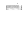
- FIG. 2 is a schematic cross-sectional view along the width direction of the superconducting wire according to the second embodiment of the present invention.
- the laminated base S2 is formed by laminating the intermediate layer 2, the oxide superconducting layer 3, and the first stabilizing layer 8 in this order on one surface of the substrate 1.
- the superconducting laminate 5B includes the laminated substrate S2 in the center, and the second stabilizing layer 12 is formed by covering the periphery (substantially the entire outer peripheral surface) of the laminated substrate S2, and has a substantially rectangular cross section. It is.
- the superconducting wire 10B is formed by covering the entire outer peripheral surface of the superconducting laminate 5B with the insulating coating layer 7B.
- the metal stabilization layer 4B is composed of a first stabilization layer 8 formed on the oxide superconducting layer 3 and a second stabilization layer 12 covering almost the entire circumference of the outer peripheral surface of the multilayer substrate S2. Has been.
- the second stabilization layer 12 of the present embodiment is formed of a highly conductive metal material, and when the oxide superconducting layer 3 transitions from the superconducting state to the normal conducting state, the oxide superconducting together with the first stabilizing layer 8. It functions as a bypass that commutates the current in layer 3.
- the second stabilization layer 12 in the form of a metal tape is arranged in a substantially C-shaped cross section along the peripheral surface of the multilayer substrate S2, and is provided so as to cover almost the entire peripheral surface of the multilayer substrate S2. More specifically, the second stabilization layer 12 is arranged so as to cover almost the entire circumference of the multilayer substrate S2 except for the central portion on the other surface (surface on which the intermediate layer 2 is not formed) side of the substrate 1. Yes.
- the superconducting wire of the first embodiment is that the second stabilizing layer 12 covers almost the entire circumference of the outer peripheral surface of the multilayer substrate S2 other than the portion where the solder layer 13 is provided. Different from the wire 10.
- the same components as those of the superconducting wire 10 shown in FIG. 1 are denoted by the same reference numerals, and detailed description thereof is omitted.
- Superconducting laminate 5B is a curved surface in which corner 12a of second stabilizing layer 12 in the cross section along the width direction has a radius of curvature. For this reason, when forming the insulating coating layer 7B, the resin can be applied and baked on the entire outer periphery including the corner portions 12a, and the insulating coating layer 7B covering the entire outer periphery of the second stabilizing layer 12 can be formed.
- the radius of curvature of the corner 12a is preferably set in the range of 15 ⁇ m to 150 ⁇ m.
- the insulating coating layer 7B is formed by applying a resin to the entire outer periphery of the second stabilizing layer 12 and then baking it.
- the resin constituting the insulating coating layer 7B is not particularly limited as long as the layer can be formed by baking, and the same resin material as that used in the superconducting wire 10 of the first embodiment can be used.
- the outer surface of the second stabilization layer 12 that is, the peripheral surface of the second stabilization layer 12 shown in FIG. 2, has a maximum height (maximum height roughness) Rz (JIS B0601: 2001) of 890 nm or less. Formed. Further, the maximum height Rz of the outer surface of the second stabilization layer 9 is preferably 887 nm or less, and more preferably in the range of 189 to 887 nm.
- the outer surface of the second stabilization layer 12 is preferably 80 nm or less in surface roughness (arithmetic average roughness) Ra. Furthermore, the surface roughness Ra of the outer surface of the second stabilization layer 12 is more preferably in the range of 30 to 77 nm.
- the maximum height of the outer surface of the second stabilizing layer 12 is defined within the above range and the above-described range of the surface roughness Ra is satisfied. In the present embodiment, it is not necessary that the entire outer surface of the second stabilization layer 12 is formed in the range of the above-described maximum height Rz and average roughness Ra. Since the second stabilization layer 12 of this embodiment is provided to prevent the intermediate layer 2 and part of the oxide superconducting layer 3 from being peeled off from the adhering layers, the intermediate layer 2 and the superconducting layer 3 are laminated. Only the outer surface of the second stabilization layer 12 positioned above the formed position may be formed to the aforementioned maximum height or average roughness.
- the superconducting wire 10B of the present embodiment can realize a structure in which the entire outer periphery including the corner 12a of the superconducting laminate 5B is completely covered with the insulating coating layer 7B. Therefore, in the high-temperature superconducting wire 10B of the present embodiment, the superconducting laminate 5B is sealed from the outside by the insulating coating layer 7B, so that moisture and the like can be prevented from entering the oxide superconducting layer 3, and the superconducting characteristics are deteriorated. Can be suppressed. If the corner portion 12a is not a curved surface, the resin around the corner portion may fall off or become thin when the resin is applied, and the insulating coating layer necessary to cover the corner portion may not be formed. Therefore, it is preferable that the corner portion 12a is a curved surface enough to allow the resin to sufficiently wrap around (formed on the corner portion 12a).
- the oxide superconducting wire 10B when the oxide superconducting wire 10B is wound around a bobbin and coiled and then fixed with an impregnating resin, and cooled to a critical temperature or lower with a refrigerant, stress acts due to the difference in thermal expansion between the metal and the resin, and the oxide There is a possibility that stress causing delamination may act along the thickness direction of the superconducting wire 10B.
- the insulating coating layer 7B peels off from the second stabilization layer 12 before the intermediate layer 2 and the superconducting layer 3 are peeled off from the layers to which the intermediate layer 2 and the superconducting layer 3 are in close contact. ease.
- the outer surface of the second stabilizing layer 12 is adjusted to an appropriate maximum height range or an appropriate surface roughness range, and the insulating coating layer 7B adheres to the second stabilizing layer 12 with an appropriate adhesion force. is doing. Therefore, the above-described stress can be relieved by peeling the insulating coating layer 7B from the second stabilizing layer 12 without causing peeling from the layer to which a part of the intermediate layer 2 and the superconducting layer 3 are adhered.
- the oxide superconducting wire 10B of the present embodiment is delaminated from the layer to which the intermediate layer 2 and the superconducting layer 3 are in close contact, even when the oxide superconducting wire 10B is coiled, fixed with an impregnating resin, and cooled with a refrigerant. do not do. Therefore, it is possible to obtain the oxide superconducting wire 10B and the superconducting coil that do not deteriorate the superconducting characteristics.
- FIG. 3 is a schematic cross-sectional view along the width direction of the high-temperature superconducting wire according to the third embodiment of the present invention.
- the laminated substrate S6 is formed by laminating the intermediate layer 2, the oxide superconducting layer 3, and the first stabilizing layer 8 on the substrate 1 in this order.
- the superconducting laminate 5F is formed by providing the laminated substrate S6 in the center and the entire outer periphery of the laminated substrate S6 is covered with the second stabilizing layer 22, and the superconducting laminate 5F has a substantially rectangular cross section. .
- an insulating coating layer 7F that covers the entire outer peripheral surface of the superconducting laminate 5F is formed on the outer peripheral surface of the superconducting laminate 5F via a bonding layer 23 formed of tin. Further, the bonding layer 23 may be formed on the entire outer peripheral surface of the superconducting laminate 5F.
- the entire outer periphery of the multilayer substrate S6 is covered with the second stabilization layer 22, but the present invention is not limited to this, and a part of the multilayer substrate S6 is covered as in the second embodiment. Alternatively, solder may be formed in part.
- solder layer may be provided between the laminated substrate S6 and the second stabilizing layer 22.
- the material for forming the bonding layer 23 is not limited to tin, and other solders can be used.
- the maximum height (maximum height roughness) Rz of the peripheral surface of the bonding layer 23 is set to 890 nm or less.
- the maximum height of the outer surface of the bonding layer 23 is preferably 887 nm or less, and more preferably in the range of 189 to 887 nm.
- the outer surface of the bonding layer 23 is preferably 80 nm or less in surface roughness Ra. Further, the surface roughness Ra of the outer surface of the bonding layer 23 is more preferably in the range of 30 to 77 nm.
- the outer surface of the bonding layer 23 satisfies the aforementioned range of the maximum height Rz and satisfies the aforementioned range of the surface roughness Ra.
- the corner portion 22a in the cross section along the width direction of the second stabilization layer 22 is a curved surface having a radius of curvature.
- the resin when forming the insulation coating layer 7F, the resin can be completely applied and baked on the entire outer periphery of the second stabilization layer 22 including the corner portions 22a, and the insulation covering the entire outer periphery of the superconducting laminate 5F.
- the coating layer 7F can be formed.
- the radius of curvature of the corner 22a is preferably set in the range of 15 ⁇ m to 150 ⁇ m.
- the same effects as the structures of the first and second embodiments described above can be obtained. That is, when a strong force acts in the direction causing delamination, the stress is relieved by peeling the insulating coating layer 7F from the outer surface of the bonding layer 23 before the intermediate layer 2 and the superconducting layer 3 are peeled off from the adhesive layers. To do. For this reason, the oxide superconducting wire 10F of the present embodiment is delaminated from the layer to which the intermediate layer 2 and the superconducting layer 3 are in close contact, even when the oxide superconducting wire 10F is coiled and fixed with an impregnating resin and cooled with a refrigerant. Thus, it is possible to obtain the oxide superconducting wire 10F and the superconducting coil in which the superconducting characteristics are not deteriorated.
- MgO metal oxide layer; film thickness: 10 nm
- IBAD method ion beam assisted sputtering
- PLD method pulse laser deposition
- a 0 ⁇ m-thick CeO 2 (cap layer) was formed.
- a 1.0 ⁇ m thick GdBa 2 Cu 3 O 7 oxide superconducting layer
- a 2 ⁇ m thick Ag layer is formed on the oxide superconducting layer by the sputtering method.
- a plurality of laminated bodies on which a fluorinated layer was formed were produced.
- a formal resin for example, Vinylec F, manufactured by Chisso Co., Ltd.
- a baking temperature of 185 ° C. on each of the produced superconducting laminates to form an insulating coating layer having a thickness of 20 ⁇ m.
- a plurality of superconducting wires were produced, and samples of Examples 1 and 2 were obtained.
- a superconducting laminate is formed by covering the laminate with a copper plating layer having a thickness of 20 ⁇ m instead of the 0.1 mm or 0.05 mm thick copper tape.
- the same formal resin insulating coating layer as in Examples 1 and 2 was formed, and a sample of Comparative Example 1 was obtained.
- Example 3 the base of the insulating coating layer described later is tin plating.
- Each superconducting wire sample produced was evaluated for superconducting properties and a peel test. For the measurement of superconducting properties, the critical current value at 77 K was measured for the superconducting laminate before baking the formal resin and the superconducting wire after baking, and the ratio of the critical current value before and after baking the formal resin was determined.
- the peel test was performed in accordance with the stud pull method using a cylindrical pin made of aluminum with a diameter of 2.7 mm. Adhesive was applied to the tip of this pin and pressed against the center of the top surface of the insulating coating layer. The tensile strength in the direction away from the insulating coating layer was taken as the peel strength.
- the resin coating layer is more easily peeled off from the Cu stabilization layer, so that the intermediate layer and the superconducting layer are protected and the insulating coating layer is peeled off from the Cu stabilization layer.
- the lower limit of the maximum height Rz is not particularly specified. Also, from the test results shown in Table 1, if the average roughness Ra of the surface of the copper stabilization layer that is the base of the resin coating layer is 80 nm or less, the intermediate layer and a part of the superconducting layer are peeled off from the layers that are in close contact with each other. It can be seen that no longer occurs.
- the number of turns of the coil was set to 200 turns (100 turns ⁇ 2), and the coil was wound around a GFRP winding frame to produce a superconducting coil.
- the parameters of the above superconducting coil are listed in Table 2 below.
- a superconducting wire in which an insulating coating layer is formed by wrapping two 12.5 ⁇ m-thick polyimide tapes over the structure of Example 3 instead of coating with formal resin is prepared. This was compared with the case where a superconducting coil was configured under the same conditions as the above-described superconducting coil using a wire. The above results are also shown in Table 2 below.
- the superconducting wire with an insulation coating layer formed by baking formal resin can improve the current density of the superconducting coil by 6% compared to the superconducting wire wrapped with polyimide tape. It turns out that. This difference is because the coil current density can be improved because the insulating layer can be made thinner in the coil of the embodiment even when the coil height, the inner and outer diameters of the coil, the number of turns, and the number of layers are almost the same.
- This superconducting wire was wound around the surface of a GFRP winding frame for about 31 turns, epoxy resin was supplied to the winding portion by vacuum impregnation, and the superconducting wire on the surface of the winding frame was fixed with the impregnating resin to obtain a superconducting coil example 1. .
- the critical current Ic of the superconducting wire in liquid nitrogen was measured. If two superconducting coils are manufactured and there is at least one superconducting coil whose critical current value has decreased by 10% or more before and after impregnation with epoxy resin, the evaluation is marked with x, and the critical current decreases for both of them. When it was not seen, the evaluation was marked with a circle.
- a width of 10 mm, a thickness of 0.19 mm (Hastelloy substrate thickness: 0.1 mm, Ag first stabilization layer thickness of 2 ⁇ m, stabilization copper plating layer thickness of 20 ⁇ m, coating layer thickness of 20 ⁇ m)
- the critical current Ic of the superconducting wire in liquid nitrogen was measured. If two superconducting coils are manufactured and there is at least one superconducting coil whose critical current value has decreased by 10% or more before and after impregnation with epoxy resin, the evaluation is marked with x, and the critical current decreases for both of them. When it was not seen, the evaluation was marked with a circle.
- the value of the maximum height Rz and the value of the surface roughness Ra are the same as those of the superconducting wire shown in Table 1. It is equivalent to the case.
- the sample of Example 1 did not show a decrease in critical current, and showed excellent results. Note that the superconducting wire constituting the superconducting coil of Conventional Example 1 has a width of 10 mm, and the superconducting wire constituting the superconducting coil of Example 1 has a width of 5 mm.
- the present invention provides a superconducting wire that can be used for a superconducting coil used in various superconducting devices such as a superconducting motor and a current limiting device.
Landscapes
- Chemical & Material Sciences (AREA)
- Engineering & Computer Science (AREA)
- Organic Chemistry (AREA)
- Power Engineering (AREA)
- Inorganic Chemistry (AREA)
- Ceramic Engineering (AREA)
- Superconductors And Manufacturing Methods Therefor (AREA)
- Inorganic Compounds Of Heavy Metals (AREA)
Abstract
Description
本願は、2012年2月29日に、日本に出願された特願2012-044554号に基づき優先権を主張し、その内容をここに援用する。
図5に示す超電導線材200は、テープ状の金属基材201上に中間層202を介して成膜法により酸化物超電導層203を積層し、その上にAg及びCuなどの安定化層204、205が積層される。そのため、図4に示すBi系の超電導線材100のように厚さ方向に対称的な構造の線材を用いて超電導コイルを設計する場合と異なり、希土類系の超電導線材200を用いて超電導コイルを形成するには、曲げ及び捻回などの方向性を考慮して設計する必要がある。
超電導線材を絶縁被覆する方法としては、テープ状の超電導線材の外周にポリイミドテープ等の樹脂テープを巻き付ける方法、及び超電導線材の外周面に樹脂を塗布して前記樹脂を焼付けることにより、超電導線材の外周面に樹脂被膜を形成する方法(特許文献1参照)が知られている。
また、樹脂を含浸させた超電導コイルでは、含浸材であるエポキシ樹脂と、超電導線材200を構成する金属製の基材201及びCu製の安定化層205との熱膨張差、あるいは、低温での熱膨張の非線形を考慮した収縮率に起因して、超電導コイルの冷却時に超電導線材200の垂直方向に剥離応力が作用し、超電導線材が劣化する可能性がある。
なお、エポキシ樹脂を含浸させる場合、真空含浸法を用いてコイルの隅々までエポキシ樹脂を浸透させる処理を行っている。一方、真空含浸法以外の方法で樹脂含浸を行うと、超電導コイルの機械的強度(コイル剛性)の低下を招くおそれがある。従って、真空含浸法が最も望ましいと考えられている。
例えば、金属基材201上に中間層202と酸化物超電導層203と安定化層204、205を積層した構造の場合、前述の剥離応力の作用によって、中間層202または超電導層203の一部の膜が剥がれるおそれがあった。
絶縁被覆層が密着される超電導積層体の外面の最大高さが890nm以下であれば、絶縁被覆層が超電導積層体外面に適度な密着力で付着する。従って、絶縁被覆層を含む超電導線材に応力が作用し、各層を剥離する方向に力が作用したとしても、絶縁被覆層と安定化層との界面で剥離が生じることで中間層と超電導層とでの剥離を抑制する。このため、超電導線材を超電導コイルに加工して含浸樹脂により固定し、冷媒で冷却し、金属と樹脂との熱膨張係数差に起因する熱応力を作用させたとしても、中間層及び超電導層で剥離を生じない超電導コイルを提供できる。
また、絶縁被覆層によって超電導積層体の全周を覆えば、外部からの水分の侵入を防止できる構造の超電導線材を提供できる。
絶縁被覆層が密着される超電導積層体の外面の表面粗さRaが80nm以下であれば、絶縁被覆層が超電導積層体の外面に適度な密着力で付着する。従って、絶縁被覆層を含む超電導線材に応力が作用し、各層を剥離する力が作用したとしても、絶縁被覆層と超電導積層体との界面で剥離が生じることで中間層及び超電導層がそれぞれ密着する層から剥離することを抑制する。
最大高さあるいは表面粗さを規定した超電導積層体の外面が超電導層の外方に積層される部分であることで、層間剥離を起こす方向に作用する応力を絶縁被覆層の超電導積層体からの剥離により緩和し、中間層及び超電導層がそれぞれ密着する層から剥離することを抑制する。
金属安定化層が第1安定化層と第2安定化層の2層構造である場合、上述の応力緩和性を具備した上に、超電導特性の安定性に優れた構造を提供できる。
超電導線材が、基板、中間層、超電導層、および第1安定化層の周囲を囲んで設けられた金属テープの第2安定化層を備えるならば、層間剥離を起こす方向に作用する応力を絶縁被覆層の超電導積層体からの剥離により緩和し、中間層及び超電導層がそれぞれ密着する層から剥離することを抑制する。また、金属テープの第2安定化層は、超電導層に流している電流を分流させる場合のバイパスとして作用する。
超電導線材が第1安定化層と第2安定化層に加えて第3安定化層を備えるならば、上述の応力緩和性を具備した上に、超電導層に流している電流を分流させる場合の金属安定化層の断面積をできるだけ確保することができる。従って、安定性向上に寄与する。
前記金属安定化層が、前記超電導層上に被覆された第1安定化層と、前記基板、前記中間層、前記超電導層、および前記第1安定化層の周囲を囲んで設けられる第2安定化層と、前記第2安定化層の外面に積層された接合層を有し、
前記接合層の外面が前記絶縁被覆層で覆われていてもよい。
超電導線材が第1安定化層と第2安定化層に加えて接合層を備え、接合層の外面の最大高さあるいは表面粗さを規定の範囲に揃えることで、層間剥離を起こす方向に作用する応力を絶縁被覆層の接合層からの剥離により緩和し、中間層及び超電導層がそれぞれ密着する層から剥離することを抑制することができる。
本発明の第2態様にかかる超電導コイルは、前述したいずれかの構造の超電導線材で形成される。
よって、本発明の態様に係る超電導線材をコイル化し、樹脂を含浸させて固定した場合であっても、超電導積層体の中間層の積層部分及び超電導層の積層部分において剥離することのない超電導線材を提供できる。
[第1実施形態]
図1は本発明の第1実施形態に係る超電導線材の幅方向に沿う一部を断面とした斜視図である。図1に示す超電導線材10において、超電導積層体5は、基板1の一面上に中間層2と酸化物超電導層3と金属安定化層4とがこの順に積層されることで形成される。つまり、基板1の一面上に中間層2が形成され、その外方に酸化物超電導層3が形成され、さらにその外方に金属安定化層4が形成される。さらに、超電導線材10は、絶縁被覆層7が超電導積層体5の外面全体を覆うことで形成される。本実施形態において金属安定化層4は、酸化物超電導層3上に形成された第1安定化層8と、第1安定化層8上に形成された第2安定化層9とにより構成される。ここで、本願において、外方とは、各層(要素)の、基板が設けられる側とは反対側をいい、外面とは、各層(要素)の外に露出した面をいう。
中間層2の構成材料として具体的には、Gd2Zr2O7、MgO、ZrO2-Y2O3(YSZ)、SrTiO3、CeO2、Y2O3、Al2O3、Gd2O3、Zr2O3、Ho2O3、Nd2O3等の金属酸化物を例示できる。
中間層2は、単層でも良いし、複層でも良い。例えば、前記金属酸化物で形成される層(金属酸化物層)は、結晶配向性を有していることが好ましく、複層である場合は、最外層(最も酸化物超電導層3に近い層)が少なくとも結晶配向性を有していることが好ましい。
さらに、中間層2は、基板1側に拡散防止層とベッド層が積層された複層構造でもよい。この場合、中間層2は、基板1とベッド層との間に拡散防止層が介在された構造を有する。拡散防止層は、基板1の構成元素拡散を防止する目的で形成される。拡散防止層の材料は、窒化ケイ素(Si3N4)、酸化アルミニウム(Al2O3)、あるいは希土類金属酸化物等で構成され、拡散防止層の厚さは例えば10~400nmである。基板1とベッド層との間に拡散防止層を介在させる場合の例としては、拡散防止層としてAl2O3、ベッド層としてY2O3を用いる組み合わせを例示することができる。
キャップ層の材質は、上記機能を発現し得る材質であれば特に限定されない。好ましくは、具体的には、CeO2、Y2O3、Al2O3、Gd2O3、Zr2O3、Ho2O3、Nd2O3等が例示できる。キャップ層の材質がCeO2である場合、キャップ層は、Ceの一部が他の金属原子又は金属イオンで置換されたCe-M-O系酸化物を含んでいても良い。
中間層12の厚さは、目的に応じて適宜調整すれば良いが、通常は、0.1~5μmである。
中間層12は、イオンビームアシスト蒸着法(以下、IBAD法と略記する)等の物理的蒸着法;化学気相成長法(CVD法);有機金属塗布熱分解法(MOD法);溶射等、公知の方法で積層できる。特に、IBAD法で形成された前記金属酸化物層は、結晶配向性が高く、酸化物超電導層3及びキャップ層の結晶配向性を制御する効果が高い点で好ましい。
酸化物超電導層13は、スパッタ法、真空蒸着法、レーザ蒸着法、電子ビーム蒸着法等の物理的蒸着法;化学気相成長法(CVD法);塗布熱分解法(MOD法)等で積層でき、中でもレーザ蒸着法が好ましい。
酸化物超電導層13の厚みは、0.5~5μm程度であって、均一な厚みであることが好ましい。
第2安定化層9を構成する金属材料としては、良導電性を有する材料であればよく、特に限定されないが、銅、黄銅(Cu-Zn合金)、Cu-Ni合金等の銅合金、またはステンレス等の比較的安価な材質で形成される材料を用いることが好ましく、中でも高い導電性を有し、安価であることから銅製が好ましい。
なお、酸化物超電導線材10を超電導限流器に使用する場合、第2安定化層9は抵抗金属材料で形成され、Ni-Cr等のNi系合金などを使用できる。
第2安定化層9の外面、即ち、図1に示す第2安定化層9の上面と両側面とは、それらの最大高さ(最大高さ粗さ)Rz(JIS B 0601:2001)を890nm以下としている。第2安定化層9の外面の最大高さは、887nm以下であることが好ましく、189~887nmの範囲であることがより好ましい。
また、第2安定化層9の外面の表面粗さ(算術平均粗さ)Ra(JIS B 0601:2001)は、80nm以下であることが好ましい。更に、第2安定化層9の外面の表面粗さRaについて、30~77nmの範囲であることがより好ましい。なお、第2安定化層9の外面が前述の最大高さRzの範囲を満たし、かつ、前述の表面粗さRaの範囲を満たすことがより好ましい。
第2安定化層9の厚さは特に限定されず、適宜調整可能であるが、10~300μmであることが好ましい。
超電導積層体5の角部5aを曲面に加工する場合、超電導積層体5を形成した後に角部を加工してもよい。また、予め基板1の両角部および第2安定化層9の両角部を曲面に加工した後に、各層を積層して超電導積層体5を形成してもよい。
絶縁被覆層7の厚さの上限は特に限定されないが、20μm以下とすることが好ましい。絶縁被覆層7の厚さを20μm以下とすることにより、超電導線材10の横断面積中に占める絶縁被覆層7の面積を削減できる。従って、超電導線材10を小型化できるとともに、超電導線材10をコイル加工した場合に、必要な超電導層3の断面積を確保して電流密度の低下を抑制できる。
これらの中でも、200℃以下、例えば、170~200℃の温度で焼付け可能な樹脂が好ましい。このような樹脂を用いることにより、絶縁被覆層7の形成時に、焼付け温度が高くなり過ぎることがなく、半田等を介した金属テープの貼り合わせにより形成されている第2安定化層9が半田の溶融により剥離することがない。
樹脂を塗布する方法は、特に限定されず、ディップコート法またはスプレーコート法等、従来公知の方法を適用することができる。
超電導積層体5に絶縁被覆層7を形成する方法は、樹脂の塗布・焼付け処理を一度だけ行ってもよく、所望の厚さの絶縁被覆層7が形成されるまで樹脂の塗布・焼付け処理を複数回繰り返し行ってもよい。
また、酸化物超電導線材10をボビンに巻き付けてコイル化した後に含浸樹脂で固定し、冷媒で臨界温度以下に冷却した場合、酸化物超電導線材10において専有断面積の大きな基板1と第2安定化層9とが金属製であり、含浸樹脂と絶縁被覆層7とが樹脂製であるので、金属と樹脂との熱膨張差に起因して応力が作用する。従って、酸化物超電導線材10の厚さ方向に層間剥離を起こす応力が作用する。この場合、絶縁被覆層7は第2安定化層9に対し適度な接着力で密着しているので、層間剥離を起こす方向に強い力が作用した場合、中間層2と超電導層3との界面で剥離が起こる前に絶縁被覆層7が第2安定化層9から剥離することで応力を緩和する。
このため、本実施形態の酸化物超電導線材10は、コイル化してから含浸樹脂で固定され、冷媒で冷却された場合であっても、中間層2と超電導層3との層間剥離が生じず、超電導特性の劣化しない酸化物超電導線材10および超電導コイルを得ることができる。
図2は本発明の第2実施形態に係る超電導線材の幅方向に沿う断面模式図である。
図2に示す超電導線材10Bにおいて、積層基体S2は、基板1の一方の面上に中間層2と酸化物超電導層3と第1安定化層8とがこの順に積層されることで形成され、矩形断面を有する。また、超電導積層体5Bは、上記積層基体S2を中央に備え、第2安定化層12が上記積層基体S2の周囲(外周面のほぼ全体)を覆うことで形成され、横断面が略矩形状である。さらに、超電導線材10Bは、絶縁被覆層7Bが前記超電導積層体5Bの外周面全体を覆うことで形成される。本実施形態において金属安定化層4Bは、酸化物超電導層3上に形成された第1安定化層8と、積層基体S2の外周面のほぼ全周を覆う第2安定化層12とで構成されている。
第2安定化層12を構成する金属材料は、先に説明した第1実施形態の第2安定化層9を構成する金属材料を適用でき、その厚さについても同等の範囲を選択できる。なお、図2では略されているが、金属テープ状の第2安定化層12を積層基体S2の外周に半田を介して一体化する場合は、積層基体S2と第2安定化層12との間には半田層が存在する。
図2に示す超電導線材10Bにおいて図1に示す超電導線材10と同一の構成要素には同一の符号を付し、詳細な説明を略する。
絶縁被覆層7Bは、第2安定化層12の外周全体に樹脂を塗布した後、焼付けすることにより形成されている。絶縁被覆層7Bを構成する樹脂としては、焼付けにより層を形成できれば特に限定されず、前記第1実施形態の超電導線材10で用いた樹脂と同様の樹脂材料が挙げられる。
前記第2安定化層12の外面は、表面粗さ(算術平均粗さ)Raにおいて80nm以下であることが好ましい。更に、第2安定化層12の外面の表面粗さRaについて、30~77nmの範囲であることがより好ましい。更に、第2安定化層12の外面の最大高さを前記範囲に規定した上に前述の表面粗さRaの範囲を満たすことがより好ましい。なお、本実施形態において、第2安定化層12の外面の全部が上述の最大高さRzと平均粗さRaの値の範囲で形成されている必要はない。本実施形態の第2安定化層12は中間層2及び酸化物超電導層3の一部がそれぞれ密着する層から剥離することを防止するために設けられるので、中間層2と超電導層3が積層された位置の上方に位置する第2安定化層12の外面のみを前述の最大高さまたは平均粗さに形成すればよい。
このため、本実施形態の酸化物超電導線材10Bは、コイル化してから含浸樹脂で固定され、冷媒で冷却された場合であっても、中間層2及び超電導層3がそれぞれ密着する層から層間剥離しない。したがって、超電導特性の劣化しない酸化物超電導線材10Bおよび超電導コイルを得ることができる。
図3は本発明の第3実施形態に係る高温超電導線材の幅方向に沿う断面模式図である。
図3に示す高温超電導線材10Fにおいて、積層基体S6は、基板1上に中間層2と酸化物超電導層3と第1安定化層8とがこの順に積層されることで形成される。さらに超電導積層体5Fは、積層基体S6を中央に備え、この積層基体S6の外周全体が第2安定化層22により覆われることで形成され、超電導積層体5Fの横断面は略矩形状である。さらに、超電導積層体5Fの外周面上に、スズで形成される接合層23を介して超電導積層体5Fの外周面全体を覆う絶縁被覆層7Fが形成されている。また、接合層23は超電導積層体5Fの全外周面上に形成されていてもよい。なお、図3では、積層基体S6の外周全体が第2安定化層22により覆われているが、本発明はそれに限られず、第2実施形態のように積層基体S6の一部が覆われておらず、一部に半田が形成されていてもよい。第2実施形態と同様に、半田を用いて積層基体S6と第2安定化層22とを一体化する場合、積層基体S6と第2安定化層22との間に半田層を設けてもよい。また、接合層23を形成する材料はスズに限られず、その他の半田を用いることができる。図3に示す超電導線材10Fにおいて図1に示す超電導線材10と同一の構成要素には同一の符号を付し、詳細な説明を省略する。
また、接合層23の外面の最大高さは、887nm以下であることが好ましく、189~887nmの範囲であることがより好ましい。
前記接合層23の外面は、表面粗さRaにおいて80nm以下であることが好ましい。
更に、接合層23の外面の表面粗さRaについて、30~77nmの範囲であることがより好ましい。更に、接合層23の外面が前述の最大高さRzの範囲を満たし、かつ、前述の表面粗さRaの範囲を満たすことがより好ましい。
なお、本実施形態において、接合層23の外面の全部が上述の最大高さ及び平均粗さに形成されている必要はない。本実施形態は中間層2及び酸化物超電導層がそれぞれ密着する層から剥離することを防止すればよいので、中間層2と超電導層3が積層された位置の上方に位置する接合層23の外面のみを前述の最大高さまたは平均粗さに形成してもよい。
即ち、層間剥離を起こす方向に強い力が作用した場合、中間層2及び超電導層3がそれぞれ密着する層から剥離する前に絶縁被覆層7Fが接合層23の外面から剥離することで応力を緩和する。
このため、本実施形態の酸化物超電導線材10Fは、コイル化してから含浸樹脂で固定され、冷媒で冷却された場合であっても、中間層2及び超電導層3がそれぞれ密着する層から層間剥離せず、超電導特性の劣化しない酸化物超電導線材10Fおよび超電導コイルを得ることができる。
幅5mm、厚さ0.1mmのテープ状のハステロイ(米国ヘインズ社製商品名)製の基板上に、スパッタ法によりAl2O3(拡散防止層;膜厚150nm)を成膜した上に、イオンビームスパッタ法によりY2O3(ベッド層;膜厚20nm)を成膜した。次いで、このベッド層上に、イオンビームアシストスパッタ法(IBAD法)によりMgO(金属酸化物層;膜厚10nm)を形成し、このMgO層上に、パルスレーザー蒸着法(PLD法)により1.0μm厚のCeO2(キャップ層)を成膜した。次いで、CeO2層上にPLD法により1.0μm厚のGdBa2Cu3O7(酸化物超電導層)を形成し、さらに酸化物超電導層上にスパッタ法により2μm厚のAg層(第1安定化層)を形成した積層体を複数作製した。
その後、これらの積層体に0.1mm厚のCuテープ(第2安定化層)あるいは0.05mm厚のCuテープを、スズ半田(融点230℃)によりAg層上に貼り合わせ、幅5mm、厚さ0.19mmあるいは厚さ0.14mmの超電導積層体を作製した。
また、前述の実施例において、0.1mm厚あるいは0.05mm厚の銅テープに代え、積層体に厚さ20μmの銅めっき層を被覆して超電導積層体を構成し、この超電導積層体に実施例1及び2と同じホルマール樹脂の絶縁被覆層を形成し、比較例1の試料を得た。
次に、前述の実施例において、0.1mm厚あるいは0.05mm厚の銅テープに代え、表面にスズめっきを施した銅テープをロールを用いたフォーミングを超電導積層体の周囲に被覆した構造の超電導線材を作製し、実施例3の試料を得た。なお、実施例3において、後述する絶縁被覆層の下地は、スズめっきとなる。
作製した各超電導線材試料について、超電導特性、剥離試験の評価を行った。
超電導特性の測定は、ホルマール樹脂の焼付け前の超電導積層体と焼付け後の超電導線材について77Kにおける臨界電流値を測定し、ホルマール樹脂焼付け前と焼付け後の臨界電流値の比を求めた。
剥離試験は、スタッドプル法に従い、φ2.7mmのアルミニウム製の円柱状のピンを用い、このピンの先端に接着剤を付けて絶縁被覆層の上面中央部に押しつけ、加熱硬化後にピンを軸方向に絶縁被覆層から離れる方向に引張り、その際の破壊強度を剥離強度とした。

これに対し、最大高さRzの値が比較例1の試料よりも小さい実施例1~3の試料は、いずれも絶縁被覆層が安定化層から剥離したが、中間層と超電導層とがそれぞれ密着する部分で剥離を生じることは無かった。絶縁被覆層は絶縁のために形成されている。従って、多少剥離を生じたとしても絶縁被覆層がCuの安定化層の上に存在していれば絶縁効果は得られるので使用に支障はない。これに対し、中間層あるいは超電導層の部分で剥離が生じると、超電導層を部分的に損傷するため、超電導特性に悪影響を及ぼす。
また、表1に示す試験結果から、樹脂被覆層の下地となる銅安定化層表面の平均粗さRaが、80nm以下であれば、中間層及び超電導層の一部がそれぞれ密着する層から剥離を生じなくなることが分かる。また、表1に示す結果から77nm以下であれば、中間層及び超電導層の一部がそれぞれ密着する層から剥離を生じなくなくなる。また、実施例1~3の結果からみて平均粗さRaを30~77nmの範囲にすれば、中間層及び超電導層の一部がそれぞれ密着する層から剥離を生じない。
なお、比較例1では第2安定化層に銅めっき層を用いる例を示しているが、銅めっき層の最大高さRz及び平均粗さRaが上記範囲であれば、本発明に銅めっき層を用いることは除外されず、上記範囲を満たす銅めっき層を用いてもよい。
線材幅10mm、0.19mm厚(0.1mm厚のハステロイ基板+Agの安定化層厚2μm+銅の安定化層の厚さ20μm、絶縁被覆層による被覆厚20μm)とした超電導線材を用い、超電導コイルとしてコイル内径70mm、高さ20.5mmのダブルパンケーキ型コイルを作製した。なお、基板上に形成した拡散防止層とベッド層と金属酸化物層とキャップ層と酸化物超電導層とは先の実施例3の各層と同等である。
コイルのターン数を200ターン(100ターン×2)としてGFRP製の巻き枠に巻き付け、超電導コイルを作製した。
以上の超電導コイルの各パラメータを以下の表2に記載する。
また、実施例3の構造に対し、従来例として、ホルマール樹脂で被覆する代わりに厚さ12.5μmのポリイミドテープを2枚重ね巻きして絶縁被覆層を形成した超電導線材を用意し、この超電導線材を用いて上述の超電導コイルと同等条件で超電導コイルを構成した場合と対比した。
以上の結果を以下の表2に併せて記載する。

この差は、ほぼ同じコイル高さ、コイル内外径、ターン数、層数であっても、実施例のコイルの方が絶縁層を薄くできるためにコイル電流密度を向上できたためである。
幅5mm、厚さ0.19mm(ハステロイ基板厚:0.1mm、Agの第1安定化層厚2μm、安定化銅層厚20μm、被覆層厚20μm)の超電導線材(線材臨界電流Ic=205~221A(77K、自己磁場中))を用意した。この超電導線材をGFRP製の巻枠の表面に約31ターン巻き付け、エポキシ樹脂を真空含浸により巻き付け部に供給し、巻き枠表面の超電導線材を含浸樹脂により固定し、超電導コイル実施例1を得た。
エポキシ樹脂を真空含浸する前と後において、それぞれ液体窒素中における超電導線材の臨界電流Icを測定した。超電導コイルは2個作製し、エポキシ樹脂の含浸前後で10%以上、臨界電流値が低下している超電導コイルが1個でもある場合は、評価を×印とし、2個とも臨界電流の低下が見られなかった場合は評価を○印とした。
また、比較のために、従来例として、幅10mm、厚さ0.19mm(ハステロイ基板厚:0.1mm、Agの第1安定化層厚2μm、安定化銅めっき層厚20μm、被覆層厚20μm)の超電導線材(線材臨界電流Ic=492~520A(77K、自己磁場中))を用意した。
この超電導線材をGFRP製の巻枠の表面に約31ターン巻き付け、エポキシ樹脂を真空含浸により巻き付け部に供給し、巻き枠表面の超電導線材を含浸樹脂により固定し、超電導コイル従来例1を得た。
エポキシ樹脂を真空含浸する前と後において、それぞれ液体窒素中における超電導線材の臨界電流Icを測定した。超電導コイルは2個作製し、エポキシ樹脂の含浸前後で10%以上、臨界電流値が低下している超電導コイルが1個でもある場合は、評価を×印とし、2個とも臨界電流の低下が見られなかった場合は評価を○印とした。

表3に示すように実施例1の試料は臨界電流の低下が見られず、優れた結果を示した。
なお、従来例1の超電導コイルを構成した超電導線材は幅10mm、実施例1の超電導コイルを構成した超電導線材は幅5mmであるので、両者の線材Ic値は異なっている。
Claims (7)
- 超電導線材であって、
基板と、前記基板に積層された中間層と超電導層と金属安定化層とを有する超電導積層体と、
前記超電導積層体の外面を覆い、樹脂材料を焼付けることにより形成された絶縁被覆層と、を備え、
前記絶縁被覆層に覆われた前記超電導積層体の外面の少なくとも一部の最大高さRzが890nm以下であることを特徴とする超電導線材。 - 請求項1に記載の超電導線材であって、
前記絶縁被覆層に覆われた前記超電導積層体の外面の少なくとも一部の表面粗さRaが80nm以下であることを特徴とする超電導線材。 - 請求項1または請求項2に記載の超電導線材であって、
前記超電導積層体の外面の少なくとも一部は前記超電導層の外方に積層される層の外面を含むことを特徴とする超電導線材。 - 請求項1~3のいずれか一項に記載の超電導線材であって、
前記金属安定化層が、第1安定化層と、前記第1安定化層上に積層された第2安定化層を有し、
前記第2安定化層が金属テープまたは前記金属テープと接合材とで形成され、前記金属テープの外面または前記接合材の外面が前記絶縁被覆層で覆われることを特徴とする超電導線材。 - 請求項1~3のいずれか一項に記載の超電導線材であって、
前記金属安定化層が、前記超電導層上に被覆された第1安定化層と、前記基板、前記中間層、前記超電導層、および前記第1安定化層の周囲を囲んで設けられ、金属テープで形成される第2安定化層と、を有し、前記第2安定化層の外面が前記絶縁被覆層で覆われていることを特徴とする超電導線材。 - 請求項1~3のいずれか一項に記載の超電導線材であって、
前記金属安定化層が、前記超電導層上に被覆された第1安定化層と、前記基板、前記中間層、前記超電導層、および前記第1安定化層の周囲を囲んで設けられる第2安定化層と、前記第2安定化層の外面に積層された接合層を有し、
前記接合層の外面が前記絶縁被覆層で覆われることを特徴とする超電導線材。 - 請求項1~6のいずれか一項に記載の超電導線材で形成されることを特徴とする超電導コイル。
Priority Applications (3)
| Application Number | Priority Date | Filing Date | Title |
|---|---|---|---|
| EP13755650.2A EP2801983B1 (en) | 2012-02-29 | 2013-02-28 | Superconducting wire and superconducting coil |
| JP2014502365A JP5693784B2 (ja) | 2012-02-29 | 2013-02-28 | 超電導線材および超電導コイル |
| US14/459,473 US9564259B2 (en) | 2012-02-29 | 2014-08-14 | Superconducting wire and superconducting coil |
Applications Claiming Priority (2)
| Application Number | Priority Date | Filing Date | Title |
|---|---|---|---|
| JP2012044554 | 2012-02-29 | ||
| JP2012-044554 | 2012-02-29 |
Related Child Applications (1)
| Application Number | Title | Priority Date | Filing Date |
|---|---|---|---|
| US14/459,473 Continuation US9564259B2 (en) | 2012-02-29 | 2014-08-14 | Superconducting wire and superconducting coil |
Publications (1)
| Publication Number | Publication Date |
|---|---|
| WO2013129568A1 true WO2013129568A1 (ja) | 2013-09-06 |
Family
ID=49082759
Family Applications (1)
| Application Number | Title | Priority Date | Filing Date |
|---|---|---|---|
| PCT/JP2013/055391 Ceased WO2013129568A1 (ja) | 2012-02-29 | 2013-02-28 | 超電導線材および超電導コイル |
Country Status (4)
| Country | Link |
|---|---|
| US (1) | US9564259B2 (ja) |
| EP (1) | EP2801983B1 (ja) |
| JP (1) | JP5693784B2 (ja) |
| WO (1) | WO2013129568A1 (ja) |
Cited By (16)
| Publication number | Priority date | Publication date | Assignee | Title |
|---|---|---|---|---|
| WO2014129586A1 (ja) * | 2013-02-25 | 2014-08-28 | 株式会社フジクラ | 高温超電導コイルおよび超電導機器 |
| WO2015098934A1 (ja) * | 2013-12-25 | 2015-07-02 | 株式会社フジクラ | 酸化物超電導線材及び酸化物超電導線材の製造方法 |
| JP2015198017A (ja) * | 2014-04-01 | 2015-11-09 | 住友電気工業株式会社 | 酸化物超電導薄膜線材 |
| JP2015198015A (ja) * | 2014-04-01 | 2015-11-09 | 住友電気工業株式会社 | 酸化物超電導薄膜線材 |
| WO2016017204A1 (ja) * | 2014-07-31 | 2016-02-04 | 住友電気工業株式会社 | 超電導線材 |
| KR20170028837A (ko) * | 2015-09-04 | 2017-03-14 | 한국전기연구원 | 스마트 인슐레이션을 구비하는 고온 초전도 코일, 그에 사용되는 고온 초전도 선재 및 그 제조방법 |
| EP3046116A4 (en) * | 2013-09-11 | 2017-04-26 | Sunam Co. Ltd. | Superconductor and method of manufacturing same |
| CN107077927A (zh) * | 2014-08-05 | 2017-08-18 | 株式会社藤仓 | 氧化物超导线材、超导设备及氧化物超导线材的制造方法 |
| JP2018206521A (ja) * | 2017-05-31 | 2018-12-27 | 株式会社フジクラ | 高温超電導線材及び超電導コイル |
| JP2018206670A (ja) * | 2017-06-07 | 2018-12-27 | 株式会社フジクラ | 酸化物超電導線材、超電導コイル、および酸化物超電導線材の製造方法 |
| KR20190071732A (ko) * | 2016-10-31 | 2019-06-24 | 스미토모 덴키 고교 가부시키가이샤 | 초전도 선재 및 초전도 코일 |
| JPWO2021100789A1 (ja) * | 2019-11-18 | 2021-05-27 | ||
| JP2022108794A (ja) * | 2021-01-14 | 2022-07-27 | 住友重機械工業株式会社 | 超電導コイル装置 |
| US11710583B2 (en) | 2020-04-06 | 2023-07-25 | Fujikura Ltd. | Oxide superconducting wire and superconducting coil |
| JPWO2023176193A1 (ja) * | 2022-03-14 | 2023-09-21 | ||
| WO2023176194A1 (ja) * | 2022-03-14 | 2023-09-21 | 住友電気工業株式会社 | 超電導線材および超電導機器 |
Families Citing this family (6)
| Publication number | Priority date | Publication date | Assignee | Title |
|---|---|---|---|---|
| ITPD20130284A1 (it) * | 2013-10-16 | 2015-04-17 | Columbus Superconductors S P A | Impianto di brasatura in continuo e processo di brasatura |
| WO2018078877A1 (ja) * | 2016-10-31 | 2018-05-03 | 住友電気工業株式会社 | 超電導線材 |
| DE102017221129A1 (de) * | 2017-11-27 | 2019-05-29 | Siemens Aktiengesellschaft | Supraleitender Bandleiter mit flächiger Schutzschicht |
| US11482342B2 (en) | 2018-10-07 | 2022-10-25 | Tanner L. Horne | Nuclear fusion reactor with toroidal superconducting magnetic coils implementing inertial electrostatic heating |
| DE102018217480A1 (de) * | 2018-10-12 | 2020-04-16 | Siemens Aktiengesellschaft | Supraleitender Bandleiter mit flächiger Isolationsschicht |
| JP6743233B1 (ja) * | 2019-03-28 | 2020-08-19 | 株式会社フジクラ | 酸化物超電導線材 |
Citations (10)
| Publication number | Priority date | Publication date | Assignee | Title |
|---|---|---|---|---|
| JP2000311526A (ja) | 1999-02-26 | 2000-11-07 | Sumitomo Electric Ind Ltd | 絶縁被膜を有する酸化物超電導線材およびその製造方法 |
| JP2008243588A (ja) * | 2007-03-27 | 2008-10-09 | Toshiba Corp | 高温超電導線材、高温超電導コイルおよびその製造方法 |
| JP2008244249A (ja) * | 2007-03-28 | 2008-10-09 | Toshiba Corp | 高温超電導コイル |
| JP2010176892A (ja) * | 2009-01-27 | 2010-08-12 | Sumitomo Electric Ind Ltd | 超電導線材および超電導線材の製造方法 |
| JP2010267822A (ja) * | 2009-05-14 | 2010-11-25 | Toshiba Corp | 超電導コイル装置 |
| JP2010267550A (ja) * | 2009-05-15 | 2010-11-25 | Toshiba Corp | 離形材付き高温超電導線材および超電導コイル |
| JP2011008949A (ja) * | 2009-06-23 | 2011-01-13 | Fujikura Ltd | 超電導線材及びその製造方法 |
| JP2011138706A (ja) * | 2009-12-28 | 2011-07-14 | Fujikura Ltd | 超電導線材の修復方法及び修復構造を有する超電導線材 |
| JP2012033947A (ja) * | 2011-09-27 | 2012-02-16 | Toshiba Corp | 高温超電導コイルおよびその製造方法 |
| JP2012216504A (ja) * | 2011-03-31 | 2012-11-08 | Fujikura Ltd | 高温超電導線材および高温超電導コイル |
Family Cites Families (7)
| Publication number | Priority date | Publication date | Assignee | Title |
|---|---|---|---|---|
| JPH07169343A (ja) | 1993-10-21 | 1995-07-04 | Sumitomo Electric Ind Ltd | 超電導ケーブル導体 |
| US6925316B2 (en) * | 2002-04-08 | 2005-08-02 | Christopher M. Rey | Method of forming superconducting magnets using stacked LTS/HTS coated conductor |
| US20040266628A1 (en) * | 2003-06-27 | 2004-12-30 | Superpower, Inc. | Novel superconducting articles, and methods for forming and using same |
| JP4300517B2 (ja) | 2003-09-24 | 2009-07-22 | 住友電気工業株式会社 | 超電導ケーブル |
| JP5119582B2 (ja) * | 2005-09-16 | 2013-01-16 | 住友電気工業株式会社 | 超電導線材の製造方法および超電導機器 |
| KR20090003826A (ko) * | 2007-07-04 | 2009-01-12 | 주식회사 코오롱 | 폴리이미드 필름 |
| KR101822118B1 (ko) * | 2010-07-06 | 2018-01-25 | 아토테크 도이칠란드 게엠베하 | 금속 표면의 처리 방법 및 그에 의해 형성된 장치 |
-
2013
- 2013-02-28 EP EP13755650.2A patent/EP2801983B1/en active Active
- 2013-02-28 WO PCT/JP2013/055391 patent/WO2013129568A1/ja not_active Ceased
- 2013-02-28 JP JP2014502365A patent/JP5693784B2/ja active Active
-
2014
- 2014-08-14 US US14/459,473 patent/US9564259B2/en active Active
Patent Citations (10)
| Publication number | Priority date | Publication date | Assignee | Title |
|---|---|---|---|---|
| JP2000311526A (ja) | 1999-02-26 | 2000-11-07 | Sumitomo Electric Ind Ltd | 絶縁被膜を有する酸化物超電導線材およびその製造方法 |
| JP2008243588A (ja) * | 2007-03-27 | 2008-10-09 | Toshiba Corp | 高温超電導線材、高温超電導コイルおよびその製造方法 |
| JP2008244249A (ja) * | 2007-03-28 | 2008-10-09 | Toshiba Corp | 高温超電導コイル |
| JP2010176892A (ja) * | 2009-01-27 | 2010-08-12 | Sumitomo Electric Ind Ltd | 超電導線材および超電導線材の製造方法 |
| JP2010267822A (ja) * | 2009-05-14 | 2010-11-25 | Toshiba Corp | 超電導コイル装置 |
| JP2010267550A (ja) * | 2009-05-15 | 2010-11-25 | Toshiba Corp | 離形材付き高温超電導線材および超電導コイル |
| JP2011008949A (ja) * | 2009-06-23 | 2011-01-13 | Fujikura Ltd | 超電導線材及びその製造方法 |
| JP2011138706A (ja) * | 2009-12-28 | 2011-07-14 | Fujikura Ltd | 超電導線材の修復方法及び修復構造を有する超電導線材 |
| JP2012216504A (ja) * | 2011-03-31 | 2012-11-08 | Fujikura Ltd | 高温超電導線材および高温超電導コイル |
| JP2012033947A (ja) * | 2011-09-27 | 2012-02-16 | Toshiba Corp | 高温超電導コイルおよびその製造方法 |
Non-Patent Citations (1)
| Title |
|---|
| See also references of EP2801983A4 |
Cited By (28)
| Publication number | Priority date | Publication date | Assignee | Title |
|---|---|---|---|---|
| US10049800B2 (en) | 2013-02-25 | 2018-08-14 | Fujikura Ltd. | High-temperature superconducting coil and superconducting device |
| WO2014129586A1 (ja) * | 2013-02-25 | 2014-08-28 | 株式会社フジクラ | 高温超電導コイルおよび超電導機器 |
| US10262776B2 (en) | 2013-09-11 | 2019-04-16 | Sunam Co., Ltd. | Superconductor and method of manufacturing same |
| EP3046116A4 (en) * | 2013-09-11 | 2017-04-26 | Sunam Co. Ltd. | Superconductor and method of manufacturing same |
| WO2015098934A1 (ja) * | 2013-12-25 | 2015-07-02 | 株式会社フジクラ | 酸化物超電導線材及び酸化物超電導線材の製造方法 |
| JPWO2015098934A1 (ja) * | 2013-12-25 | 2017-03-23 | 株式会社フジクラ | 酸化物超電導線材及び酸化物超電導線材の製造方法 |
| EP3089172A4 (en) * | 2013-12-25 | 2017-08-30 | Fujikura Ltd. | Oxide superconducting wire material and oxide superconducting wire material manufacturing method |
| JP2015198017A (ja) * | 2014-04-01 | 2015-11-09 | 住友電気工業株式会社 | 酸化物超電導薄膜線材 |
| JP2015198015A (ja) * | 2014-04-01 | 2015-11-09 | 住友電気工業株式会社 | 酸化物超電導薄膜線材 |
| WO2016017204A1 (ja) * | 2014-07-31 | 2016-02-04 | 住友電気工業株式会社 | 超電導線材 |
| CN107077927A (zh) * | 2014-08-05 | 2017-08-18 | 株式会社藤仓 | 氧化物超导线材、超导设备及氧化物超导线材的制造方法 |
| EP3179486A4 (en) * | 2014-08-05 | 2018-04-11 | Fujikura Ltd. | Oxide superconducting wire, superconducting device and method for producing oxide superconducting wire |
| US10128025B2 (en) | 2014-08-05 | 2018-11-13 | Fujikura Ltd. | Oxide superconducting wire, superconducting device, and method for producing oxide superconducting wire |
| CN107077927B (zh) * | 2014-08-05 | 2019-09-24 | 株式会社藤仓 | 氧化物超导线材、超导设备及氧化物超导线材的制造方法 |
| KR102494710B1 (ko) * | 2015-09-04 | 2023-02-02 | 한국전기연구원 | 스마트 인슐레이션을 구비하는 고온 초전도 코일, 그에 사용되는 고온 초전도 선재 및 그 제조방법 |
| KR20170028837A (ko) * | 2015-09-04 | 2017-03-14 | 한국전기연구원 | 스마트 인슐레이션을 구비하는 고온 초전도 코일, 그에 사용되는 고온 초전도 선재 및 그 제조방법 |
| KR20190071732A (ko) * | 2016-10-31 | 2019-06-24 | 스미토모 덴키 고교 가부시키가이샤 | 초전도 선재 및 초전도 코일 |
| KR102562414B1 (ko) * | 2016-10-31 | 2023-08-01 | 스미토모 덴키 고교 가부시키가이샤 | 초전도 선재 및 초전도 코일 |
| JP2018206521A (ja) * | 2017-05-31 | 2018-12-27 | 株式会社フジクラ | 高温超電導線材及び超電導コイル |
| JP2018206670A (ja) * | 2017-06-07 | 2018-12-27 | 株式会社フジクラ | 酸化物超電導線材、超電導コイル、および酸化物超電導線材の製造方法 |
| JPWO2021100789A1 (ja) * | 2019-11-18 | 2021-05-27 | ||
| US11710583B2 (en) | 2020-04-06 | 2023-07-25 | Fujikura Ltd. | Oxide superconducting wire and superconducting coil |
| JP2022108794A (ja) * | 2021-01-14 | 2022-07-27 | 住友重機械工業株式会社 | 超電導コイル装置 |
| JP7544606B2 (ja) | 2021-01-14 | 2024-09-03 | 住友重機械工業株式会社 | 超電導コイル装置 |
| JPWO2023176193A1 (ja) * | 2022-03-14 | 2023-09-21 | ||
| WO2023176193A1 (ja) * | 2022-03-14 | 2023-09-21 | 住友電気工業株式会社 | 超電導線材および超電導機器 |
| WO2023176194A1 (ja) * | 2022-03-14 | 2023-09-21 | 住友電気工業株式会社 | 超電導線材および超電導機器 |
| JPWO2023176194A1 (ja) * | 2022-03-14 | 2023-09-21 |
Also Published As
| Publication number | Publication date |
|---|---|
| US20140357495A1 (en) | 2014-12-04 |
| EP2801983A4 (en) | 2015-09-02 |
| US9564259B2 (en) | 2017-02-07 |
| EP2801983A1 (en) | 2014-11-12 |
| EP2801983B1 (en) | 2017-07-19 |
| JPWO2013129568A1 (ja) | 2015-07-30 |
| JP5693784B2 (ja) | 2015-04-01 |
Similar Documents
| Publication | Publication Date | Title |
|---|---|---|
| JP5693784B2 (ja) | 超電導線材および超電導コイル | |
| JP5841862B2 (ja) | 高温超電導線材および高温超電導コイル | |
| JP5501541B1 (ja) | 酸化物超電導線材および超電導コイル | |
| JP2013232297A (ja) | 酸化物超電導線材 | |
| JP6329736B2 (ja) | 積層パンケーキ型超電導コイル及びそれを備えた超電導機器 | |
| JP2013247011A (ja) | 酸化物超電導線材及びその製造方法 | |
| JP2011228479A (ja) | 超電導コイル | |
| JP2013225399A (ja) | 酸化物超電導線材および超電導コイル | |
| JP5693798B2 (ja) | 酸化物超電導線材 | |
| JP6688914B1 (ja) | 酸化物超電導線材及び超電導コイル | |
| WO2012039444A1 (ja) | 酸化物超電導線材およびその製造方法 | |
| JP2013247281A (ja) | 酸化物超電導コイル | |
| JP5694866B2 (ja) | 超電導線材 | |
| RU2575664C1 (ru) | Сверхпроводящий провод и сверхпроводящая катушка | |
| JP2013186966A (ja) | 酸化物超電導線材およびその製造方法 | |
| JP6349439B1 (ja) | 超電導コイル | |
| JP5775808B2 (ja) | 酸化物超電導線材とその製造方法 | |
| CN115362514B (zh) | 氧化物超导线材及超导线圈 | |
| JP6484658B2 (ja) | 酸化物超電導線材及び超電導コイル | |
| CN117693796A (zh) | 超导线材及超导线圈 | |
| JP6031494B2 (ja) | 超電導線材及びこれを使用した超電導コイル | |
| WO2011129325A1 (ja) | 超電導コイル及びその製造方法 | |
| JP2015198017A (ja) | 酸化物超電導薄膜線材 |
Legal Events
| Date | Code | Title | Description |
|---|---|---|---|
| 121 | Ep: the epo has been informed by wipo that ep was designated in this application |
Ref document number: 13755650 Country of ref document: EP Kind code of ref document: A1 |
|
| ENP | Entry into the national phase |
Ref document number: 2014502365 Country of ref document: JP Kind code of ref document: A |
|
| REEP | Request for entry into the european phase |
Ref document number: 2013755650 Country of ref document: EP |
|
| WWE | Wipo information: entry into national phase |
Ref document number: 2013755650 Country of ref document: EP |
|
| NENP | Non-entry into the national phase |
Ref country code: DE |
|
| WWE | Wipo information: entry into national phase |
Ref document number: 2014138994 Country of ref document: RU |