WO2013132875A1 - Circuit de réception de données, appareil électronique et procédé de réception de données - Google Patents
Circuit de réception de données, appareil électronique et procédé de réception de données Download PDFInfo
- Publication number
- WO2013132875A1 WO2013132875A1 PCT/JP2013/001542 JP2013001542W WO2013132875A1 WO 2013132875 A1 WO2013132875 A1 WO 2013132875A1 JP 2013001542 W JP2013001542 W JP 2013001542W WO 2013132875 A1 WO2013132875 A1 WO 2013132875A1
- Authority
- WO
- WIPO (PCT)
- Prior art keywords
- data
- delay
- circuit
- capture
- timing
- Prior art date
- Legal status (The legal status is an assumption and is not a legal conclusion. Google has not performed a legal analysis and makes no representation as to the accuracy of the status listed.)
- Ceased
Links
Images


Classifications
-
- H—ELECTRICITY
- H04—ELECTRIC COMMUNICATION TECHNIQUE
- H04L—TRANSMISSION OF DIGITAL INFORMATION, e.g. TELEGRAPHIC COMMUNICATION
- H04L7/00—Arrangements for synchronising receiver with transmitter
- H04L7/0054—Detection of the synchronisation error by features other than the received signal transition
- H04L7/0066—Detection of the synchronisation error by features other than the received signal transition detection of error based on transmission code rule
-
- H—ELECTRICITY
- H04—ELECTRIC COMMUNICATION TECHNIQUE
- H04L—TRANSMISSION OF DIGITAL INFORMATION, e.g. TELEGRAPHIC COMMUNICATION
- H04L25/00—Baseband systems
- H04L25/38—Synchronous or start-stop systems, e.g. for Baudot code
- H04L25/40—Transmitting circuits; Receiving circuits
- H04L25/49—Transmitting circuits; Receiving circuits using code conversion at the transmitter; using predistortion; using insertion of idle bits for obtaining a desired frequency spectrum; using three or more amplitude levels ; Baseband coding techniques specific to data transmission systems
- H04L25/4902—Pulse width modulation; Pulse position modulation
Definitions
- the present invention relates to a data receiving circuit, an electronic device, a data receiving method, and the like.
- CMOS Complementary Metal Oxide Semiconductor
- EMI Electro Magnetic Interface
- display data is often transferred using a differential interface technology such as LVDS (Low Voltage Differential Signaling) or Mini-LVDS.
- Patent Literature 1 and Patent Literature 2 disclose a technique for transmitting data obtained by modulating a clock and data by pulse width modulation via a transmission line.
- Patent Document 1 and Patent Document 2 even when data is simply transmitted by pulse width modulation, if there is no PLL circuit on the receiving side as well as on the transmitting side, there are many high frequencies. There is a problem that it is difficult to cope with bit conversion.
- the present invention has been made to solve at least a part of the above problems, and can be realized as the following forms or modes.
- a data receiving circuit that receives data modulated by pulse width modulation having two or more types of step widths, a data delay unit that delays the data, and the data delay unit
- a capture timing generation unit that sequentially delays the output of the plurality of capture timings to generate a plurality of capture timings having two or more step sizes, and a plurality of capture timings generated by the capture timing generation unit,
- a data capture unit that captures data; and a reception data detection unit that detects reception data based on captured data captured at each capture timing in the data capture unit.
- the output of the data delay unit that delays the data modulated by pulse width modulation having two or more types of step widths is sequentially delayed to generate the capture timing corresponding to the step size.
- the plurality of capture timings have smaller increments as the capture timing is closer to the reference timing.
- a plurality of capture timings are generated so that the step size becomes smaller as the capture timing is closer to the reference timing.
- the reference timing can be a data change timing (specifically, a rising edge).
- the step size can be defined by the delay accuracy from the reference timing. Therefore, data can be captured at each capture timing defined with high precision regardless of the timing difference between the reference timing and each capture timing.
- a plurality of capture timings are generated by a simple delay circuit within a limited period. This makes it possible to increase the number of bits of pulse width modulation.
- the plurality of capture timings have larger increments as the capture timing is closer to the reference timing.
- a plurality of capture timings are generated so that the step size becomes larger as the capture timing is closer to the reference timing.
- the reference timing can be a data change timing (specifically, a rising edge).
- the step size can be defined by the delay accuracy from the reference timing. Therefore, data can be captured at each capture timing defined with high precision regardless of the timing difference between the reference timing and each capture timing.
- the width of the L level of the pulse width modulated data is detected with reference to the rising edge that is the end timing of the L level fixed period of the pulse width modulated data, a larger number of data are detected within the limited period.
- the data capture unit corresponds to each of the plurality of capture timings.
- a plurality of flip-flops that are provided and initialized prior to the reception of the data, and each of the plurality of flip-flops captures the predetermined data based on a capture clock that changes at a corresponding capture timing .
- the pulse width of the data can be detected by the flip-flop in which the retained data is predetermined data and the flip-flop in which the retained data is the initial value among the plurality of flip-flops. become.
- a control value corresponding to a power supply voltage of the data delay unit is set.
- Including a delay setting register and sets the power supply voltage of the data delay unit to a voltage corresponding to the control value set in the first delay setting register.
- the capture timing can be adjusted with a very simple configuration and control.
- a data reception circuit is provided between the data delay unit and the capture timing generation unit in any one of the first to fifth aspects, An output buffer for buffering the output of the data delay unit and then outputting to the capture timing generation unit; and a second delay setting register for setting a control value corresponding to the power supply voltage of the output buffer, The power supply voltage of the output buffer is set to a voltage corresponding to the control value set in the second delay setting register.
- the capture timing can be adjusted with a very simple configuration and control. Can be adjusted.
- each of the capture timing generation units is configured by a resistance element and a capacitance element.
- Each of the plurality of delay circuits is connected in cascade, and the output of each delay circuit is output as each capture timing.
- each of the plurality of delay circuits is connected in cascade and the output of each delay circuit is output as the capture timing, the multi-bit pulse width modulation can be achieved with the delay circuit having a simple configuration. Can be provided.
- a data receiving circuit wherein a plurality of clock buffers each connected to an output of a corresponding delay circuit and a power supply voltage of the plurality of clock buffers are used. And a third delay setting register in which a corresponding control value is set, and the power supply voltages of the plurality of clock buffers are set to voltages corresponding to the control value set in the third delay setting register.
- the capture timing can be adjusted with a very simple configuration and control. .
- a termination circuit connected to termination units of the plurality of delay circuits, and a capacitance value of the termination circuit And a fourth delay setting register in which a control value corresponding to is set, and the capacitance value of the termination circuit is set to a capacitance value corresponding to the control value set in the fourth delay setting register.
- the delay value of the data is adjusted by changing the capacitance value of the termination circuit connected to the termination units of the plurality of delay circuits, the data can be obtained with a very simple configuration and control. Can be adjusted.
- a control value corresponding to the capacitance value of the capacitive element constituting the delay circuit is set.
- a capacitance value of the capacitive element is set to a capacitance value corresponding to the control value set in the fifth delay setting register.
- the capture timing can be adjusted with a very simple configuration and control. Can be adjusted.
- a data receiving circuit is the data receiving circuit according to any one of the seventh aspect to the tenth aspect, wherein each of the plurality of delay circuits is set prior to output of the corresponding capture timing.
- a capacitor initialization circuit is included that initializes the electric charge charged in the capacitor element.
- the plurality of delay circuits can delay the capture timing with high accuracy.
- the electronic device includes the data receiving circuit according to any one of the first to eleventh aspects.
- a data reception method for receiving data modulated by pulse width modulation having two or more types of step widths is determined based on a reference timing corresponding to the data change timing.
- the capture timing is generated based on the reference timing corresponding to the change timing of the data modulated by the pulse width modulation having two or more kinds of step widths.
- a data reception method includes, in the thirteenth aspect, a capture timing generation step of generating the plurality of capture timings by sequentially delaying the reference timing, The plurality of capture timings have smaller increments as the capture timing is closer to the reference timing.
- a plurality of capture timings are generated so that the step size becomes smaller as the capture timing is closer to the reference timing.
- the reference timing can be a data change timing (specifically, a rising edge).
- the step size can be defined by the delay accuracy from the reference timing, and data can be captured at each capture timing that is defined accurately regardless of the timing difference between the reference timing and each capture timing.
- a plurality of capture timings can be generated by simple delay means within a limited period, and multi-bit pulse width modulation can be achieved.
- the data receiving method according to a fifteenth aspect of the present invention is the data receiving method according to the fourteenth aspect, wherein at least one of the power supply voltage of the delay means for delaying the reference timing and the capacitance value of the capacitive element constituting the delay means
- the capture timing generation step generates the plurality of capture timings by sequentially delaying the reference timing by the delay means adjusted in the delay adjustment step.
- a plurality of capture timings can be generated with a simple configuration and control.
- the delay adjustment step includes: the first data having the shortest pulse width of the data; and the pulse width of the data The delay value of the delay means is adjusted using the longest second data.
- the delay value of the delay means is adjusted using the first data having the shortest pulse width and the second data having the longest pulse width, the number of steps is very small.
- the capture timing corresponding to a plurality of step sizes can be adjusted.
- FIG. 1 is a block diagram of a configuration example of an electronic device to which a data receiving circuit according to a first embodiment is applied. Explanatory drawing of the pulse width modulation in 1st Embodiment.
- FIG. 2 is a block diagram of a configuration example of a data receiving circuit according to the first embodiment. The figure which shows the outline
- FIG. 4 is a circuit diagram of a detailed configuration example of the data receiving circuit of FIG. 3.
- FIG. 4 is a circuit diagram of a configuration example of the pulse width detection circuit of FIG. 3. The figure which shows an example of the simulation result of the data receiver circuit in 1st Embodiment.
- FIG. 3 is an explanatory diagram of display data supplied from the display data supply device of FIG. 1 to a display driver.
- FIGS. 16A and 16B are perspective views illustrating a configuration of an electronic device having a display driver including a data reception circuit according to the first embodiment, the second embodiment, or a modification example thereof.
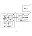
- FIG. 1 shows a block diagram of a configuration example of an electronic device to which a data receiving circuit according to the first embodiment of the present invention is applied.
- the electronic device 10 includes a display data supply device 20, a display driver 30, and a display panel 40.
- the display data supply device 20 includes a display data generation circuit 22, a data transmission circuit 24, a PLL circuit 26, and a transmission control unit 28.
- the display driver 30 includes a data receiving circuit 100 and a driving circuit 32.
- the function of the display data supply device 20 is realized by, for example, a so-called display controller, a central processing unit (Central Processing Unit), or the like.
- the display panel 40 is a liquid crystal panel or an organic EL panel in which a plurality of pixels are arranged in a matrix.
- the display driver 30 drives the pixels constituting the display panel 40 based on the display data supplied from the display data supply device 20, and displays an image corresponding to the display data.
- the display data generation circuit 22 In the display data supply device 20, the display data generation circuit 22 generates display data corresponding to the image displayed on the display panel 40.
- the PLL circuit 26 generates a clock corresponding to the step width of the pulse width modulation in the first embodiment and outputs it to the data transmission circuit 24.
- the data transmission circuit 24 performs a process of performing pulse width modulation on the display data generated by the display data generation circuit 22 using the clock from the PLL circuit 26 and transmitting the data after the pulse width modulation to the display driver 30. Do. Specifically, the data transmission circuit 24 performs pulse width modulation by modulating the change timing of transmission data with display data.
- the transmission control unit 28 controls the display data generation circuit 22, the data transmission circuit 24, and the PLL circuit 26.
- the data receiving circuit 100 performs a process of receiving data transmitted by the display data supply device 20.
- the data receiving circuit 100 detects the received data corresponding to the change timing of the received data based on the step width of the pulse width modulation in the first embodiment, and the detected received data is sent to the drive circuit 32 as the received display data. Output.
- the drive circuit 32 drives the display panel 40 based on the data received by the data receiving circuit 100.
- FIG. 2 is an explanatory diagram of pulse width modulation in the first embodiment.
- FIG. 2 shows an example in which pulse width modulation is performed on 4-bit display data in one cycle period.
- the rising edge of the data is extracted as the reference timing, and one cycle period is defined.
- a predetermined H level fixing period t0 that is always fixed to the H level is provided at the beginning of one cycle period, and a predetermined L level fixing period t1 that is always fixed to the L level is provided at the end of one cycle period. It is done.
- 15 falling edge positions are defined in two or more step sizes within a period excluding the H level fixed period t0 and the L level fixed period t1 within one cycle period. Including the positions of the falling edges where the H level fixed period t0 ends, the positions of 16 falling edges are defined within one cycle period.
- the position of each falling edge corresponds to each of 4-bit display data.
- the position of each falling edge is defined so that the step size becomes coarser as the distance from the reference timing increases. That is, 0 ⁇ tw 1 ⁇ tw 2 ⁇ tw 3 ⁇ ... ⁇ Tw 14 ⁇ tw 15 .
- the following equation is established. k is determined according to the delay accuracy when the timing of each falling edge is defined by delaying the timing of the immediately preceding falling edge.
- the position of the falling edge of the received data is defined by sequentially delaying the reference timing without using a complicated circuit such as a PLL circuit.
- the positions of 16 falling edges are defined with equal step sizes within a period excluding the H level fixed period t0 and the L level fixed period t1
- the falling edge becomes farther from the reference timing. Fluctuation increases. That is, the position of the falling edge close to the reference timing can be accurately defined, while the position of the falling edge far from the reference timing cannot be accurately defined due to element variation or the like.
- the position of each falling edge is defined so that the step size becomes coarser as the distance from the reference timing increases. Therefore, the position of the falling edge close to the reference timing can be accurately defined because the fluctuation is small. Further, the position of the falling edge that is far from the reference timing has a large step size, so that the position of the falling edge can be reliably defined even if there is element variation.
- the reference timing extracted from the reception data can be sequentially delayed to generate the capture timing of each falling edge. Therefore, without providing a PLL circuit, The position of the falling edge can be accurately defined. As a result, it is possible to realize multi-bit pulse width modulation.
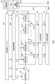
- FIG. 3 is a block diagram showing a configuration example of the data receiving circuit 100 according to the first embodiment.
- FIG. 3 shows a configuration example in the case of receiving reception data in which 4-bit display data is modulated by pulse width modulation having different step sizes.
- FIG. 3 shows a configuration in which data is captured at the positions of more than 16 falling edges for the purpose of error detection or the like, but data is captured at the positions of 16 falling edges at the minimum. If you can.
- the data receiving circuit 100 includes a delay circuit (data delay unit) 110, an output buffer 120, a capture timing generation circuit (capture timing generation unit) 130, a data capture circuit (data capture unit) 140, a pulse A width detection circuit (reception data detection unit) 150. Further, the data receiving circuit 100 includes a delay control register 160 and a delay control circuit 180.
- the delay circuit 110 delays the reception data D from the display data supply device 20.
- the delay circuit 110 has a configuration in which one or a plurality of delay elements are connected in cascade, and is configured such that the power supply voltage of each delay element can be changed. Therefore, the edge of the change point of the reception data D can be made sharp by setting the power supply voltage of the delay circuit 110 high, and the change point of the reception data D can be set by setting the power supply voltage of the delay circuit 110 low. Edges can be blunted.
- the output buffer 120 is provided between the delay circuit 110 and the capture timing generation circuit 130, buffers the output of the delay circuit 110, and outputs the buffered reception data to the capture timing generation circuit 130.
- the power supply voltage of the output buffer 120 can be changed. Therefore, by setting the power supply voltage of the output buffer 120 high, the edge of the change point of the reception data can be made sharp, and by setting the power supply voltage of the output buffer 120 low, the edge of the change point of the reception data Can be slowed down.
- the capture timing generation circuit 130 sequentially delays the output of the output buffer 120 (or the delay circuit 110) to generate a plurality of capture timings having two or more types of step sizes.
- the plurality of capture timings have smaller increments as the capture timing is closer to the reference timing.
- the capture timing generation circuit 130 includes a plurality of delay circuits DC0 to DC19, a termination circuit 132, and a plurality of clock buffers CB0 to CB19.
- the output of the output buffer 120 is connected to the input of the delay circuit DC0, each of the delay circuits DC0 to DC19 is connected in cascade, and the output of each delay circuit becomes each capture timing.
- a termination circuit 132 is connected to the output of the delay circuit DC19 at the final stage of the delay circuits DC0 to DC19 connected in cascade.
- the delay values of the delay circuits DC0 to DC19 are configured to be adjustable.
- the capacitance value of the termination circuit 132 is configured to be adjustable.
- the termination circuit 132 has a function of absorbing reflection of signals propagating through the delay circuits DC0 to DC19, and the delay value of each capture timing can be adjusted by changing the capacitance value.
- Each input of the plurality of clock buffers CB0 to CB19 is connected to the output of the corresponding delay circuit, and each of the plurality of clock buffers CB0 to CB19 captures the capture clocks CL0 to CL19 corresponding to the capture timing. Output to circuit 140.
- Each power supply voltage of the plurality of clock buffers CB0 to CB19 can be changed. Therefore, by setting the power supply voltage of the clock buffers CB0 to CB19 high, the edges of the transition points of the fetch clocks CL0 to CL19 can be made steep. By setting the power supply voltage of the clock buffers CB0 to CB19 low, the edges of the transition points of the fetch clocks CL0 to CL19 can be blunted.
- the data capture circuit 140 captures predetermined data at a plurality of capture timings generated by the capture timing generation circuit 130. That is, the data capture circuit 140 includes a plurality of flip-flops provided corresponding to each of a plurality of capture timings, and each flip-flop is predetermined based on a capture clock that changes at the corresponding capture timing. Import the data. Each flip-flop is initialized prior to reception of reception data D.
- the predetermined data is H level data
- the flip-flop after initialization holds L level data.
- the data fetch circuit 140 holds the H level data only in the flip-flops to which the fetch clock that changes to the H level among the fetch clocks CL0 to CL19 is input.
- the pulse width detection circuit 150 detects received data based on the acquired data DL0 to DL19. Specifically, the pulse width detection circuit 150 detects the received data corresponding to the detected pulse width by detecting the pulse width based on the captured data DL1 to DL16, and based on the captured data DL0 and DL17. An error is detected and an error detection result signal ERR is output. The reception data RD detected by the pulse width detection circuit 150 is supplied to the drive circuit 32 of the display driver 30.
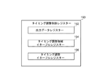
- the delay control register 160 includes a control for controlling at least one of the delay circuit 110, the output buffer 120, the delay circuits DC0 to DC19, the clock buffers CB0 to CB19, and the termination circuit 132 that constitute the capture timing generation circuit 130. Value is set.
- FIG. 4 shows an outline of the configuration of the delay control register 160.
- the delay control register 160 is a register that can be accessed by the display data supply device 20 or a CPU (not shown) (hereinafter, the display data supply device 20 or the like).
- the delay control register 160 includes a delay circuit control register 162, an output buffer control register 164, a capacitance value control register 166, a clock buffer control register 168, and a termination circuit control register 170.
- a control value corresponding to the power supply voltage of the delay circuit 110 is set as a first delay setting register by the display data supply device 20 or the like.
- the delay control circuit 180 outputs a control signal C1 corresponding to the control value set in the delay circuit control register 162, and sets the power supply voltage of the delay circuit 110 to a voltage corresponding to the control value.
- a control value corresponding to the power supply voltage of the output buffer 120 is set as the second delay setting register by the display data supply device 20 or the like.
- the delay control circuit 180 outputs a control signal C2 corresponding to the control value set in the output buffer control register 164, and sets the power supply voltage of the output buffer 120 to a voltage corresponding to the control value.
- the delay value can be independently adjusted for each of the delay circuit 110 and the output buffer 120.
- the delay value can be adjusted largely by the delay circuit 110, and the reception data having a sufficient amplitude level can be supplied to the capture timing generation circuit 130 by the output buffer 120.
- a control value corresponding to the delay values of the delay circuits DC0 to DC19 is set as the fifth delay setting register by the display data supply device 20 or the like.
- the capacitance value control register 166 is set with a control value corresponding to the capacitance value of the capacitive element constituting each of the delay circuits DC0 to DC19.
- the delay control circuit 180 outputs a control signal C3 corresponding to the control value set in the capacitance value control register 166, and simultaneously sets the capacitance value constituting each of the delay circuits DC0 to DC19 to the capacitance value corresponding to the control value. Set to.
- a control value corresponding to the power supply voltage of the clock buffers CB0 to CB19 is set as a third delay setting register by the display data supply device 20 or the like.
- the delay control circuit 180 outputs a control signal C4 corresponding to the control value set in the clock buffer control register 168, and simultaneously sets the power supply voltages of the clock buffers CB0 to CB19 to voltages corresponding to the control value.
- a control value corresponding to the capacitance value of the termination circuit 132 is set as the fourth delay setting register by the display data supply device 20 or the like.
- the delay control circuit 180 outputs a control signal C5 corresponding to the control value set in the termination circuit control register 170, and sets the capacitance value of the termination circuit 132 to a capacitance value corresponding to the control value.
- the rising edge of the received data is extracted as the reference timing.
- the reference timing is sequentially delayed by the delay circuit 110, the output buffer 120, the plurality of delay circuits DC0 to DC19, the clock buffers CB0 to CB19, and the termination circuit 132, and is generated as a capture clock corresponding to the capture timing.
- Each of the delay circuit 110, the output buffer 120, the plurality of delay circuits DC0 to DC19, the clock buffers CB0 to CB19, and the termination circuit 132 is configured to be able to adjust the delay value. Therefore, the capture timing and the capture clock corresponding to this can be adjusted.
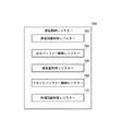
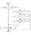
- FIG. 5 shows a flowchart of an operation example of the data receiving circuit 100 according to the first embodiment.
- the display data supply device 20 or the like sets a control value in each register constituting the delay control register 160 and adjusts the delay value (step S1, delay adjustment step). For example, the display data supply device 20 or the like repeatedly sets the control value in each register and verifies the detection result of the pulse width detection circuit 150. As a result, the optimum delay values of the delay circuit 110, the output buffer 120, the delay circuits DC0 to DC19, the clock buffers CB0 to CB19, and the termination circuit 132 are determined.
- the data receiving circuit 100 waits for data reception from the display data supply device 20 (step S2: N).
- the data reception circuit 100 When data from the display data supply device 20 is received (step S2: Y), the data reception circuit 100 generates a capture timing based on the received data input via the output buffer 120 (step S3, Capture timing generation step). Specifically, the data reception circuit 100 generates the capture timing by sequentially delaying the rising timing of the received data in the capture timing generation circuit 130. At this time, the capture timing generation circuit 130 outputs capture clocks CL0 to CL19 corresponding to the capture timing to the data capture circuit 140.
- the data receiving circuit 100 takes in the H level data based on the take-in clocks CL0 to CL19 in the plurality of flip-flops constituting the data take-in circuit 140 (step S4, data take-in step).
- the data acquisition circuit 140 outputs the data latched by the plurality of flip-flops to the pulse width detection circuit 150 as the acquisition data DL0 to DL19.
- the data receiving circuit 100 detects the received data in the pulse width detection circuit 150 based on the acquired data DL0 to DL19 acquired by the data acquiring circuit 140 at a plurality of acquisition timings (step S5, received data). Detection step). Thereafter, the data receiving circuit 100 ends a series of processing (end).
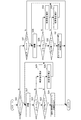
- FIG. 6 shows a circuit diagram of a detailed configuration example of the data receiving circuit 100 of FIG.
- the pulse width detection circuit 150, the delay control register 160, and the delay control circuit 180 in FIG. 3 are not shown. 6, parts that are the same as those in FIG. 3 are given the same reference numerals, and descriptions thereof are omitted as appropriate.
- the delay circuit 110 includes a plurality of buffers connected in cascade, and the power supply voltage of each buffer is set to a voltage set by the control signal C1.
- the capture timing generation circuit 130 includes a capacity initialization circuit 134 in addition to the delay circuits DC0 to DC19, the termination circuit 132, and the clock buffers CB0 to CB19.
- the delay circuit DC0 includes a resistance element having one end connected to the output of the output buffer 120 and the other end connected to one electrode of the capacitor, and the capacitor having the other electrode grounded. The other end of this resistance element is connected to the delay circuit DC1 at the next stage and to the input of the corresponding clock buffer CB0.
- the capacitive element constituting the delay circuit DC0 is a varactor diode, and is an element whose capacitance value is variable by changing the junction capacitance by a reverse bias voltage applied between the anode and the cathode. The capacitance value of this capacitive element is set by the control signal C3.
- Each of the delay circuits DC0 to DC19 has the same configuration.
- the termination circuit 132 includes a resistive element having one end connected to the output of the delay circuit DC19 and the other end connected to one electrode of the capacitive element, and the capacitive element having the other electrode grounded.
- This capacitive element is a varactor diode, and its capacitance value is set by a control signal C5.
- Capacitance initialization circuit 134 initializes the charges charged in the capacitive elements constituting each of delay circuits DC0 to DC19 prior to the output of each capture timing by capture timing generation circuit 130.
- Such a capacitance initialization circuit 134 includes a plurality of N-type MOSFETs (Metal-Oxide-Semiconductor Field-Effect Transistors) provided corresponding to the capacitance elements constituting each of the delay circuits DC0 to DC19. The source of each MOSFET is grounded, and the drain is connected to one electrode of the capacitive element constituting the corresponding delay circuit.
- N-type MOSFETs Metal-Oxide-Semiconductor Field-Effect Transistors
- a signal obtained by logically inverting the output of the delay circuit 110 is supplied to the gate of each MOSFET, and the MOSFET is turned on at the L level before the rising timing of the reception data D.
- the delay circuits DC0 to DC19 can delay the capture timing with high accuracy even when received data is repeatedly input.
- the data fetch circuit 140 includes flip-flops DF0 to DF19.
- Each of the flip-flops DF0 to DF19 includes a data input terminal D, a clock input terminal C, a data output terminal Q, and a reset input terminal R.
- the clock input terminal C of each of the flip-flops DF0 to DF19 is input with a clock taken in from the corresponding clock buffer.
- a high potential power source is connected to each data input terminal D of the flip-flops DF0 to DF19.
- Each of the flip-flops DF0 to DF19 takes in the H level data inputted to the data input terminal D at the rising edge of the signal inputted to the clock input terminal C, and outputs the taken data from the data output terminal Q as taken data. To do. Captured data DL0 to DL19 are output from data output terminals Q of flip-flops DF0 to DF19.
- the reset signal generated by the reset circuit 142 is input to the reset input terminals R of the flip-flops DF0 to DF19.
- the reset circuit 142 is a rise detection circuit, and outputs a pulse signal that changes to the L level in synchronization with the rise timing of the reception data D. Accordingly, the flip-flops DF0 to DF19 are initialized at the rising timing of the reception data D.
- FIG. 7 shows a circuit diagram of a configuration example of the pulse width detection circuit 150 of FIG. 7, parts that are the same as those in FIG. 3 are given the same reference numerals, and explanation thereof is omitted as appropriate.
- the pulse width detection circuit 150 in FIG. 7 detects an error based on the captured data DL0 and DL17 and outputs an error detection result signal ERR.
- Captured data DL0 and DL17 represent states before and after captured data DL1 to DL16 corresponding to data obtained by pulse width modulation of 4-bit display data.
- the pulse width detection circuit 150 includes an upper bit decoder 152.
- the pulse width detection circuit 150 performs an exclusive OR operation in the order of the acquisition data DL1, DL2, DL3,..., DL16 of the acquisition data DL1 to DL16 to thereby obtain the least significant bit RD of the 4-bit reception data. ⁇ 0> is generated.
- the upper bit decoder 152 generates each bit of the upper bits RD ⁇ 3: 1> of the received data of 4 bits by decoding the fetched data DL2 to DL16.
- the reception data RD ⁇ 3: 0> detected by the pulse width detection circuit 150 in this way is supplied to the drive circuit 32 of the display driver 30.
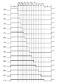
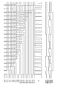
- FIG. 8 shows an example of a simulation result of the data receiving circuit 100 according to the first embodiment.
- FIG. 8 shows the received data D, the captured data DL0 to DL19, the detected received data RD ⁇ 3> to RD ⁇ 0>, and the error detection result signal ERR, with the time axis on the horizontal axis.
- the pulse width of the reception data D is increased by 0.5 ns for each cycle, and the acquisition data DL0 to DL19 and reception data RD are increased.
- ⁇ 3> to RD ⁇ 0> represent changes in the error detection result signal ERR.
- the reception data detected by the pulse width detection circuit 150 is increased when the pulse width of the reception data D is increased by a predetermined length every cycle.
- the value of RD ⁇ 3: 0> increases at a certain rate.
- the step size is reduced as it is closer to the reference timing, and the step size is increased as it is farther from the reference timing. Accordingly, when the pulse width of the reception data D is increased by a predetermined length for each cycle, the value of the reception data RD ⁇ 3: 0> detected by the pulse width detection circuit 150 is the case where the pulse width is small. When the pulse width is large compared to the above, it is difficult to increase.
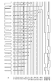
- FIG. 9 shows another example of the simulation result of the data receiving circuit 100 in the first embodiment.
- FIG. 9 shows the reception data D, the acquisition clocks CL0 to CL19, and the detected reception data RD ⁇ 3> to RD ⁇ 0> with the time axis on the horizontal axis.
- FIG. 9 is the same time axis as FIG. 8.
- the pulse width of the reception data D is increased by 0.5 ns per cycle, and the acquisition clocks CL0 to CL19, reception data This represents a change in RD ⁇ 3> to RD ⁇ 0>.
- the acquisition clocks CL0 to CL19 are It changes to H level at a constant rate.
- the plurality of flip-flops constituting the data capture circuit 140 can capture the H level data when the corresponding capture clock changes to the H level.
- the step size is reduced as it is closer to the reference timing, and the step size is increased as it is farther from the reference timing. Therefore, when the pulse width of the reception data D is increased by a predetermined length every cycle, the acquisition clocks CL0 to CL19 do not change to the H level at a constant rate. As shown in FIG. 9, among a plurality of flip-flops constituting data fetch circuit 140, a flip-flop to which a fetch clock that cannot sufficiently rise to H level is input cannot fetch H level data. . As a result, when the pulse width is larger than when the pulse width is small, the value of the reception data RD ⁇ 3: 0> detected by the pulse width detection circuit 150 is difficult to increase.
- display data is received by pulse width modulation in which the position of each falling edge is defined so that the step width becomes coarser as the distance from the reference timing increases.
- the position of the falling edge close to the reference timing can be accurately defined.
- the position of the falling edge far from the reference timing has a large step size, so that the position of the falling edge can be accurately defined even if there is element variation.
- the reference timing extracted from the received data can be sequentially delayed to generate the capture timing of each falling edge, so that the position of the falling edge can be accurately defined without providing a PLL circuit. be able to.
- the display data supply device 20 or the like determines the optimum delay value of each of the delay circuit 110, the output buffer 120, the plurality of delay circuits DC0 to DC19, the clock buffers CB0 to CB19, and the termination circuit 132.
- the embodiment according to the present invention is not limited to this.
- FIG. 10 is a block diagram showing a configuration example of the data receiving circuit according to the second embodiment of the present invention. 10 shows a configuration example in the case of receiving reception data in which 4-bit display data is modulated by pulse width modulation, as in FIG. 10, parts that are the same as those in FIG. 3 are given the same reference numerals, and descriptions thereof will be omitted as appropriate.
- the data receiving circuit 100a in the second embodiment includes a delay circuit 110, an output buffer 120, a capture timing generation circuit 130, a data capture circuit 140, a pulse width detection circuit 150, a delay control register 160, A delay control circuit 180a.
- the data receiving circuit 100a includes a timing adjustment control register 190 and a timing adjustment control circuit 200.
- the main difference between the configuration of the data receiving circuit 100 shown in FIG. 3 and the configuration of the data receiving circuit 100a in the second embodiment is that a timing adjustment control register 190 and a timing adjustment control circuit 200 are added.
- Such a data receiving circuit 100a can be provided in place of the data receiving circuit 100 in the display driver 30 of FIG.
- circuits similar to those in FIG. 3 can be configured in the same manner as those shown in FIG. 6 or FIG.
- timing adjustment control register 190 a control value for performing timing adjustment control is set by the display data supply device 20 or the like.
- FIG. 11 shows an outline of the configuration of the timing adjustment control register 190.
- the timing adjustment control register 190 is a register configured to be accessible by the display data supply device 20 or the like.
- the timing adjustment control register 190 includes an output data register 192, a timing adjustment forced enable register 194, and a timing adjustment enable register 196.
- the value of data transmitted from the display data supply device 20 to the data receiving circuit 100a is set by the display data supply device 20 or the like.
- the data receiving circuit 100a receives data obtained by pulse-width-modulating 4-bit data corresponding to the “(0) 16 ” value.
- the data receiving circuit 100 a receives data obtained by pulse width modulation of 4-bit data corresponding to the “(F) 16 ” value.
- timing adjustment forced enable register 194 an enable bit for instructing to perform timing adjustment control forcibly by the display data supply device 20 or the like is set.
- the data receiving circuit 100a forcibly performs control for adjusting the delay value for defining the timing of taking in the value set in the output data register 192. .
- timing adjustment enable register 196 an enable bit for instructing to perform timing adjustment control is set by the display data supply device 20 or the like.
- the data reception circuit 100a adjusts the delay value for defining the timing of taking in the value set in the output data register 192, for example, during the blanking period. Take control.
- the data receiving circuit 100a When the enable bit is set in the timing adjustment forced enable register 194 or the timing adjustment enable register 196 by the display data supply device 20 or the like, the data receiving circuit 100a performs the following timing adjustment control. As a result of the timing adjustment control, an optimum control value is set in the delay control register 160.
- FIG. 12 and FIG. 13 are flowcharts showing an operation example of the timing adjustment control in the second embodiment.
- FIG. 13 shows a flowchart of an operation example performed in step S11 of FIG.
- the flow shown in FIGS. 12 and 13 is desirably performed in step S1 as the delay adjustment step in FIG.
- the data receiving circuit 100a determines whether or not there is a forced calibration instruction in the timing adjustment control circuit 200 (step S10). Specifically, in step S10, the timing adjustment control circuit 200 determines whether or not an enable bit is set in the timing adjustment forced enable register 194. When the enable bit is set in the timing adjustment forced enable register 194 (step S10: Y), the timing adjustment control circuit 200 performs timing adjustment control (step S11), and ends a series of processing (end).
- step S12 the timing adjustment control circuit 200 determines whether or not there is a timing calibration instruction. Specifically, in step S12, the timing adjustment control circuit 200 determines whether an enable bit is set in the timing adjustment enable register 196. When the enable bit is set in the timing adjustment enable register 196 (step S12: Y), the timing adjustment control circuit 200 performs timing adjustment control during the blanking period. That is, the timing adjustment control circuit 200 waits until the vertical synchronization signal VSYNC becomes active (step S13: N).
- step S13: Y When the vertical synchronization signal VSYNC becomes active (step S13: Y), the timing adjustment control circuit 200 waits until the horizontal synchronization signal HSYNC for a predetermined number of lines becomes active (step S14: N). When the horizontal synchronization signals HSYNC for a predetermined number of lines become active (step S14: Y), the timing adjustment control circuit 200 performs timing adjustment control (step S11), and ends a series of processing (end).
- step S11 the timing adjustment control circuit 200 determines whether or not the value set in the output data register 192 is “(0) 16 ” (step S20).
- step S20 the timing adjustment control circuit 200 waits for a predetermined period (step S21). Within this predetermined period, data with the shortest pulse width is transmitted from the display data supply device 20, and the received data is detected by the pulse width detection circuit 150 of the data reception circuit 100a.
- the timing adjustment control circuit 200 determines the presence or absence of an error based on the error detection result signal ERR from the pulse width detection circuit 150 (step S22). When it is determined that there is no error based on the error detection result signal ERR (step S22: Y), the timing adjustment control circuit 200 determines whether the pulse width is “0” based on the reception data RD ⁇ 3: 0>. It is determined whether or not (step S23). When the pulse width is “0” (step S23: Y), the timing adjustment control circuit 200 sets a control value corresponding to the current delay value in the delay circuit control register 162 (step S24), and a series of processes End (end).
- step S22 When it is determined in step S22 that there is an error based on the error detection result signal ERR (step S22: N), the timing adjustment control circuit 200 increases the control value set in the delay circuit control register 162 (step S22). S25), the process returns to step S21.
- step S23 When the pulse width is not “0” in step S23 (step S23: N), the timing adjustment control circuit 200 decreases the control value set in the delay circuit control register 162 (step S26), and returns to step S21.
- step S20 N
- the timing adjustment control circuit 200 determines whether the value set in the output data register 192 is “(F) 16 ”. It is determined whether or not (step S27).
- step S27: Y the timing adjustment control circuit 200 waits for a predetermined period (step S28). Within this predetermined period, the data with the longest pulse width is transmitted from the display data supply device 20, and the received data is detected by the pulse width detection circuit 150 of the data reception circuit 100a.
- the timing adjustment control circuit 200 determines the presence or absence of an error based on the error detection result signal ERR from the pulse width detection circuit 150 (step S29). When it is determined that there is no error based on the error detection result signal ERR (step S29: Y), the timing adjustment control circuit 200 determines whether the pulse width is “15” based on the reception data RD ⁇ 3: 0>. It is determined whether or not (step S30). When the pulse width is “15” (step S30: Y), the timing adjustment control circuit 200 sets the control value corresponding to the current delay value to the output buffer control register 164, the capacitance value control register 166, and the clock buffer. The control register 168 and the termination circuit control register 170 are set (step S31), and the series of processing ends (end).
- step S29 When it is determined in step S29 that there is an error based on the error detection result signal ERR (step S29: N), the timing adjustment control circuit 200 outputs the output buffer control register 164, the capacitance value control register 166, and the clock buffer control. The control value set in either the register 168 or the termination circuit control register 170 is increased (step S32), and the process returns to step S28.
- step S30 N
- the timing adjustment control circuit 200 outputs the output buffer control register 164, the capacitance value control register 166, the clock buffer control register 168, and the termination circuit control register.
- the control value set to any one of 170 is decreased (step S33), and the process returns to step S28.
- step S27: N the timing adjustment control circuit 200 ends a series of processing (end).
- the first data obtained by performing the pulse width modulation on “(0) 16 ” in which the pulse width of the reception data is the shortest, and “(F) in which the pulse width of the reception data is the longest. 16 ” is used to adjust the delay value of the delay means of the data receiving circuit 100 a using the second data obtained by pulse width modulation of“ 16 ”.
- the delay means of the data receiving circuit 100a includes at least one of a delay circuit 110, an output buffer 120, delay circuits DC0 to DC19, clock buffers CB0 to CB19, and a termination circuit 132.
- the end timing of the H level fixed period t0 can be defined by adjusting the delay value based on the reception data with the shortest pulse width.
- the lower timing of the L level fixed period t1 can be defined by adjusting the delay value based on the reception data having the shortest pulse width.
- the delay circuit 110, the output buffer 120, the delay circuits DC0 to DC19, the clock buffers CB0 to CB19, and the termination circuit 132 are forcibly or during a predetermined period.
- the control value can be determined.
- an optimum control value is always set even during operation, and multi-bit pulse width modulated data can be received stably. Therefore, even at a frequency exceeding the measurement limit of the measuring device, a large amount of display data can be transmitted / received at high speed at a low cost.
- FIG. 14 shows a configuration example of the delay circuit in the modified example of the first embodiment or the second embodiment.
- the delay circuit 110 in the present modification includes a plurality of first delay elements DS1, a plurality of second delay elements DS2, and an output selection unit SEL.
- the plurality of first delay elements DS1 are connected in cascade, and the reception data D from the display data supply device 20 is input to the input of the first delay element DS1 in the first stage, and each first delay element DS1.
- the output of each first delay element DS1 is also connected to the output selection unit SEL via each second delay element DS2.
- the second delay element DS2 is connected to the high-potential side power supply via any one of a plurality of resistance elements having different resistance values, and can adjust the delay time of the rise of the output signal. ing.
- the second delay element DS2 is connected to the low-potential-side power supply via any one of a plurality of resistance elements having different resistance values, and can adjust the delay time of the fall of the output signal. It is like that.
- the delay control circuit 180 outputs a control signal C1 corresponding to the control value set in the delay circuit control register 162 to the plurality of second delay elements DS2 and the output selection unit SEL.
- Each second delay element DS2 is connected to a high potential power source and a low potential power source via a resistance element selected based on the control signal C1.
- the output selection unit SEL selects any one of the outputs of the plurality of first delay elements DS1 and the plurality of second delay elements DS2 based on the control signal C1, and passes through the selected path.
- the signal is output to the output buffer 120 as an output signal.
- the delay value can be finely adjusted with higher accuracy than the delay circuit having the configuration shown in FIG.
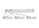
- FIG. 15 is an explanatory diagram of display data supplied from the display data supply device 20 of FIG. 1 to the display driver 30.
- the display data is composed of 12 bits D11 to D0, where D11 is the upper bit side and D0 is the lower bit side.
- the display data supply device 20 divides the display data into 4 bits and performs pulse width modulation on the divided data.
- the upper bit side contributes more to the change in luminance than the lower bit side. Therefore, as shown in FIG. 15, the first group is D11, D8, D5, D2, the second group is D10, D7, D4, D1, the third group is D9, D6, D3, D0,
- the upper bits of the group are D11, D10, and D9. Therefore, when 4-bit data of each group is subjected to pulse width modulation, even if a bit error occurs due to noise or the like near the falling edge of the pulse, the lower bits are not detected, and the pulse width corresponding to the upper bits has a high probability. Can be detected. Therefore, even when the display panel 40 is driven using such data, the influence on the display image is small.
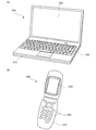
- the display driver provided with the data receiving circuit in any of the above embodiments or the modifications thereof can be applied to, for example, the following electronic apparatus.
- FIGS. 16A and 16B are perspective views showing the configuration of an electronic apparatus having a display driver provided with a data receiving circuit in any of the above-described embodiments or modifications thereof.
- FIG. 16A illustrates a perspective view of a configuration of a mobile personal computer.
- FIG. 16B illustrates a perspective view of a structure of a mobile phone.
- a personal computer 500 shown in FIG. 16A includes a main body portion 510 and a display portion 520.
- the display unit 520 includes a display driver including the data receiving circuit in any one of the above-described embodiments or modifications thereof.
- the main body 510 is provided with a keyboard 530. Operation information via the keyboard 530 is analyzed by a control unit (not shown), and an image is displayed on the display unit 520 in accordance with the operation information. Since the display portion 520 can transmit and receive signals at high speed, it is possible to provide the personal computer 500 capable of displaying very high definition at a low cost.
- a cellular phone 600 illustrated in FIG. 16B includes a main body portion 610 and a display portion 620.
- the display unit 620 includes a display driver including the data receiving circuit in any one of the above-described embodiments or modifications thereof.
- the main body 610 is provided with a key 630. Operation information via the key 630 is analyzed by a control unit (not shown), and an image is displayed on the display unit 620 according to the operation information. Since the display portion 620 can transmit and receive signals at high speed, it is possible to provide the mobile phone 600 capable of displaying very high definition at low cost.
- the electronic device on which the display driver including the data receiving circuit in any of the above-described embodiments or modifications thereof is mounted is not limited to those shown in FIGS. Absent.
- PDAs personal digital assistants
- digital still cameras televisions, video cameras, car navigation devices, pagers, electronic notebooks, electronic papers, calculators, word processors, workstations, videophones, POS (Point of sale systems)
- POS Point of sale systems
- Devices such as terminals, printers, scanners, copiers, video players and touch panels.
- the above-described electronic device can contribute to realization of a large capacity and high-speed processing by accurately receiving a high-speed signal.
- the data receiving circuit, the electronic device, the data receiving method, and the like according to the present invention have been described based on any one of the above-described embodiments or modifications thereof. It is not limited to examples.
- the present invention can be implemented in various modes without departing from the gist thereof, and the following modifications are possible.
- the data receiving circuit has been described as outputting captured data DL0 to DL19, but the present invention is not limited to this.
- the data receiving circuit may have a configuration for outputting the captured data DL0 to DL17.
- the data receiving circuit may be configured to output the fetched data DL1 to DL16.
- pulse width modulation is mainly performed on 4-bit display data.
- the present invention is not limited to this.
- the present invention can be applied to a device that performs pulse width modulation on display data of a plurality of bits other than 4 bits.
- the present invention is not limited to this.
- the present invention can also be applied to the detection of the L level width.
- the step size is increased as the capture timing is closer to the reference timing. Then, the width of the L level may be detected based on the rising edge of the received data that is the end timing of the L level fixed period shown in FIG.
- the present invention has been described as a data receiving circuit, an electronic device, a data receiving method, and the like, but the present invention is not limited to this.
- a program in which the processing procedure of the data receiving method according to the present invention is described, and a recording medium on which the program is recorded may be used.
- DESCRIPTION OF SYMBOLS 10 ... Electronic device, 20 ... Display data supply apparatus, 22 ... Display data generation circuit, 24 ... Data transmission circuit, 26 ... PLL circuit, 28 ... Transmission control part, 30 ... Display driver, 32 ... Drive circuit, 40 ... Display panel , 100, 100a ... data receiving circuit, 110 ... delay circuit (data delay unit) 120 ... output buffer, 130 ... capture timing generation circuit (capture timing generation unit), 132 ... termination circuit, 134 ... capacity initialization circuit, 140 ... Data acquisition circuit (data acquisition unit), 142 ... Reset circuit, 150 ... Pulse width detection circuit (reception data detection unit), 152 ... Upper bit decoder, 160 ... Delay control register, 162 ...
- Delay circuit control register ( First delay setting register), 164... Output buffer control register (second delay setting register) 166... Capacitance value control register (third delay setting register), 168... Clock buffer control register (fourth delay setting register), 170.
- Termination circuit control register (fifth delay setting register), 180, 180a.
- Delay control circuit 190 ... Timing adjustment control register, 192 ... Output data register, 194 ... Timing adjustment forced enable register, 196 ... Timing adjustment enable register, 200 ... Timing adjustment control circuit, C1-C5 ... Control signal, CB0-CB19 ... Clock buffer, CL0 to CL19 ... Capture clock, D, RD ... Receive data, DC0 to DC19 ...
- Delay circuit DF0 to DF19 ... Flip-flop, DL0 to DL19 ... Capture data, DS1 ... First delay element, DS2 ... Second Extension elements, ERR ... error detection result signal, t0 ... H level fixed duration, t1 ... L level fixed period, tw 0 ⁇ tw 15 ... stride, SEL ... output selection unit.
Landscapes
- Engineering & Computer Science (AREA)
- Computer Networks & Wireless Communication (AREA)
- Signal Processing (AREA)
- Physics & Mathematics (AREA)
- Spectroscopy & Molecular Physics (AREA)
- Dc Digital Transmission (AREA)
Applications Claiming Priority (2)
| Application Number | Priority Date | Filing Date | Title |
|---|---|---|---|
| JP2012-052625 | 2012-03-09 | ||
| JP2012052625A JP5987371B2 (ja) | 2012-03-09 | 2012-03-09 | データ受信回路、電子機器、及びデータ受信方法 |
Publications (1)
| Publication Number | Publication Date |
|---|---|
| WO2013132875A1 true WO2013132875A1 (fr) | 2013-09-12 |
Family
ID=49116364
Family Applications (1)
| Application Number | Title | Priority Date | Filing Date |
|---|---|---|---|
| PCT/JP2013/001542 Ceased WO2013132875A1 (fr) | 2012-03-09 | 2013-03-08 | Circuit de réception de données, appareil électronique et procédé de réception de données |
Country Status (2)
| Country | Link |
|---|---|
| JP (1) | JP5987371B2 (fr) |
| WO (1) | WO2013132875A1 (fr) |
Cited By (2)
| Publication number | Priority date | Publication date | Assignee | Title |
|---|---|---|---|---|
| DE102014201807B3 (de) * | 2014-01-31 | 2015-02-26 | Universität Rostock | Verfahren und System zur Übertragung von Daten |
| CN109407999A (zh) * | 2018-11-16 | 2019-03-01 | 郑州云海信息技术有限公司 | 一种信号矫正方法、系统及装置 |
Citations (3)
| Publication number | Priority date | Publication date | Assignee | Title |
|---|---|---|---|---|
| JPS63190457A (ja) * | 1986-10-02 | 1988-08-08 | Yazaki Corp | シリアルデ−タ伝送装置 |
| US6463092B1 (en) * | 1998-09-10 | 2002-10-08 | Silicon Image, Inc. | System and method for sending and receiving data signals over a clock signal line |
| JP2007129735A (ja) * | 2005-10-31 | 2007-05-24 | Silicon Image Inc | Dcバランスコントロールを有するクロックエッジ変調されたシリアルリンク |
-
2012
- 2012-03-09 JP JP2012052625A patent/JP5987371B2/ja not_active Expired - Fee Related
-
2013
- 2013-03-08 WO PCT/JP2013/001542 patent/WO2013132875A1/fr not_active Ceased
Patent Citations (3)
| Publication number | Priority date | Publication date | Assignee | Title |
|---|---|---|---|---|
| JPS63190457A (ja) * | 1986-10-02 | 1988-08-08 | Yazaki Corp | シリアルデ−タ伝送装置 |
| US6463092B1 (en) * | 1998-09-10 | 2002-10-08 | Silicon Image, Inc. | System and method for sending and receiving data signals over a clock signal line |
| JP2007129735A (ja) * | 2005-10-31 | 2007-05-24 | Silicon Image Inc | Dcバランスコントロールを有するクロックエッジ変調されたシリアルリンク |
Cited By (3)
| Publication number | Priority date | Publication date | Assignee | Title |
|---|---|---|---|---|
| DE102014201807B3 (de) * | 2014-01-31 | 2015-02-26 | Universität Rostock | Verfahren und System zur Übertragung von Daten |
| CN109407999A (zh) * | 2018-11-16 | 2019-03-01 | 郑州云海信息技术有限公司 | 一种信号矫正方法、系统及装置 |
| CN109407999B (zh) * | 2018-11-16 | 2022-03-08 | 郑州云海信息技术有限公司 | 一种信号矫正方法、系统及装置 |
Also Published As
| Publication number | Publication date |
|---|---|
| JP5987371B2 (ja) | 2016-09-07 |
| JP2013187793A (ja) | 2013-09-19 |
Similar Documents
| Publication | Publication Date | Title |
|---|---|---|
| US9589524B2 (en) | Display device and method for driving the same | |
| US7600061B2 (en) | Data transfer control device and electronic instrument | |
| US10950197B2 (en) | Data driver, display device having the same, and method of driving the display device | |
| CN108665840B (zh) | 显示器驱动设备 | |
| CN107769906B (zh) | 半导体装置、数据传输系统以及半导体装置的工作方法 | |
| EP3333843A1 (fr) | Registre à décalage, circuit de commande de grille, procédé de commande de panneau d'affichage, et dispositif d'affichage | |
| CN101996684B (zh) | 移位寄存器及触控装置 | |
| TWI453715B (zh) | 自動調整訊號偏移之裝置 | |
| CN112216239B (zh) | 源极驱动器和显示装置 | |
| KR102502236B1 (ko) | 클락 데이터 복구 회로, 이를 포함하는 장치 및 클락 데이터 복구 방법 | |
| CN105551445A (zh) | 伽玛电压生成电路以及包括其的液晶显示装置 | |
| US20150170592A1 (en) | Display devices with enhanced driving capability and reduced circuit area of driving circuit | |
| US11996065B2 (en) | Display driving circuit, display device including the same, and method of operating the same | |
| US20070211010A1 (en) | Display system capable of automatic de-skewing and method of driving the same | |
| US20150213779A1 (en) | Display driving circuit | |
| KR102525544B1 (ko) | 표시 장치 및 이의 구동 방법 | |
| US7876130B2 (en) | Data transmitting device and data receiving device | |
| US20150049848A1 (en) | Receiver circuit, communication system, electronic device, and method for controlling receiver circuit | |
| JP5987371B2 (ja) | データ受信回路、電子機器、及びデータ受信方法 | |
| KR20100129153A (ko) | 액정표시장치 | |
| KR101958654B1 (ko) | 도트 인버젼 액정표시장치 | |
| US20100110064A1 (en) | Source driver and liquid crystal display device having the same | |
| CN100429694C (zh) | 图像数据处理设备和图像数据处理方法 | |
| CN102376239A (zh) | 显示装置的像素电路 | |
| KR100932138B1 (ko) | 데이터 송신 장치 |
Legal Events
| Date | Code | Title | Description |
|---|---|---|---|
| 121 | Ep: the epo has been informed by wipo that ep was designated in this application |
Ref document number: 13758560 Country of ref document: EP Kind code of ref document: A1 |
|
| DPE1 | Request for preliminary examination filed after expiration of 19th month from priority date (pct application filed from 20040101) | ||
| NENP | Non-entry into the national phase |
Ref country code: DE |
|
| 122 | Ep: pct application non-entry in european phase |
Ref document number: 13758560 Country of ref document: EP Kind code of ref document: A1 |