WO2013136755A1 - Dispositif d'alimentation en énergie électrique de dispositif de charge par induction - Google Patents
Dispositif d'alimentation en énergie électrique de dispositif de charge par induction Download PDFInfo
- Publication number
- WO2013136755A1 WO2013136755A1 PCT/JP2013/001540 JP2013001540W WO2013136755A1 WO 2013136755 A1 WO2013136755 A1 WO 2013136755A1 JP 2013001540 W JP2013001540 W JP 2013001540W WO 2013136755 A1 WO2013136755 A1 WO 2013136755A1
- Authority
- WO
- WIPO (PCT)
- Prior art keywords
- power
- power supply
- circuit
- switching elements
- control circuit
- Prior art date
- Legal status (The legal status is an assumption and is not a legal conclusion. Google has not performed a legal analysis and makes no representation as to the accuracy of the status listed.)
- Ceased
Links
Images


Classifications
-
- H—ELECTRICITY
- H02—GENERATION; CONVERSION OR DISTRIBUTION OF ELECTRIC POWER
- H02M—APPARATUS FOR CONVERSION BETWEEN AC AND AC, BETWEEN AC AND DC, OR BETWEEN DC AND DC, AND FOR USE WITH MAINS OR SIMILAR POWER SUPPLY SYSTEMS; CONVERSION OF DC OR AC INPUT POWER INTO SURGE OUTPUT POWER; CONTROL OR REGULATION THEREOF
- H02M1/00—Details of apparatus for conversion
- H02M1/42—Circuits or arrangements for compensating for or adjusting power factor in converters or inverters
- H02M1/4208—Arrangements for improving power factor of AC input
- H02M1/4225—Arrangements for improving power factor of AC input using a non-isolated boost converter
-
- H—ELECTRICITY
- H02—GENERATION; CONVERSION OR DISTRIBUTION OF ELECTRIC POWER
- H02J—ELECTRIC POWER NETWORKS; CIRCUIT ARRANGEMENTS OR SYSTEMS FOR SUPPLYING OR DISTRIBUTING ELECTRIC POWER; SYSTEMS FOR STORING ELECTRIC ENERGY
- H02J50/00—Circuit arrangements or systems for wireless supply or distribution of electric power
- H02J50/10—Circuit arrangements or systems for wireless supply or distribution of electric power using inductive coupling
-
- H—ELECTRICITY
- H02—GENERATION; CONVERSION OR DISTRIBUTION OF ELECTRIC POWER
- H02J—ELECTRIC POWER NETWORKS; CIRCUIT ARRANGEMENTS OR SYSTEMS FOR SUPPLYING OR DISTRIBUTING ELECTRIC POWER; SYSTEMS FOR STORING ELECTRIC ENERGY
- H02J50/00—Circuit arrangements or systems for wireless supply or distribution of electric power
- H02J50/10—Circuit arrangements or systems for wireless supply or distribution of electric power using inductive coupling
- H02J50/12—Circuit arrangements or systems for wireless supply or distribution of electric power using inductive coupling of the resonant type
-
- H—ELECTRICITY
- H02—GENERATION; CONVERSION OR DISTRIBUTION OF ELECTRIC POWER
- H02J—ELECTRIC POWER NETWORKS; CIRCUIT ARRANGEMENTS OR SYSTEMS FOR SUPPLYING OR DISTRIBUTING ELECTRIC POWER; SYSTEMS FOR STORING ELECTRIC ENERGY
- H02J50/00—Circuit arrangements or systems for wireless supply or distribution of electric power
- H02J50/80—Circuit arrangements or systems for wireless supply or distribution of electric power involving the exchange of data, concerning supply or distribution of electric power, between transmitting devices and receiving devices
-
- H—ELECTRICITY
- H02—GENERATION; CONVERSION OR DISTRIBUTION OF ELECTRIC POWER
- H02J—ELECTRIC POWER NETWORKS; CIRCUIT ARRANGEMENTS OR SYSTEMS FOR SUPPLYING OR DISTRIBUTING ELECTRIC POWER; SYSTEMS FOR STORING ELECTRIC ENERGY
- H02J7/00—Circuit arrangements for charging or discharging batteries or for supplying loads from batteries
- H02J7/40—Circuit arrangements for charging or discharging batteries or for supplying loads from batteries characterised by the exchange of charge or discharge related data
- H02J7/42—Circuit arrangements for charging or discharging batteries or for supplying loads from batteries characterised by the exchange of charge or discharge related data with electronic devices having internal batteries, e.g. mobile phones
-
- H—ELECTRICITY
- H02—GENERATION; CONVERSION OR DISTRIBUTION OF ELECTRIC POWER
- H02M—APPARATUS FOR CONVERSION BETWEEN AC AND AC, BETWEEN AC AND DC, OR BETWEEN DC AND DC, AND FOR USE WITH MAINS OR SIMILAR POWER SUPPLY SYSTEMS; CONVERSION OF DC OR AC INPUT POWER INTO SURGE OUTPUT POWER; CONTROL OR REGULATION THEREOF
- H02M1/00—Details of apparatus for conversion
- H02M1/14—Arrangements for reducing ripples from DC input or output
-
- H—ELECTRICITY
- H02—GENERATION; CONVERSION OR DISTRIBUTION OF ELECTRIC POWER
- H02M—APPARATUS FOR CONVERSION BETWEEN AC AND AC, BETWEEN AC AND DC, OR BETWEEN DC AND DC, AND FOR USE WITH MAINS OR SIMILAR POWER SUPPLY SYSTEMS; CONVERSION OF DC OR AC INPUT POWER INTO SURGE OUTPUT POWER; CONTROL OR REGULATION THEREOF
- H02M1/00—Details of apparatus for conversion
- H02M1/0067—Converter structures employing plural converter units, other than for parallel operation of the units on a single load
- H02M1/007—Plural converter units in cascade
-
- Y—GENERAL TAGGING OF NEW TECHNOLOGICAL DEVELOPMENTS; GENERAL TAGGING OF CROSS-SECTIONAL TECHNOLOGIES SPANNING OVER SEVERAL SECTIONS OF THE IPC; TECHNICAL SUBJECTS COVERED BY FORMER USPC CROSS-REFERENCE ART COLLECTIONS [XRACs] AND DIGESTS
- Y02—TECHNOLOGIES OR APPLICATIONS FOR MITIGATION OR ADAPTATION AGAINST CLIMATE CHANGE
- Y02B—CLIMATE CHANGE MITIGATION TECHNOLOGIES RELATED TO BUILDINGS, e.g. HOUSING, HOUSE APPLIANCES OR RELATED END-USER APPLICATIONS
- Y02B70/00—Technologies for an efficient end-user side electric power management and consumption
- Y02B70/10—Technologies improving the efficiency by using switched-mode power supplies [SMPS], i.e. efficient power electronics conversion e.g. power factor correction or reduction of losses in power supplies or efficient standby modes
Definitions
- the present disclosure relates to a non-contact charging device that charges a secondary battery mounted on, for example, an electric propulsion vehicle (electric vehicle or hybrid vehicle) in a non-contact manner.
- a non-contact charging device that charges a secondary battery mounted on, for example, an electric propulsion vehicle (electric vehicle or hybrid vehicle) in a non-contact manner.
- Such a non-contact power transmission technique eliminates the need for wiring for connecting the power feeding device and the power receiving device, so that the user is saved from the trouble of connection, and there is no fear of electric leakage or electric shock during rainy weather.
- each of the power feeding device and the power receiving device includes a resonance unit that resonates an AC signal, thereby reducing the restriction on the positional relationship between the power feeding device and the power receiving device (for example, see Patent Document 1).
- the present disclosure provides a power feeding device for a non-contact charging device that can reduce ripples generated in an output, can be reduced in size and cost, and can suppress power feeding loss as much as possible. This is the issue.
- the power supply device of the non-contact charging device that supplies power to the power receiving device in a non-contact manner is connected to the power factor improvement circuit that converts the AC power source into DC and improves the power factor, and the output terminal of the power factor improvement circuit.
- an inverter circuit that generates an alternating current signal by switching each of the switching elements using the voltage of the smoothing capacitor as a power source, and is connected to an output terminal of the inverter circuit. And supplying a power generated between the first inductor and a second inductor provided in the power receiving device to the power receiving device based on the AC signal.
- a power supply unit and when power is supplied from the power supply unit to the power receiving device, the energization rate of each switching element of the inverter circuit is determined.
- a control circuit for modulating in synchronization with the alternating current power supply the control circuit increases or decreases the width of the modulation of the duty ratio is used to control the plurality of switching elements so that the asymmetrical.
- the ripple generated in the output can be reduced, the size and cost can be reduced, and the power feeding loss can be suppressed.
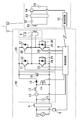
- FIG. 1 is a circuit diagram showing a non-contact charging apparatus according to Embodiment 1.
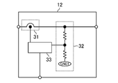
- FIG. FIG. 2 is a circuit diagram showing a configuration example of the input detection unit shown in FIG.
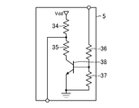
- FIG. 3 is a circuit diagram showing a configuration example of the synchronization signal generator shown in FIG.
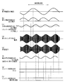
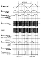
- FIG. 4 is a waveform diagram of each part of the conventional power transmission system for comparison with the non-contact charging apparatus of FIG.
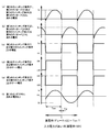
- FIG. 5 is a waveform diagram of each part in the contactless charging apparatus of FIG. 1 when the energization rate of the inverter circuit shown in FIG. 1 is changed.
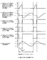
- FIG. 6 is an enlarged view of an operation waveform diagram of the inverter circuit when the input power is high.
- FIG. 7 is an enlarged view of an operation waveform diagram of the inverter circuit when the input power is low.
- FIG. 8 is a diagram illustrating the relationship between the input current and the ⁇ energization rate of the power feeding device illustrated in FIG. 1.
- FIG. 9 is a diagram illustrating a relationship between the input power and the energization rate of the power supply apparatus illustrated in FIG.
- the present disclosure is a power supply device for a non-contact charging device that supplies power to a power receiving device in a non-contact manner, which converts an AC power source into a direct current and improves a power factor, and an output of the power factor correction circuit
- a smoothing capacitor connected to the end, and an inverter circuit that has a plurality of switching elements and generates an AC signal by switching each switching element using the voltage of the smoothing capacitor as a power source, and is connected to the output end of the inverter circuit
- a power supply unit that has a resonance capacitor and a first inductor and supplies power received between the first inductor and the second inductor provided in the power receiving device to the power receiving device based on an AC signal
- a control circuit that modulates the energization rate of each switching element of the inverter circuit in synchronization with the AC power supply when power is supplied from the power supply unit to the power receiving device.
- Comprising a control circuit is to increase or decrease the width of the modulation of the duty factor controls
- control circuit increases the modulation amount of the energization rate of the plurality of switching elements as the input from the AC power supply to the power supply apparatus increases.
- control circuit is configured so that the pattern for modulating the energization rate is a substantially sine wave having a frequency twice that of the AC power supply.
- This configuration can reduce the output ripple of the power feeding device even in the case of feed-forward control instead of feedback control that requires high detection accuracy.
- the ripple generated in the output of the power receiving device can be reduced, and the power supply device does not need a component for detecting the output of the first inductor or a component for detecting the voltage of the smoothing capacitor. Become. Therefore, the number of parts of the power feeding device is reduced, and the power feeding device can be reduced in size and cost.
- (Embodiment 1) 1 is a circuit diagram of a contactless charging apparatus according to Embodiment 1.
- FIG. 1 is a circuit diagram of a contactless charging apparatus according to Embodiment 1.
- the non-contact charging device 1 includes a power feeding device 2 installed in a parking space, for example, and a power receiving device 50 mounted on an electric propulsion vehicle, for example.
- the power supply device 2 includes a commercial power supply 3, a first rectifier circuit 4, a synchronization signal generation unit 5, a control circuit 6 on the power supply device 2 side (hereinafter simply referred to as “control circuit 6”), a power supply unit 9, and a power factor improvement.
- control circuit 6 a control circuit 6 on the power supply device 2 side
- a circuit 10 and an inverter circuit 20 are included.
- the power receiving device 50 includes a second inductor 51, a second resonant capacitor 52, a second rectifier circuit 53, a load (for example, a battery) 18, a power receiving detection unit 54, and a control circuit 55 on the power receiving device 50 side (hereinafter simply referred to as “power receiving device 50”). (Referred to as “control circuit 55”).
- the power factor correction circuit 10 is a circuit that improves the power factor of the commercial power source 3.
- the power factor improvement circuit 10 includes a bypass capacitor 11, an input detection unit 12, a choke coil 13, a first switching element 14 (MOSFET: metal-oxide-semiconductor field-effect transistor) in the present embodiment, A first diode 15 and a smoothing capacitor (electrolytic capacitor) 16 are included.
- MOSFET metal-oxide-semiconductor field-effect transistor
- the commercial power source 3 is, for example, a 200V commercial power source that is a low-frequency AC power source, and is connected to the input terminal of the first rectifier circuit 4 including a bridge diode and an input filter.
- the high potential side terminal of the bypass capacitor 11 and the input detection unit 12 are connected to the output terminal on the high potential side (positive electrode side) of the first rectifier circuit 4.
- the output terminal of the input detection unit 12 is connected to the input side terminal of the choke coil 13.
- the high potential side terminal (drain) of the first switching element 14 is connected to a connection line between the output side terminal of the choke coil 13 and the anode of the first diode 15.
- the low potential side (negative electrode side) output terminal of the first rectifier circuit 4 includes a low potential side terminal of the bypass capacitor 11, a low potential side terminal (source) of the first switching element 14, and a low potential of the smoothing capacitor 16. Side terminals are connected.
- the high potential side terminal of the smoothing capacitor 16 is connected to the cathode of the first diode 15.
- the output voltage of the first rectifier circuit 4 is input as a DC power source to the power factor correction circuit 10 configured as described above. Specifically, the voltage fluctuation of the output voltage of the first rectifier circuit 4 is first suppressed by the bypass capacitor 11. Then, by the on / off operation of the first switching element 14 and the choke coil 13, the output voltage of the first rectifier circuit 4 is boosted to an arbitrary voltage which is a DC voltage having a value larger than the peak value. This boosted voltage is supplied to both ends of the smoothing capacitor 16 and smoothed.
- a MOSFET having a high switching speed is used as the first switching element 14 in order to increase the power factor improvement effect by operating the power factor improvement circuit 10 at a high frequency.
- a diode may be attached to the MOSFET in the opposite direction. However, even if this diode is not provided, it does not affect the basic operation of the present embodiment, and is not shown in the figure.
- the output voltage of the smoothing capacitor 16 is supplied between the input terminals of the inverter circuit 20.
- the input terminal of the inverter circuit 20 is connected to the output terminal of the power factor correction circuit 10, that is, both ends of the smoothing capacitor 16. Both ends of the smoothing capacitor 16 are connected in parallel with the second and third switching elements 21 and 23 connected in series and the fourth and fifth switching elements 26 and 28 connected in series. .
- Second and third diodes 22 and 24 are connected in antiparallel to the second and third switching elements 21 and 23, respectively. Specifically, the high potential side terminal (collector) of the switching element and the cathode of the diode are connected.
- a snubber capacitor 25 is connected to the third switching element 23 in parallel. Note that the snubber capacitor 25 may be connected to the second switching element 21 in parallel.
- fourth and fifth diodes 27 and 29 are connected in antiparallel to the fourth and fifth switching elements 26 and 28, respectively.
- the high potential side terminal (collector) of the switching element and the cathode of the diode are connected.
- a snubber capacitor 30 is connected to the fifth switching element 28 in parallel. Note that the snubber capacitor 30 may be connected to the fourth switching element 26 in parallel.
- the power supply unit 9 is connected to a connection line between the second switching element 21 and the third switching element 23 and a connection line between the fourth switching element 26 and the fifth switching element 28.
- the inverter circuit 20 generates an AC signal by switching the second to fifth switching elements 21, 23, 26, and outputs it to the power supply unit 9.
- the power supply unit 9 can be configured by connecting the first resonant capacitor 7 and the first inductor 8 in series.
- the second inductor 51 is disposed so as to face the first inductor 8 as the electric propulsion vehicle moves, for example.
- the power supply unit 9 can supply the power receiving device 50 with the power generated between the first and second inductors 8 and 51 based on the AC signal output from the inverter circuit 20.
- a second resonant capacitor 52 is connected to the high potential side of the second inductor 51.
- a second rectifier circuit 53 including a smoothing filter is connected between the low potential side of the second inductor 51 and the second resonant capacitor 52.
- a power reception detection unit 54 is connected to the high potential side of the second rectifier circuit 53, and a battery 18 as a load is connected between the power reception detection unit 54 and the low potential side of the second rectification circuit 53.
- FIG. 2 is a circuit diagram showing a configuration example of the input detection unit shown in FIG.
- the input detection unit 12 includes a current detection unit 31, a voltage detection unit 32, and a power calculation unit 33.
- the power calculation unit 33 is connected to the control circuit 6. If the input power can be estimated with either current or voltage, either the current detection unit 31 or the voltage detection unit 32 may be provided.
- FIG. 3 is a circuit diagram showing a configuration example of the synchronization signal generator shown in FIG.
- the synchronization signal generator 5 includes a plurality of resistance elements 34, 35, 36, and 37 and a transistor 38.
- the synchronization signal generator 5 generates a signal having a frequency synchronized with the frequency of the commercial power supply 3 and outputs the signal to the control circuit 6.
- Vdd in FIG. 3 is a control voltage of the control circuit 6.
- the control circuit 6 performs modulation control on the inverter circuit 20 in synchronization with this synchronization signal.
- this synchronization signal includes a delay time due to on / off of the transistor 38, and the delay time is ⁇ with respect to the commercial power supply 3.
- the power reception detection unit 54 may have the same configuration as the input detection unit 12.
- the control circuit 6 receives a power command value indicating a power value to be supplied to the power receiving device 50 from the control circuit 55 by wireless communication.
- the control circuit 6 compares the power based on the input current detected by the input detection unit 12 with the received power command value, and outputs the power corresponding to the power command value.
- the switching elements 21 and 23, the fourth and fifth switching elements 26 and 28, and the first switching element 14 of the power factor correction circuit 10 are driven and controlled. Instead of controlling the first switching element 14 by the control circuit 6, a dedicated control IC for controlling the first switching element 14 may be used.
- the control circuit 55 determines a power command value according to the remaining voltage of the battery 18 detected by the power reception detection unit 54, and transmits the power command value to the control circuit 6 by wireless communication. In addition, when the power feeding device 2 is operating, the control circuit 55 controls the power to the control circuit 6 based on the received power detected by the power reception detection unit 54 so that the battery 18 is not overcurrent or overvoltage. Change the value.
- a battery for an electric propulsion vehicle is used as the battery 18 according to the present embodiment.
- a voltage higher than the remaining voltage of the battery is supplied for charging.
- the power supply voltage exceeds the remaining voltage of the battery, a charging current suddenly flows. This means that the impedance of the load as viewed from the power supply device varies greatly depending on the remaining voltage of the battery and the power supply voltage.
- FIG. 4A is a schematic diagram showing the waveform of the AC voltage of the commercial power source 3
- FIG. 4B shows the waveform of the output voltage of the DC power source, that is, the waveform of the output voltage of the first rectifier circuit 4.
- FIG. It is a schematic diagram shown. This voltage is input to the power factor correction circuit 10, boosted, and then output to the smoothing capacitor 16.
- FIG. 4C is a schematic diagram showing the waveform of the voltage applied to the smoothing capacitor 16, that is, the waveform of the output voltage of the power factor correction circuit 10, and the waveform of the input voltage of the inverter circuit 20.
- FIG. 4D is a schematic diagram illustrating a waveform of a high-frequency current generated in the first inductor 8
- FIG. 4E is a schematic diagram illustrating a waveform of power supplied from the power feeding device 2 to the power receiving device 50.
- FIG. 4F is a schematic diagram showing the waveform of the output current of the second rectifier circuit 53, that is, the waveform of the input current of the load 18.
- 4 (g) and 4 (h) are schematic diagrams showing an energization rate (duty ratio) and an operating frequency of the inverter circuit 20, respectively.
- FIG. 5 shows voltage waveforms, current waveforms, etc. of each part of the non-contact charging apparatus according to the present embodiment.
- FIGS. 5 (a) to 5 (h) are shown in FIGS. 4 (a) to (h). It corresponds to each.
- the energization rate (duty ratio) and the operating frequency of the inverter circuit 20 are both constant.
- the output of the commercial power source 3 shown in FIG. 5 (a) is full-wave rectified by the first rectifier circuit 4 to form a DC power source as shown in the voltage waveform of FIG. 5 (b).
- This DC power supply is supplied between the input terminals of the power factor correction circuit 10.
- the power factor correction circuit 10 when the magnitude of the instantaneous value of the voltage of the DC power supply is smaller than the voltage of the smoothing capacitor 16, the first diode 15 and the first rectifier circuit 4 included in the power factor improvement circuit 10.
- the bridge diode cannot be turned on, the input current waveform is distorted, and the power factor is significantly reduced.
- the power factor in the power factor correction circuit 10 is improved by the control circuit 6 turning on and off the first switching element 14.
- the power factor correction circuit 10 has not only a power factor improvement function but also a boosting function at the same time.
- the voltage of the smoothing capacitor 16 is the peak of the input voltage of the power factor correction circuit 10 whose peak value is the peak value of the commercial power source 3, that is, the peak value of the DC power source. The voltage becomes higher than the value and is supplied to the inverter circuit 20 through the smoothing capacitor 16.
- a voltage ripple having a frequency twice that of the commercial power supply 3 is generated in the target output voltage Vpfc of the power factor correction circuit 10 in the voltage of the smoothing capacitor 16.
- the DC voltage smoothed and output across the smoothing capacitor 16 connected between the output terminals of the power factor correction circuit 10 is supplied to the inverter circuit 20 (see FIG. 5C).
- the second resonant element 21 and the third switching element 21, 23 and the fourth switching element 26, 28 are turned on / off, and the first resonant capacitor 7 and the first inductor 8 are switched. As shown in FIG. 5 (d), a high-frequency current having a predetermined frequency is generated.
- the on / off control of the second and third switching elements 21 and 23 and the on / off control of the fourth and fifth switching elements 26 and 28 are performed by the control circuit 6 using the second to fifth switching elements 21, 23, 26, This is done by applying an ON signal or an OFF signal to 28 gates.
- FIG. 6 is an enlarged view of the operation waveform diagram of the inverter circuit when the input power is high
- FIG. 7 is an enlarged view of the operation waveform diagram of the inverter circuit when the input power is low.
- FIGS. 6 and 7 shows a current IL1 flowing through the first inductor 8.
- FIG. 6F current flows through the second and fifth switching elements 21 and 28 and the second and fifth diodes 22 and 29 during the Ton period in the switching cycle.
- T-Td-Ton in the figure
- a current flows through the third and fourth switching elements 23 and 26 and the third and fourth diodes 24 and 27.
- Td which will be described later, the resonance current of the first inductor 8, the first resonance capacitor 7, and the snubber capacitors 25 and 30 flows.
- the second and third switching elements 21 and 23 connected in series are exclusively energized.
- the fourth and fifth switching elements 26 and 28 are energized exclusively by drive signals that are out of phase with the drive signals of the second and third switching elements 21 and 23.
- the second switching element 21 and the fifth switching element 28 are controlled to be turned on / off in synchronization, and when the second switching element 21 and the fifth switching element 28 are turned on, the third switching element 23 is turned on. And the fourth switching element 26 are off-controlled. Further, when the second switching element 21 and the fifth switching element 28 are off, the third switching element 23 and the fourth switching element 26 are on-controlled. In this way, the third switching element 23 and the fourth switching element 26 are controlled on and off in synchronization.
- the dead time Td is set so that the second switching element 21 and the third switching element 23 are not turned on simultaneously, and so that the fourth switching element 26 and the fifth switching element 28 are not turned on simultaneously.
- the ON period of the second and fourth switching elements 21 and 26 and the ON period of the third and fifth switching elements 23 and 28 are set so as not to overlap.
- the snubber capacitor 25 is gradually discharged by the resonance of the first inductor 8, the first resonance capacitor 7, and the snubber capacitor 25. Therefore, the second and fifth switching elements 21 and 28 perform a zero volt switching (ZVS) turn-off operation. At this time, the snubber capacitor 30 is charged. When the snubber capacitor 25 is fully discharged, the third and fourth diodes 24 and 27 are turned on.
- ZVS zero volt switching
- an on signal is applied to the gates of the third and fourth switching elements 23 and 26, and when a predetermined time elapses, the first inductor The direction of the resonance current of 8 is reversed, and the third diode 24 is turned off. Thereafter, current commutates to the third and fourth switching elements 23 and 26, and the third and fourth switching elements 23 and 26 perform ZVS and zero current switching (ZCS) turn-on operations.
- ZCS zero current switching
- the snubber capacitor 30 is gradually discharged by the resonance of the first inductor 8, the first resonance capacitor 7, and the snubber capacitor 30. Therefore, the third and fourth switching elements 23 and 26 perform a ZVS turn-off operation. At this time, the snubber capacitor 25 is charged. When the snubber capacitor 30 is fully discharged, the second and fifth diodes 22 and 29 are turned on.
- the inverter circuit 20 operates.
- a dead time Td of about 2 ⁇ s is set so as not to short-circuit the smoothing capacitor 16, and the second and fifth switching elements 21, 28 and the third and fourth switching elements 23, 26 are set. Are alternately controlled on and off.
- the high frequency power is controlled by controlling the energization rate (duty ratio).
- the “energization rate” means that the second and fifth switching elements 21 and 28 (or the third and fourth switching elements 23 and 26) are turned on and off, as shown in FIGS. Is defined as the ratio of the on-time of the second and fifth switching elements 21 and 28 (or the third and fourth switching elements 23 and 26) to the time required for one cycle.
- the inverter circuit 20 when the frequency of the commercial power supply 3 is 60 Hz, the inverter circuit 20 includes a voltage ripple having a frequency of 120 Hz that is twice the frequency. Input voltage is applied. As a result, a current ripple is generated in the current of the first inductor 8 as shown in FIG. Therefore, the feed power (transmitted power) fluctuates as shown in FIG. 4E, and as a result, a 120 Hz current ripple occurs in the input current of the load 18, as shown in FIG. 4F. Will do. This is the same even if the frequency of the commercial power supply 3 is 50 Hz. In this case, a current ripple of 100 Hz is generated in the load 18.
- the ⁇ energization rate (see FIGS. 5 and 8), which is a modulation amount determined based on the input current from the commercial power supply 3 detected by the input detection unit 12,
- the control circuit 6 modulates the energization rates (duty ratios) of the second to fifth switching elements 21, 23, 26 and 28 in synchronization with the output of the commercial power supply 3.
- the increase rate ( ⁇ energization rate +) of the energization rate is modulated so as to be equal to or greater than the decrease range ( ⁇ energization rate ⁇ ).
- the current flowing through the first inductor 8 and the feed power on the feed device side can be made substantially constant as shown in FIGS. 5 (d) and 5 (e). Further, the switching loss of the second to fifth switching elements 21, 23, 26 and 28 of the inverter circuit 20 can be reduced.
- occur
- the third switching element The energization time of the second switching element 23 and the fourth switching element 26 is long, and the current flowing at turn-off is reduced. Accordingly, the snubber capacitors 25 and 30 cannot be sufficiently charged and discharged as described above, and the second switching element 21 and the fifth switching element 28 are provided with the snubber capacitors 25 and 30 as shown in FIG. In order to short-circuit the remaining voltage, the operation is performed in a mode in which the switching loss increases.
- the inverter circuit 20 when the inverter circuit 20 is operated at the energization rate shown in the range A in FIG. 9, the inverter circuit 20 is in an operation mode of increasing loss.
- the energization rate (duty ratio) and the input power have a relationship that the input power is saturated when the energization rate is 50%, as shown in FIG. Therefore, when ⁇ conduction rate + and ⁇ conduction rate ⁇ are modulated with the same value, a range (range B) in which the input power characteristic curve with respect to the conduction rate is substantially a straight line as shown in FIG.
- range B in which the input power characteristic curve with respect to the conduction rate is substantially a straight line as shown in FIG.
- the ⁇ conduction rate + becomes equal to or greater than the ⁇ conduction rate ⁇ as shown in FIG.
- the energization rates of the second to fifth switching elements 21, 23, 26, and 28 are modulated. Therefore, even when modulated with the power supply rate b, it is possible to match the increasing and decreasing amounts of power, the operation in the mode with less switching loss is possible, and the frequency of the commercial power supply 3 at the output of the power feeding device 2 is twice as high. It is possible to reduce the current ripple and voltage ripple generated in step (b). Further, the ⁇ energization rate + and the ⁇ energization rate ⁇ shown in FIG. 8 may be constant regardless of the frequency of the commercial power supply 3, so that the modulation can be performed simply.
- the control circuit 6 controls the inverter circuit 20 so that the ⁇ energization rate increases as the input current increases as shown in FIG.
- the control circuit 6 holds the relationship information between the input current and the ⁇ duty ratio as shown in FIG. 8, and can perform feedforward control according to the input current.
- control circuit 6 modulates the energization rate in synchronization with the output of the commercial power supply 3 based on the output signal of the synchronization signal generator 5 shown in FIG. As a result, it is possible to perform modulation so as to cancel out the voltage ripple of the smoothing capacitor 16 shown in FIG. 5C that is generated in synchronization with the commercial power supply 3, and the current ripple generated at the output of the power receiving device 50 can be accurately obtained. It becomes possible to suppress.
- the control circuit 6 corrects and modulates the delay time ⁇ . To do. Since the delay time ⁇ may be fixed regardless of the input power or the like, the correction process of the delay time ⁇ in the control circuit 6 is easy.
- the energization rate when the input power is high, the energization rate is set to be larger than when the input power is low (the energization rate when the input power is high is, for example, 40 to 50%.
- the current-carrying rate at a low time is, for example, 20% to 30%).
- the energization rate when there is a voltage ripple in the output voltage of the power factor correction circuit 10, the energization rate is set small when the voltage is high, and the energization rate is set large when the voltage is low.
- the control circuit 6 modulates the second to fifth switching elements 21, 23, 26, and 28 (see FIG. 5G). Thereby, the electric current which flows into the 1st inductor 8, and the electric power supplied to the power receiving apparatus 50 can be made substantially constant (refer FIG.5 (e)).
- the control circuit 55 determines a command value such as a charging current, a voltage, and electric power according to the remaining voltage of the battery detected by the power reception detection unit 54. Then, the control circuit 55 transmits the determined command value (for example, the above-described power command value) to the control circuit 6 by wireless communication. Even during charging, the control circuit 55 transmits information such as charging current, voltage, and power to the control circuit 6 by wireless communication. Thereby, the control circuit 6 controls the charging current, voltage, power, and the like to be supplied to the power receiving device 50 based on the received information.
- a command value such as a charging current, a voltage, and electric power according to the remaining voltage of the battery detected by the power reception detection unit 54. Then, the control circuit 55 transmits the determined command value (for example, the above-described power command value) to the control circuit 6 by wireless communication. Even during charging, the control circuit 55 transmits information such as charging current, voltage, and power to the control circuit 6 by wireless communication. Thereby, the control circuit 6 controls the charging current, voltage
- the power transmission efficiency between the first inductor 8 and the second inductor 51 can be increased by causing the second inductor 51 and the second resonant capacitor 52 to resonate. This is because the impedance component due to the leakage inductance that cannot be magnetically coupled to the first inductor 8 among the second inductor 51 can be canceled out by the second resonance capacitor 52, so that the impedance on the secondary side (power receiving side) is lowered. As a result, it can be said that it becomes easy to transmit electric power. Note that the second resonant capacitor 52 may be omitted.
- control circuit 6 When receiving the power command value from the control circuit 55, the control circuit 6 performs the above-described operation, and drives the power factor correction circuit 10 and the inverter circuit 20 so that the power command value matches the detection result of the input detection unit 12. Control.
- control circuit 6 controls the second to fifth switching elements 21, 23, 26, and 28 based on the current value detected by the input detection unit 12, but the input detection The modulation amount may be determined based on the input power detected by the unit 12.
- the inverter circuit 20 is controlled so that the increase width of the energization rate becomes equal to or larger than the decrease width has been described, but the decrease width of the energization rate is controlled to be larger than the increase width. Also good.
- the power supply device of the non-contact charging device according to the present invention can not only reduce the superposition of the current and voltage ripples of the harmonic components caused by the frequency of the commercial power supply on the output of the power supply device, but also reduce the number of parts of the power supply device. Can be reduced. Therefore, the power feeding device can be reduced in size or cost can be reduced, and power feeding loss can be reduced as much as possible, which is useful for feeding power to a power receiving device of an electric propulsion vehicle, for example.
- Non-contact charging device 2 Power feeding device 3 AC power supply (commercial power supply) 6 Control Circuit 7 Resonant Capacitor 8 First Inductor 9 Power Supply Unit 10 Power Factor Correction Circuit 16 Smoothing Capacitor 20 Inverter Circuit 21, 23, 26, 28 Switching Element 50 Power Receiving Device 51 Second Inductor
Landscapes
- Engineering & Computer Science (AREA)
- Power Engineering (AREA)
- Computer Networks & Wireless Communication (AREA)
- Charge And Discharge Circuits For Batteries Or The Like (AREA)
- Rectifiers (AREA)
- Inverter Devices (AREA)
- Electric Propulsion And Braking For Vehicles (AREA)
- Dc-Dc Converters (AREA)
Abstract
La présente invention concerne un dispositif d'alimentation en énergie électrique (2) d'un dispositif de charge par induction (1). Ledit dispositif d'alimentation en énergie électrique est pourvu : d'un circuit de correction de facteur de puissance (10) qui convertit une source d'énergie électrique à courant alternatif en courant continu, et qui corrige le facteur de puissance ; d'un condensateur de lissage (16) qui est connecté à la borne de sortie du circuit de correction de facteur de puissance ; d'un circuit onduleur (20) qui comporte une pluralité d'éléments de commutation (21, 23, 26, 28), et qui produit un signal CA en utilisant la tension du condensateur de lissage en tant que source d'énergie électrique ; d'une unité d'alimentation en énergie électrique (9) qui fournit de l'énergie électrique en fonction du signal CA à un dispositif de réception d'énergie électrique (50) ; et d'un circuit de commande (6) qui synchronise le facteur d'utilisation des éléments de commutation dans le circuit onduleur avec la source d'énergie électrique à courant alternatif et module le facteur d'utilisation. Le circuit de commande commande la pluralité d'éléments de commutation pour que des fluctuations de largeur connexes à la modulation du facteur d'utilisation soient asymétriques.
Priority Applications (3)
| Application Number | Priority Date | Filing Date | Title |
|---|---|---|---|
| JP2014504688A JP6103445B2 (ja) | 2012-03-16 | 2013-03-08 | 非接触充電装置の給電装置 |
| EP13760590.3A EP2827485B1 (fr) | 2012-03-16 | 2013-03-08 | Dispositif d'alimentation en énergie électrique de dispositif de charge par induction |
| US14/463,439 US9660514B2 (en) | 2012-03-16 | 2014-08-19 | Power feed device of inductive charging device |
Applications Claiming Priority (2)
| Application Number | Priority Date | Filing Date | Title |
|---|---|---|---|
| JP2012-059786 | 2012-03-16 | ||
| JP2012059786 | 2012-03-16 |
Related Child Applications (1)
| Application Number | Title | Priority Date | Filing Date |
|---|---|---|---|
| US14/463,439 Continuation US9660514B2 (en) | 2012-03-16 | 2014-08-19 | Power feed device of inductive charging device |
Publications (1)
| Publication Number | Publication Date |
|---|---|
| WO2013136755A1 true WO2013136755A1 (fr) | 2013-09-19 |
Family
ID=49160687
Family Applications (1)
| Application Number | Title | Priority Date | Filing Date |
|---|---|---|---|
| PCT/JP2013/001540 Ceased WO2013136755A1 (fr) | 2012-03-16 | 2013-03-08 | Dispositif d'alimentation en énergie électrique de dispositif de charge par induction |
Country Status (4)
| Country | Link |
|---|---|
| US (1) | US9660514B2 (fr) |
| EP (1) | EP2827485B1 (fr) |
| JP (1) | JP6103445B2 (fr) |
| WO (1) | WO2013136755A1 (fr) |
Cited By (10)
| Publication number | Priority date | Publication date | Assignee | Title |
|---|---|---|---|---|
| WO2016084524A1 (fr) * | 2014-11-27 | 2016-06-02 | 株式会社村田製作所 | Dispositif de transmission d'énergie et système de transmission d'énergie |
| JP2016140158A (ja) * | 2015-01-26 | 2016-08-04 | 株式会社デンソー | 非接触給電システムの送電装置 |
| KR101747064B1 (ko) | 2014-02-25 | 2017-06-14 | 닛산 지도우샤 가부시키가이샤 | 비접촉 급전 시스템 및 송전 장치 |
| KR101816471B1 (ko) | 2014-02-25 | 2018-01-08 | 닛산 지도우샤 가부시키가이샤 | 비접촉 급전 시스템 및 송전 장치 |
| JP6257873B1 (ja) * | 2016-08-10 | 2018-01-10 | 三菱電機株式会社 | 電力変換装置 |
| KR101817455B1 (ko) | 2014-02-25 | 2018-01-11 | 닛산 지도우샤 가부시키가이샤 | 비접촉 급전 시스템 및 송전 장치 |
| KR101860695B1 (ko) | 2015-01-29 | 2018-05-23 | 닛산 지도우샤 가부시키가이샤 | 주차 지원 시스템 및 주차 지원 방법 |
| US10498220B2 (en) | 2015-09-17 | 2019-12-03 | Ihi Corporation | Power transmitter and wireless power transfer system |
| US10630090B2 (en) | 2017-09-19 | 2020-04-21 | Witricity Corporation | Ripple current reduction for wireless electric vehicle charging |
| EP4650212A1 (fr) * | 2024-05-14 | 2025-11-19 | Tesla, Inc. | Circuits de commutation pour réduire le courant de fuite dans une charge inductive |
Families Citing this family (11)
| Publication number | Priority date | Publication date | Assignee | Title |
|---|---|---|---|---|
| US20160241159A1 (en) * | 2013-10-31 | 2016-08-18 | Mitsubishi Electric Engineering Company, Limited | Resonant type high frequency power supply device |
| EP2928038A1 (fr) * | 2014-03-31 | 2015-10-07 | ABB Technology AG | Système de transfert d'énergie inductive et procédé de fonctionnement d'un système de transfert d'énergie inductive |
| JP6269327B2 (ja) * | 2014-06-04 | 2018-01-31 | 株式会社リコー | 制御装置及び画像形成装置 |
| RU2565664C1 (ru) * | 2014-07-15 | 2015-10-20 | Самсунг Электроникс Ко., Лтд. | Способ управления в системах беспроводной передачи мощности |
| US10281500B2 (en) * | 2015-02-27 | 2019-05-07 | Hamilton Sundstrand Corporation | Digitally implemented ripple detector |
| US10023057B2 (en) * | 2015-04-22 | 2018-07-17 | Cristian A. Sobota Rodriguez | Contactless charger and battery management |
| CN104901404B (zh) * | 2015-05-25 | 2017-06-09 | 北京鼎汉技术股份有限公司 | 一种充电电路及输出控制方法 |
| CN108604858A (zh) * | 2015-10-23 | 2018-09-28 | 香港大学 | 用于电力电子系统和dc电网中的dc电压链路的即插即用纹波平息器 |
| CN105978355B (zh) * | 2016-07-01 | 2018-09-25 | 深圳硅山技术有限公司 | 一种电动汽车车载dc/dc装置 |
| WO2019051201A1 (fr) | 2017-09-08 | 2019-03-14 | Sobota Rodriguez Cristian | Système et procédé de couplage opto-inductif pour charge sans fil et communications de données |
| JP6919612B2 (ja) * | 2018-03-27 | 2021-08-18 | オムロン株式会社 | 非接触給電装置 |
Citations (4)
| Publication number | Priority date | Publication date | Assignee | Title |
|---|---|---|---|---|
| JP2003274656A (ja) * | 2002-03-15 | 2003-09-26 | Nagano Japan Radio Co | 電源装置 |
| JP2008263715A (ja) | 2007-04-12 | 2008-10-30 | Mitsubishi Electric Corp | Dc/dc電力変換装置 |
| JP2009296857A (ja) | 2008-06-09 | 2009-12-17 | Sony Corp | 伝送システム、給電装置、受電装置、及び伝送方法 |
| JP2012039707A (ja) * | 2010-08-05 | 2012-02-23 | Panasonic Corp | 非接触充電装置 |
Family Cites Families (13)
| Publication number | Priority date | Publication date | Assignee | Title |
|---|---|---|---|---|
| US5159541A (en) * | 1991-10-31 | 1992-10-27 | Northern Telecom Limited | Asymmetrical pulse width modulated resonant DC/DC converter |
| US5656923A (en) * | 1995-04-10 | 1997-08-12 | The Whitaker Corporation | A DC power supply controller |
| JPH09308256A (ja) * | 1996-05-14 | 1997-11-28 | Hitachi Ltd | Pwmインバータ装置 |
| US6097614A (en) * | 1999-05-14 | 2000-08-01 | Astec International Limited | Asymmetrical pulse width modulated resonant DC-DC converter with compensating circuitry |
| JP4488260B2 (ja) * | 1999-09-17 | 2010-06-23 | オリンパス株式会社 | 電子カメラ |
| US6301128B1 (en) * | 2000-02-09 | 2001-10-09 | Delta Electronics, Inc. | Contactless electrical energy transmission system |
| JP3955285B2 (ja) * | 2003-03-27 | 2007-08-08 | 松下電器産業株式会社 | モータ駆動用インバータ制御装置および空気調和機 |
| TW200533048A (en) * | 2004-03-30 | 2005-10-01 | Richtek Techohnology Corp | Control circuit and method for sectionwise adjusting conduction rate applicable in a power factor correction device |
| US7489090B2 (en) * | 2006-02-13 | 2009-02-10 | Lutron Electronics Co., Inc. | Electronic ballast having adaptive frequency shifting |
| US8164929B2 (en) * | 2009-08-17 | 2012-04-24 | Schleifring Und Apparatebau Gmbh | Controlled contactless power transmission |
| JP5633778B2 (ja) * | 2010-04-01 | 2014-12-03 | ミネベア株式会社 | スイッチング電源装置 |
| EP2564502A4 (fr) * | 2010-04-26 | 2018-01-24 | Queen's University At Kingston | Convertisseur de puissance pour générateur d'électricité |
| US8310202B2 (en) * | 2010-08-17 | 2012-11-13 | Ut-Battelle, Llc | Off-resonance frequency operation for power transfer in a loosely coupled air core transformer |
-
2013
- 2013-03-08 WO PCT/JP2013/001540 patent/WO2013136755A1/fr not_active Ceased
- 2013-03-08 EP EP13760590.3A patent/EP2827485B1/fr active Active
- 2013-03-08 JP JP2014504688A patent/JP6103445B2/ja not_active Expired - Fee Related
-
2014
- 2014-08-19 US US14/463,439 patent/US9660514B2/en active Active
Patent Citations (4)
| Publication number | Priority date | Publication date | Assignee | Title |
|---|---|---|---|---|
| JP2003274656A (ja) * | 2002-03-15 | 2003-09-26 | Nagano Japan Radio Co | 電源装置 |
| JP2008263715A (ja) | 2007-04-12 | 2008-10-30 | Mitsubishi Electric Corp | Dc/dc電力変換装置 |
| JP2009296857A (ja) | 2008-06-09 | 2009-12-17 | Sony Corp | 伝送システム、給電装置、受電装置、及び伝送方法 |
| JP2012039707A (ja) * | 2010-08-05 | 2012-02-23 | Panasonic Corp | 非接触充電装置 |
Non-Patent Citations (1)
| Title |
|---|
| See also references of EP2827485A4 |
Cited By (13)
| Publication number | Priority date | Publication date | Assignee | Title |
|---|---|---|---|---|
| KR101817455B1 (ko) | 2014-02-25 | 2018-01-11 | 닛산 지도우샤 가부시키가이샤 | 비접촉 급전 시스템 및 송전 장치 |
| KR101747064B1 (ko) | 2014-02-25 | 2017-06-14 | 닛산 지도우샤 가부시키가이샤 | 비접촉 급전 시스템 및 송전 장치 |
| KR101816471B1 (ko) | 2014-02-25 | 2018-01-08 | 닛산 지도우샤 가부시키가이샤 | 비접촉 급전 시스템 및 송전 장치 |
| JPWO2016084524A1 (ja) * | 2014-11-27 | 2017-04-27 | 株式会社村田製作所 | 送電装置及び電力伝送システム |
| WO2016084524A1 (fr) * | 2014-11-27 | 2016-06-02 | 株式会社村田製作所 | Dispositif de transmission d'énergie et système de transmission d'énergie |
| JP2016140158A (ja) * | 2015-01-26 | 2016-08-04 | 株式会社デンソー | 非接触給電システムの送電装置 |
| KR101860695B1 (ko) | 2015-01-29 | 2018-05-23 | 닛산 지도우샤 가부시키가이샤 | 주차 지원 시스템 및 주차 지원 방법 |
| US10498220B2 (en) | 2015-09-17 | 2019-12-03 | Ihi Corporation | Power transmitter and wireless power transfer system |
| JP6257873B1 (ja) * | 2016-08-10 | 2018-01-10 | 三菱電機株式会社 | 電力変換装置 |
| WO2018029975A1 (fr) * | 2016-08-10 | 2018-02-15 | 三菱電機株式会社 | Dispositif de conversion de puissance |
| US10432101B2 (en) | 2016-08-10 | 2019-10-01 | Mitsubishi Electric Corporation | Power conversion apparatus |
| US10630090B2 (en) | 2017-09-19 | 2020-04-21 | Witricity Corporation | Ripple current reduction for wireless electric vehicle charging |
| EP4650212A1 (fr) * | 2024-05-14 | 2025-11-19 | Tesla, Inc. | Circuits de commutation pour réduire le courant de fuite dans une charge inductive |
Also Published As
| Publication number | Publication date |
|---|---|
| US9660514B2 (en) | 2017-05-23 |
| EP2827485A1 (fr) | 2015-01-21 |
| EP2827485B1 (fr) | 2020-09-23 |
| US20140354074A1 (en) | 2014-12-04 |
| EP2827485A4 (fr) | 2015-09-23 |
| JP6103445B2 (ja) | 2017-03-29 |
| JPWO2013136755A1 (ja) | 2015-08-03 |
Similar Documents
| Publication | Publication Date | Title |
|---|---|---|
| JP6103445B2 (ja) | 非接触充電装置の給電装置 | |
| JP6136025B2 (ja) | 非接触充電装置の給電装置 | |
| US10097012B2 (en) | Power supplying device and wireless power-supplying system | |
| JP5530401B2 (ja) | 電源装置 | |
| US9266441B2 (en) | Contactless power transfer system | |
| US9667153B2 (en) | Switching power supply apparatus for generating control signal for lowering switching frequency of switching devices | |
| US20170155325A1 (en) | Resonant power supply device | |
| US10498170B2 (en) | Non-contact electric power transmitting device and electric power transfer system | |
| US20130301306A1 (en) | Switching power supply device | |
| US9787204B2 (en) | Switching power supply device | |
| US8872499B2 (en) | Power supply apparatus | |
| JP5547603B2 (ja) | 電源装置 | |
| US20080037290A1 (en) | Ac-dc converter and method for driving for ac-dc converter | |
| WO2013121665A1 (fr) | Convertisseur cc/cc | |
| WO2014199691A1 (fr) | Dispositif d'alimentation électrique et système d'alimentation électrique sans contact | |
| US9276482B2 (en) | Forward type DC-DC converter | |
| JP6361282B2 (ja) | 非接触給電装置 | |
| KR20190072818A (ko) | 배터리 충전 장치 및 그 제어 방법 | |
| JP4110477B2 (ja) | Dc−dcコンバータ | |
| WO2012098867A1 (fr) | Dispositif d'alimentation électrique pour dispositif de chargement sans contact | |
| WO2014141661A1 (fr) | Dispositif d'alimentation électrique pour un dispositif de charge sans contact, procédé d'alimentation électrique, et dispositif de charge sans contact | |
| JP2018196271A (ja) | 電力変換装置 | |
| WO2012093423A1 (fr) | Dispositif d'alimentation électrique pour système de charge sans contact | |
| JP5169679B2 (ja) | 共振型電力変換装置 | |
| WO2016006066A1 (fr) | Dispositif d'alimentation électrique sans contact |
Legal Events
| Date | Code | Title | Description |
|---|---|---|---|
| 121 | Ep: the epo has been informed by wipo that ep was designated in this application |
Ref document number: 13760590 Country of ref document: EP Kind code of ref document: A1 |
|
| ENP | Entry into the national phase |
Ref document number: 2014504688 Country of ref document: JP Kind code of ref document: A |
|
| WWE | Wipo information: entry into national phase |
Ref document number: 2013760590 Country of ref document: EP |
|
| NENP | Non-entry into the national phase |
Ref country code: DE |