WO2013140914A1 - Émetteur et procédé de transmission - Google Patents
Émetteur et procédé de transmission Download PDFInfo
- Publication number
- WO2013140914A1 WO2013140914A1 PCT/JP2013/053908 JP2013053908W WO2013140914A1 WO 2013140914 A1 WO2013140914 A1 WO 2013140914A1 JP 2013053908 W JP2013053908 W JP 2013053908W WO 2013140914 A1 WO2013140914 A1 WO 2013140914A1
- Authority
- WO
- WIPO (PCT)
- Prior art keywords
- signal
- delta
- output signal
- sigma modulator
- level
- Prior art date
- Legal status (The legal status is an assumption and is not a legal conclusion. Google has not performed a legal analysis and makes no representation as to the accuracy of the status listed.)
- Ceased
Links
Images


Classifications
-
- H—ELECTRICITY
- H04—ELECTRIC COMMUNICATION TECHNIQUE
- H04B—TRANSMISSION
- H04B1/00—Details of transmission systems, not covered by a single one of groups H04B3/00 - H04B13/00; Details of transmission systems not characterised by the medium used for transmission
- H04B1/02—Transmitters
- H04B1/04—Circuits
- H04B1/0475—Circuits with means for limiting noise, interference or distortion
-
- H—ELECTRICITY
- H03—ELECTRONIC CIRCUITRY
- H03F—AMPLIFIERS
- H03F1/00—Details of amplifiers with only discharge tubes, only semiconductor devices or only unspecified devices as amplifying elements
- H03F1/02—Modifications of amplifiers to raise the efficiency, e.g. gliding Class A stages, use of an auxiliary oscillation
-
- H—ELECTRICITY
- H03—ELECTRONIC CIRCUITRY
- H03F—AMPLIFIERS
- H03F3/00—Amplifiers with only discharge tubes or only semiconductor devices as amplifying elements
- H03F3/20—Power amplifiers, e.g. Class B amplifiers, Class C amplifiers
- H03F3/21—Power amplifiers, e.g. Class B amplifiers, Class C amplifiers with semiconductor devices only
- H03F3/217—Class D power amplifiers; Switching amplifiers
-
- H—ELECTRICITY
- H03—ELECTRONIC CIRCUITRY
- H03F—AMPLIFIERS
- H03F3/00—Amplifiers with only discharge tubes or only semiconductor devices as amplifying elements
- H03F3/20—Power amplifiers, e.g. Class B amplifiers, Class C amplifiers
- H03F3/24—Power amplifiers, e.g. Class B amplifiers, Class C amplifiers of transmitter output stages
-
- H—ELECTRICITY
- H03—ELECTRONIC CIRCUITRY
- H03M—CODING; DECODING; CODE CONVERSION IN GENERAL
- H03M3/00—Conversion of analogue values to or from differential modulation
- H03M3/30—Delta-sigma modulation
- H03M3/458—Analogue/digital converters using delta-sigma modulation as an intermediate step
- H03M3/478—Means for controlling the correspondence between the range of the input signal and the range of signals the converter can handle; Means for out-of-range indication
- H03M3/488—Means for controlling the correspondence between the range of the input signal and the range of signals the converter can handle; Means for out-of-range indication using automatic control
- H03M3/492—Means for controlling the correspondence between the range of the input signal and the range of signals the converter can handle; Means for out-of-range indication using automatic control in feed forward mode, i.e. by determining the range to be selected directly from the input signal
-
- H—ELECTRICITY
- H03—ELECTRONIC CIRCUITRY
- H03F—AMPLIFIERS
- H03F2200/00—Indexing scheme relating to amplifiers
- H03F2200/331—Sigma delta modulation being used in an amplifying circuit
-
- H—ELECTRICITY
- H03—ELECTRONIC CIRCUITRY
- H03M—CODING; DECODING; CODE CONVERSION IN GENERAL
- H03M3/00—Conversion of analogue values to or from differential modulation
- H03M3/30—Delta-sigma modulation
- H03M3/458—Analogue/digital converters using delta-sigma modulation as an intermediate step
- H03M3/478—Means for controlling the correspondence between the range of the input signal and the range of signals the converter can handle; Means for out-of-range indication
- H03M3/48—Means for controlling the correspondence between the range of the input signal and the range of signals the converter can handle; Means for out-of-range indication characterised by the type of range control, e.g. limiting
- H03M3/486—Means for controlling the correspondence between the range of the input signal and the range of signals the converter can handle; Means for out-of-range indication characterised by the type of range control, e.g. limiting by adapting the input gain
-
- H—ELECTRICITY
- H04—ELECTRIC COMMUNICATION TECHNIQUE
- H04B—TRANSMISSION
- H04B1/00—Details of transmission systems, not covered by a single one of groups H04B3/00 - H04B13/00; Details of transmission systems not characterised by the medium used for transmission
- H04B1/02—Transmitters
- H04B1/04—Circuits
- H04B2001/0408—Circuits with power amplifiers
- H04B2001/045—Circuits with power amplifiers with means for improving efficiency
Definitions
- the present invention relates to a transmitter used as a communication device such as a mobile phone or a wireless LAN (Local Area Network).
- a communication device such as a mobile phone or a wireless LAN (Local Area Network).
- Transmitters used as communication devices such as mobile phones and wireless LANs are required to operate with low power consumption while ensuring the accuracy of wireless signals regardless of the magnitude of transmission power.
- the power amplifier provided in the final stage of the transmitter occupies 50% or more of the power consumption of the entire transmitter, it is required to have high power efficiency.
- the switching amplifier uses a pulse waveform signal as an input signal, and amplifies power while maintaining the waveform of the pulse waveform signal.
- the output signal of the switching amplifier is radiated from the antenna into the air after the frequency components other than the desired frequency component are sufficiently suppressed by the filter element.
- FIG. 1 shows a general configuration example of a class D amplifier that is a typical example of a switching amplifier.
- the class D amplifier shown in FIG. 1 has two switch elements SW 0 and SW G inserted in series between a power supply and a ground.
- the two switch elements SW 0 and SW G are controlled so that complementary pulse signals are inputted as opening / closing control signals, and only one of the switch elements is turned on.
- Output voltage, the switch element SW 0 of the power supply side when the switch element SW G on the ground side in the ON state is OFF becomes the power supply voltage, in the opposite case the ground potential.
- the switch element can be configured by a field effect transistor, a bipolar transistor, or the like.
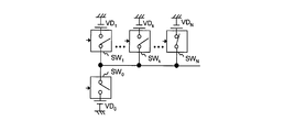
- FIG. 2 shows a general configuration example of a multi-level class D amplifier with multi-level output voltage.
- the multilevel class D amplifier shown in FIG. 2 includes a plurality (N + 1) of switch elements SW 0 , SW 1 ,... Connected between a plurality (N + 1) of power supplies and output terminals. , SW N.
- the plurality of switch elements SW 0 , SW 1 ,..., SW N are controlled such that only one of the switch elements is turned on.
- the output voltage is the power supply voltage of the power supply connected to the switch element in the ON state. That is, the multi-level class D amplifier can output the same number of voltage values as the number of power supplies.
- a digital baseband (hereinafter referred to as DBB) signal is generated and amplified.
- DBB signal is a multi-bit signal of 10 bits or more, while the number of bits that can be input to the class D amplifier is generally smaller than the number of bits of the DBB signal.
- the delta-sigma modulator is a circuit technology that can reduce the number of bits while avoiding an increase in quantization noise in a band near a desired frequency.
- a DBB signal or an amplitude signal generated based on the DBB signal is delta-sigma modulated by the delta-sigma modulator.
- the number of bits of the output signal of the delta-sigma modulator is set equal to the number of bits that can be input to the class D amplifier provided in the subsequent stage.
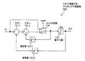
- FIG. 3 shows a typical configuration example of a delta-sigma modulator (p. 71 of Non-Patent Document 1).
- the delta sigma modulator shown in FIG. 3 includes adders 131-1, 131-2, delay units 132-1, 132-2, and a quantizer 300. Note that the delay unit 132-1 and the adder 131-2 constitute an internal integrator.
- the quantizer 300 quantizes the output signal of the adder 131-2 with a predetermined number of bits.
- Delay device 132-2 delays the output signal of quantizer 300 by 1 clock.
- the adder 131-1 calculates the difference between the input signal and the output signal of the delay unit 132-2.
- Delay device 132-1 delays the output signal of adder 131-2 by 1 clock.
- the adder 131-2 calculates the sum of the output signal of the adder 131-1 and the output signal of the delay unit 132-1.
- Noise N (z) included in the output signal V (z) is expressed by the following equation.
- f is the signal frequency of the radio signal
- fclk is the clock frequency of the delta-sigma modulator
- the integrated noise in the signal band is expressed by the following equation.
- an SNR Signal-Noise Ratio
- an SNR Signal-Noise Ratio in the vicinity of a desired signal band is required to be 33 dB or more.
- Non-Patent Document 2 reports a delta-sigma modulator operating at 4 GHz fclk. In order to keep E (z) small, it is necessary to make the quantizer 300 multi-bit. In Non-Patent Document 2, 1 bit is adopted as the number of bits of the quantizer. However, in the method reported in Non-Patent Document 2, when the number of bits of the quantizer is increased, the operation speed, that is, fclk is increased. descend.
- the related transmitter has a problem that it is impossible to achieve both high-speed operation and reduction of quantization noise in the delta-sigma modulator.
- An object of the present invention is to provide a transmitter and a transmission method capable of solving the above-described problems and achieving both high-speed operation and reduction of quantization noise in a delta-sigma modulator.
- the transmitter of the present invention is A level detector for detecting which level value the input signal corresponds to among a predetermined number of level values; For the input signal, a pre-stage signal conditioner that performs amplification and offset amount shift according to the output signal of the level detector; A delta-sigma modulator comprising a quantizer that performs quantization with a predetermined number of bits on the output signal of the preceding signal conditioner; A post-stage signal adjuster that performs amplification and offset amount shifting on the output signal of the delta-sigma modulator in accordance with the output signal of the level detector.
- the transmission method of the present invention includes: A transmission method by a transmitter, Detects which level value the input signal corresponds to among a predetermined number of level values, For the input signal, according to the level value of the input signal, as a pre-stage signal processing, amplification and offset amount shift, The signal subjected to the preceding signal processing is quantized with a predetermined number of bits, A transmission method for performing amplification and shifting an offset amount as post-stage signal processing on the quantized signal in accordance with a level value of the input signal.
- the transmitter of the present invention since the signal is amplified by the preceding signal conditioner before being subjected to the delta sigma modulation by the delta sigma modulator, the signal power with respect to the quantization noise generated when the delta sigma modulation is performed. A large ratio can be taken. Therefore, the quantization noise for the signal strength is relatively reduced. Further, as the delta sigma modulator, a delta sigma modulator having a 1-bit quantizer can be used, and high-speed operation can be ensured.
- FIG. 5 is a circuit block diagram illustrating a configuration example of the delta-sigma modulator illustrated in FIG. 4.
- FIG. 5 is a circuit block diagram illustrating a configuration example of a post-level adjuster illustrated in FIG. 4. It is a circuit block diagram which shows the structural example of the transmitting apparatus of the 2nd Embodiment of this invention.
- FIG. 8 is a circuit block diagram illustrating a configuration example of the delta sigma modulator with a reset function illustrated in FIG. 7.
- FIG. 8 is a circuit block diagram illustrating a configuration example of the level transition detector illustrated in FIG. 7.
- FIG. 8 is a circuit block diagram illustrating a configuration example of the delta sigma modulator with a reset function illustrated in FIG. 7.
- FIG. 8 is a circuit block diagram illustrating a configuration example of the delta sigma modulator with a reset function illustrated in FIG. 7.
- It is a circuit block diagram which shows the structural example of the transmitting apparatus of the 3rd Embodiment of this invention.
- It is a circuit block diagram which shows the structural example of the pulse phase signal generator shown in FIG.
- It is a circuit block diagram which shows the application example of the transmitter of the 2nd Embodiment of this invention.
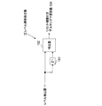
- FIG. 4 shows a configuration example around a delta-sigma modulator of a transmitter according to a first embodiment of the present invention.
- the transmitter of the present embodiment includes a level detector 11, a pre-level adjuster 12 that is a front-stage signal conditioner, a delta-sigma modulator 13, and a post-level adjuster 14 that is a subsequent-stage signal conditioner. And have.
- the circuit including the components shown in FIG. 4 will be referred to as a “digital modulator”.
- the level detector 11 detects which level value the input signal corresponds to among a predetermined number of level values.
- the value of the input signal assigned to each level value is as follows.
- the input possible range of the level detector 11 is V MIN to V MAX .
- Level value 1 V MIN to V 1
- Level value 2 V 1 to V 2
- Level value N V N-1 to V MAX
- the pre-level adjuster 12 performs amplification and offset amount shift (that is, potential shift) on the input signal according to the level value detected by the level detector 11, and a delta-sigma modulator 13 provided in the subsequent stage. Match with the input range of.
- the level value detected by the level detector 11 is k (that is, the value of the input signal is V k-1 to V k ), and the pre-level
- the transfer function of the regulator 12 is expressed by the following equation.
- the input signal of the pre-level adjuster 12 is Vtunein
- the output signal is Vtuneout.
- the above transfer function corresponds to a linear transformation in which the output signal is Vdsmmin when the input signal is V k ⁇ 1 and the output signal is Vdsmmax when the input signal is V k .
- the delta sigma modulator 13 is composed of a first order delta sigma modulator in which the quantizer 300 shown in FIG. 3 is replaced with a 1-bit quantizer 133.
- the output signal of the delta-sigma modulator 13 is a high / low 1-bit signal, the output value that is actually assigned to high as a physical quantity is Vdsmmax, and the output value that is assigned to low as a physical quantity is Vdsmmin.
- the output value assigned to the output signal high / low of the delta-sigma modulator 13 can take a value other than Vdsmmax / Vdsmmin.
- delta sigma modulator 13 is not limited to the configuration of FIG. 5, and may be a delta sigma modulator having quantizers of different orders and different numbers of bits and having different transfer functions.
- the post-level adjuster 14 performs amplification and shift of the offset amount on the output signal of the delta-sigma modulator 13 using the inverse function of the transfer function of the pre-level adjuster 12.
- the post-level adjuster 14 amplifies the output signal of the delta-sigma modulator 13 with an amplification factor that is the reciprocal of the amplification factor that is performed by the pre-level adjuster 12, and the offset amount that is performed by the pre-level adjuster 12.
- the offset amount is shifted by the same amount in the opposite direction to the shift (that is, the potential shift is performed by the same amount in the opposite direction to the potential shift performed by the pre-level adjuster 12).
- the above transfer function corresponds to a linear transformation in which the output signal is V k-1 when the input signal is Vdsmmin, and the output signal is V k when the input signal is Vdsmmax.
- the output signal V (z) of the delta-sigma modulator 13 is obtained as follows by substituting the right side of Expression (7) into U (z) of Expression (1).
- the output signal Vpostout of the post level adjuster 14 can be obtained as follows by substituting the right side of the equation (8) into Vpostin of the equation (6).
- Equation (9) includes an input signal and a quantization noise term.
- the minimum / maximum value (V MIN / V MAX ) of the input range of the level detector 11 is the minimum / maximum value (Vdsmmax / Vdsmin) of the input range of the delta-sigma modulator 13.
- the step size of the level value in the level detector 11 is constant at 1/8 of the input possible range of the delta-sigma modulator 13.
- the coefficient of quantization noise in Equation (9) is 1/8.
- a 1-bit quantizer 133 was adopted, while a 4-bit quantizer was adopted. Reduction to quantization noise corresponding to the case can be realized.
- the input signal input to the digital modulator is amplified before being input to the internal delta-sigma modulator 13 (in equation (5),
- the coefficient “Vdsmax ⁇ Vdsmin / (V k ⁇ V k ⁇ 1 )” applied to the term including Vtunein corresponds to the amplification factor). Therefore, the quantization noise is relatively reduced and the SNR is improved.
- FIG. 6 shows a configuration example of the post-level adjuster 14.
- the post-level adjuster 14 includes a decoder 141, driver amplifiers 142 0 , 142 1 ,..., 142 N, and a multi-value class D amplifier 143.
- the multi-value class D amplifier 143 is the same as the multi-value class D amplifier shown in FIG.
- Decoder 141 based on the output signal of the output signal and the level detector 11 of the delta-sigma modulator 13, driver amplifier 142 0, 142 1, ..., through 142 N, the switch element SW 0, SW 1, ..., and outputs a switching control signal to SW N, performs switching element SW 0, SW 1, ..., the opening and closing control of the SW N.
- the multi-level class-D amplifier 143 includes N + 1 switch elements SW 0 , SW 1 ,..., SW N connected to N + 1 power sources.
- the power supply voltage values VD 0 , VD 1 ,..., VD N of N + 1 power supplies are the boundary values V MIN , V 1 , V 2 ,. , V N-1 , V MAX are related as follows:
- a and b are arbitrary constants.
- the decoder 141 Based on the output signal of the level detector 11 and the output signal of the delta-sigma modulator 13, the decoder 141 switches each of the switch elements SW 0 , SW 1 ,. SW N Open / Close control signal is generated.
- the decoder 141 if the detected level at the level detector 11 is k, the switch element SW k if 1bit signal outputted from the delta sigma modulator 13 is a high, switching elements it is low SW k -1 is turned on. Note that only one switch element is in the ON state, and the other switch elements are in the OFF state.
- the output voltage of the multi-level class D amplifier 143 becomes VD k if the 1-bit signal output from the delta-sigma modulator 13 is high, and VD k-1 if it is low.
- the output signal of the multilevel D-class amplifier 143 is expressed by the following equation.
- Equation (13) corresponds to the fact that the coefficient a is applied to the right side of Equation (9) and b is added as the offset amount shift amount (ie, potential shift amount).
- FIG. 7 shows a configuration example around a delta-sigma modulator of a transmitter according to a second embodiment of the present invention.
- the transmitter of the present embodiment is different from the first embodiment of FIG. 4 in that the delta sigma modulator 13 is replaced with a delta sigma modulator 13A with a reset function, and with a reset function.
- the difference is that a level transition detector 15 for generating a reset signal reset to be supplied to the delta-sigma modulator 13A is added.
- the circuit including the components shown in FIG. 7 is referred to as a “digital modulator”.
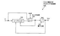
- FIG. 8 shows a configuration example of the delta-sigma modulator 13A with a reset function.
- the delta sigma modulator 13A with a reset function is different from the delta sigma modulator 13 shown in FIG. 5 in that a selector circuit 134 is inserted after the adder 131-2.
- the selector circuit 134 In response to the reset signal reset input from the level transition detector 15, the selector circuit 134 converts the input signal of the quantizer 133 and the delay device 132-1 into the output signal of the adder 131-2 or delta-sigma modulation with a reset function. Switch to one of the input signals of the device 13A.
- the reset signal reset when the reset signal reset is high, the input signal is switched to the input signal of the delta sigma modulator 13A with a reset function.
- FIG. 9 shows a configuration example of the level transition detector 15.
- the level transition detector 15 includes a delay unit 151 and a determination unit 152.
- the delay device 151 delays the input signal of the level transition detector 15 by 1 clock.
- the determiner 152 compares the input signal of the level transition detector 15 and the input signal of 1 clock before (that is, the output signal of the delay device 151) to determine whether or not they are equal. If they are not equal, high is output as the reset signal reset.
- the input signal of the level transition detector 15 is the output signal of the level detector 11.
- the delta sigma modulator 13A with a reset function has the same configuration as the delta sigma modulator 13 shown in FIG.
- the input signal of the delta sigma modulator 13A with a reset function is directly input to the quantizer 133 and the delay unit 132-1 in the delta sigma modulator 13A with a reset function.
- the input signal of the delay unit 132-1 is forced to become the input signal of the delta-sigma modulator 13A with reset function, and an internal integrator composed of the delay unit 132-1 and the adder 131-2. Is reset. That is, the input signal of the quantizer 133 is the input signal of the delta sigma modulator 13A with a reset function without depending on the level state of 1 clock before.
- the input signal of the quantizer 133 is the sum of the output signal of the adder 131-1 and the input signal of the delay unit 132-1 before 1 clock. It is affected by the level status of 1 clock before.
- the internal integrator of the delta-sigma modulator 13A with a reset function is reset.
- the delta sigma modulator 13A with a reset function can perform the delta sigma modulation without depending on the level state of the input signal one clock before.
- Other effects are the same as those of the first embodiment.
- FIGS. 10 and 11 show other configuration examples of the delta-sigma modulator 13A with a reset function.
- the quantizer 133 is the same as that shown in FIG.
- the selector circuit 134 is inserted into the output section of the loop filter 135.
- FIG. 8 shows an example in which the loop filter 135 is configured by an adder 131-1, an adder 131-2, a delay unit 132-1, and a delay unit 132-2 to realize a first-order delta-sigma modulator.
- the loop filter 135 is not limited to the configuration of FIG. 8 and may be configured to realize a high-order delta-sigma modulator.
- the configuration of the loop filter 135 that realizes a second-order delta-sigma modulator is disclosed in p.64 of Non-Patent Document 1.
- FIG. 11 differs from FIG. 8 in that the selector circuit 134 is replaced with a selector circuit 136 inserted in front of the delay unit 131-1 as compared with the delta sigma modulator 13A with reset function shown in FIG.
- the selector circuit 136 converts the input signal of the delay unit 132-1 into the output signal of the adder 131-2 or the input signal of the delta sigma modulator 13A with a reset function in accordance with the reset signal reset input from the level transition detector 15. Switch to one of the following.
- FIG. 12 shows a configuration example of the entire transmitter according to the third embodiment of the present invention.
- the transmitter includes a level detector 11, a pre-level adjuster 12 that is a pre-stage signal adjuster, a delta-sigma modulator 13, and a post-level adjuster 14 that is a post-stage signal adjuster.
- a digital baseband signal generation unit 16 an IQ modulator 17, a pulse phase signal generator 18, a multiplier 19, a filter element 20, and an antenna 21.
- the digital baseband signal generator 16 generates quadrature baseband signals I (t) and Q (t) and an amplitude signal A (t).
- the amplitude signal A (t) is equal to the square root of the square sum of the quadrature baseband signals I (t) and Q (t).
- the IQ modulator 17 generates the RF signal RF (t) based on the quadrature baseband signals I (t) and Q (t) according to the following equation.
- Equation (14) is rewritten into the following equation using the amplitude signal A (t) and the phase signal ⁇ (t).
- ⁇ is an angular frequency given by multiplying the carrier frequency by 2 ⁇ .
- the RF phase signal RF ⁇ (t) is defined by the following equation.
- the IQ modulator 17 inputs the RF phase signal RF ⁇ (t) to the pulse phase signal generator 18.
- FIG. 13 shows a configuration example of the pulse phase signal generator 18.
- the pulse phase signal generator 18 has a comparator 181 and a phase signal level adjuster 182.
- the RF phase signal RF ⁇ (t) is compared with a zero value in the comparator 181 and converted into a rectangular phase signal RF ⁇ rec (t) to which 1 is assigned if greater than zero and -1 is assigned if less.
- Dis (t) corresponds to the harmonic component of RF ⁇ (t).
- RF ⁇ rec (t) takes a value of ⁇ 1 or 1.
- phase adjustment of the rectangular phase signal RF ⁇ rec (t) is performed by the phase signal level adjuster 182 as shown in the following expression, and converted into the pulse phase signal RF ⁇ pul (t).
- the pulse phase signal RF ⁇ pul (t) takes a value of 0 or 1.
- the pulse phase signal RF ⁇ pul (t) is used as a signal to be input to the logic circuit, for example, as a clock signal for the delta sigma modulator 13, 0 is assigned to low and 1 is assigned to high.
- connection relationship between the level detector 11, the pre-level adjuster 12, the delta sigma modulator 13, and the post level adjuster 14 is a multiplier between the delta sigma modulator 13 and the post level adjuster 14. Except that 19 is inserted, it is the same as the first embodiment.
- the configurations of the level detector 11, the pre-level adjuster 12, and the delta-sigma modulator 13 are the same as those in the first embodiment.
- the post-level adjuster 14 is different from the configuration of FIG. 6 in that the multi-value class D amplifier 143 is replaced with a multi-value class D amplifier 143A to which the switch element SW p is added, and accordingly, a driver amplifier. 142 p is different from that added.
- the amplitude signal A (t) output from the digital baseband signal generation unit 16 is an input signal of the digital modulator described in the first embodiment.
- the pulse phase signal RF ⁇ pul (t) output from the pulse phase signal generator 18 is input to the multiplier 19 and also input to the delta sigma modulator 13 as a clock signal for driving the delta sigma modulator 13.
- the components in the delta-sigma modulator 13 perform the above-described operation using the pulse phase signal RF ⁇ pul (t) as a clock signal. With this configuration, the two pulse signals (the output signal of the delta sigma modulator 13 and the output signal of the pulse phase signal generator 18) input to the multiplier 19 are synchronized.
- the multiplier 19 integrates the output signal of the delta-sigma modulator 13 and the pulse phase signal RF ⁇ pul (t) to generate a digital signal containing a desired RF signal.
- the output signal of the multiplier 19 is the output signal itself of the delta-sigma modulator 13 when the value of the pulse phase signal RF ⁇ pul (t) is 1, and when the value of the pulse phase signal RF ⁇ pul (t) is 0, 0.
- the multi-level class-D amplifier 143A includes N + 2 switch elements SW p , SW 0 , SW 1 ,..., SW N connected to N + 2 power sources, respectively. .
- the power supply voltage values Vp, VD 0 , VD 1 ,..., VD N ) of N + 2 power supplies are the boundary values V MIN , V 1 , V 2 , .., V N-1 , V MAX are associated with the following equations.
- the decoder 141 performs the switching elements SW p , SW 0 , SW 1 ,... Of the multilevel D-class amplifier 143A based on the output signal of the level detector 11 and the output signal of the multiplier 19 as follows. , SW N open / close control signal is generated.
- the decoder 141 when the output signal of the multiplier 19 is zero, i.e., when the value of the pulse phase signal RF ⁇ pul (t) is 0, the switch element SW p in ON state.
- the output signal of the multiplier 19 is not 0, that is, when the value of the pulse phase signal RF ⁇ pul (t) is 1, the output signal of the multiplier 19 is the output signal of the delta-sigma modulator 13 itself.
- the decoder 141 switches the switch element SW if the 1-bit signal output from the delta-sigma modulator 13 is high. If k is low, the switch element SW k-1 is turned on. Note that only one switch element is in the ON state, and the other switch elements are in the OFF state.
- the output signal of the multi-level class D amplifier 143A is b when the value of the pulse phase signal RF ⁇ pul (t) is 0, and when it is 1, the output signal is shown in the equation (13).
- the output signal of the multilevel D-class amplifier 134 in the first embodiment a value obtained by substituting the Z-converted amplitude signal (A (t) in the time domain) into S (z) on the left side.
- the output signal VDout2 (t) of the multilevel D-class amplifier 143A is given as follows.
- Expression (23) corresponds to an expression rewritten in the time domain after substituting the Z-transformed amplitude signal (A (t) in the time domain) into S (z) in Expression (13).
- Edsm (t) is quantization noise generated in the delta-sigma modulator 13, and becomes (1-z -1 E (z)) after Z conversion.
- a (t) ⁇ RF ⁇ (t)” in the curly brackets in the first term on the right side of Equation (25) is the RF signal RF (t) with reference to Equation (15) and Equation (18).
- the quantization noise Edsm (t) is multiplied by a coefficient V k ⁇ V k ⁇ 1 of the level value detected by the level detector 11.
- V k ⁇ V k ⁇ 1 is a range of level values detected by the level detector 11. Therefore, the smaller this range, the smaller the proportion of quantization noise in VDout2 (t).
- the output signal VDout2 (t) of the multi-level class D amplifier 143A is radiated from the antenna 21 into the air after the filter element 20 has sufficiently suppressed frequency components other than the desired frequency component. Note that the second and subsequent terms on the right side of Equation (25) are out-of-band components and are suppressed by the filter element 20.
- this embodiment corresponds to the case where a delta sigma modulator having a multi-bit quantizer is adopted while realizing a high speed operation by adopting a delta sigma modulator 13 having a 1-bit quantizer 133.
- the effect that it can reduce to the quantization noise which carries out is acquired.
- the configuration using the delta sigma modulator 13 of the first embodiment has been described.
- the delta sigma modulator 13A with a reset function and the level of the second embodiment are provided.
- a configuration using the transition detector 15 may be adopted.
- the internal integrator when the level value of the input signal changes, the internal integrator is reset and delta-sigma modulation is performed without depending on the previous level state.
- the internal integrator when the input signal becomes discontinuous, the internal integrator may be reset and applied to a configuration in which delta-sigma modulation is performed without depending on the previous level state.
- the internal integrator of the delta-sigma modulator 13A with a reset function may be reset.
- the discontinuity of the input signal can be detected using, for example, a baseband signal.
- the configuration of FIG. 8 is used as the delta-sigma modulator 13A with a reset function, but the configuration of FIG. 10 or FIG. 11 may be used.
Landscapes
- Engineering & Computer Science (AREA)
- Power Engineering (AREA)
- Theoretical Computer Science (AREA)
- Computer Networks & Wireless Communication (AREA)
- Signal Processing (AREA)
- Compression, Expansion, Code Conversion, And Decoders (AREA)
- Amplifiers (AREA)
Priority Applications (2)
| Application Number | Priority Date | Filing Date | Title |
|---|---|---|---|
| US14/380,849 US9160379B2 (en) | 2012-03-22 | 2013-02-19 | Transmitter and transmitting method |
| JP2014506085A JP6164208B2 (ja) | 2012-03-22 | 2013-02-19 | 送信機および送信方法 |
Applications Claiming Priority (2)
| Application Number | Priority Date | Filing Date | Title |
|---|---|---|---|
| JP2012066261 | 2012-03-22 | ||
| JP2012-066261 | 2012-03-22 |
Publications (1)
| Publication Number | Publication Date |
|---|---|
| WO2013140914A1 true WO2013140914A1 (fr) | 2013-09-26 |
Family
ID=49222379
Family Applications (1)
| Application Number | Title | Priority Date | Filing Date |
|---|---|---|---|
| PCT/JP2013/053908 Ceased WO2013140914A1 (fr) | 2012-03-22 | 2013-02-19 | Émetteur et procédé de transmission |
Country Status (3)
| Country | Link |
|---|---|
| US (1) | US9160379B2 (fr) |
| JP (1) | JP6164208B2 (fr) |
| WO (1) | WO2013140914A1 (fr) |
Cited By (2)
| Publication number | Priority date | Publication date | Assignee | Title |
|---|---|---|---|---|
| JP2017521886A (ja) * | 2014-05-05 | 2017-08-03 | アルカテル−ルーセント | 無線周波数通信のための信号変調 |
| JP2018074303A (ja) * | 2016-10-27 | 2018-05-10 | 日本電気株式会社 | 送受信機および送受信機の制御方法 |
Families Citing this family (1)
| Publication number | Priority date | Publication date | Assignee | Title |
|---|---|---|---|---|
| DE102024209718A1 (de) | 2024-10-04 | 2026-04-09 | Robert Bosch Gesellschaft mit beschränkter Haftung | Analog-Digital-Umsetzer und Verfahren zum Betreiben eines Analog-Digital-Umsetzers |
Citations (3)
| Publication number | Priority date | Publication date | Assignee | Title |
|---|---|---|---|---|
| JPS647437U (fr) * | 1987-07-03 | 1989-01-17 | ||
| JPH07254823A (ja) * | 1994-03-14 | 1995-10-03 | Kenwood Corp | デルタシグマ変調増幅器 |
| JP2000049613A (ja) * | 1998-07-31 | 2000-02-18 | Sharp Corp | ディジタルスイッチングアンプ |
Family Cites Families (18)
| Publication number | Priority date | Publication date | Assignee | Title |
|---|---|---|---|---|
| JPS5394813A (en) * | 1977-01-31 | 1978-08-19 | Toshiba Corp | Signal process system |
| JPH077426A (ja) * | 1993-06-18 | 1995-01-10 | Nec Corp | A/d変換装置 |
| JPH07212234A (ja) | 1994-01-25 | 1995-08-11 | Hitachi Ltd | Da変換器およびそれを用いた周波数シンセサイザ |
| US6917241B2 (en) * | 2002-05-13 | 2005-07-12 | Matsushita Electric Industrial Co., Ltd. | Amplifier circuit, transmission device, amplification method, and transmission method |
| US6639539B1 (en) * | 2002-10-22 | 2003-10-28 | Bei Technologies, Inc. | System and method for extending the dynamic range of an analog-to-digital converter |
| JP2004165905A (ja) | 2002-11-12 | 2004-06-10 | Hitachi Ulsi Systems Co Ltd | 半導体集積回路 |
| JP4122325B2 (ja) * | 2004-10-01 | 2008-07-23 | 松下電器産業株式会社 | 利得制御機能付きデルタシグマ変調回路 |
| JP4829695B2 (ja) | 2006-06-16 | 2011-12-07 | パナソニック株式会社 | A/d変換器 |
| KR101079813B1 (ko) * | 2007-10-02 | 2011-11-04 | 삼성전자주식회사 | 무선통신 시스템에서 전력증폭 장치 및 방법 |
| JP4470995B2 (ja) * | 2007-12-19 | 2010-06-02 | セイコーエプソン株式会社 | A/d変換回路及び電子機器 |
| JP4497213B2 (ja) * | 2008-02-21 | 2010-07-07 | セイコーエプソン株式会社 | 集積回路装置及び電子機器 |
| JP2011066626A (ja) | 2009-09-16 | 2011-03-31 | Asahi Kasei Electronics Co Ltd | A/d変換装置、icチップ |
| EP2518901B1 (fr) * | 2009-12-21 | 2016-03-30 | Nec Corporation | Circuit de génération de signaux rf et émetteur sans fil |
| EP2367076B1 (fr) | 2010-03-17 | 2018-08-08 | Glashütter Uhrenbetrieb GmbH | Dispositif d'alarme réglable 30 jours à l'avance |
| JP5032637B2 (ja) * | 2010-07-30 | 2012-09-26 | 株式会社東芝 | 増幅器及びそれを用いた無線送信機 |
| JP5725027B2 (ja) * | 2010-08-03 | 2015-05-27 | 日本電気株式会社 | 送信装置及びその制御方法 |
| KR20120071504A (ko) * | 2010-12-23 | 2012-07-03 | 한국전자통신연구원 | 증폭 구조 및 그것의 증폭 방법 |
| KR20120118340A (ko) * | 2011-04-18 | 2012-10-26 | 한국전자통신연구원 | 신호 증폭장치, 무선 송신장치 및 그 방법 |
-
2013
- 2013-02-19 US US14/380,849 patent/US9160379B2/en active Active
- 2013-02-19 WO PCT/JP2013/053908 patent/WO2013140914A1/fr not_active Ceased
- 2013-02-19 JP JP2014506085A patent/JP6164208B2/ja active Active
Patent Citations (3)
| Publication number | Priority date | Publication date | Assignee | Title |
|---|---|---|---|---|
| JPS647437U (fr) * | 1987-07-03 | 1989-01-17 | ||
| JPH07254823A (ja) * | 1994-03-14 | 1995-10-03 | Kenwood Corp | デルタシグマ変調増幅器 |
| JP2000049613A (ja) * | 1998-07-31 | 2000-02-18 | Sharp Corp | ディジタルスイッチングアンプ |
Cited By (2)
| Publication number | Priority date | Publication date | Assignee | Title |
|---|---|---|---|---|
| JP2017521886A (ja) * | 2014-05-05 | 2017-08-03 | アルカテル−ルーセント | 無線周波数通信のための信号変調 |
| JP2018074303A (ja) * | 2016-10-27 | 2018-05-10 | 日本電気株式会社 | 送受信機および送受信機の制御方法 |
Also Published As
| Publication number | Publication date |
|---|---|
| JPWO2013140914A1 (ja) | 2015-08-03 |
| US9160379B2 (en) | 2015-10-13 |
| US20150049842A1 (en) | 2015-02-19 |
| JP6164208B2 (ja) | 2017-07-19 |
Similar Documents
| Publication | Publication Date | Title |
|---|---|---|
| CN1792038B (zh) | ∑-δ调制器和∑-δ调制方法 | |
| EP3229371B1 (fr) | Système d'amplificateur audio | |
| US9240801B2 (en) | Analog-to-digital converter | |
| US9991904B2 (en) | Digital modulation device, and digital modulation method | |
| KR20140011135A (ko) | 오프셋 전압 보정 장치 및 방법과 이를 포함한 연속 시간 델타 시그마 변조 장치 | |
| KR101696269B1 (ko) | 델타-시그마 변조기 및 이를 포함하는 송신장치 | |
| US20100329482A1 (en) | Audio digital to analog converter and audio processing apparatus including the same | |
| CN108696281B (zh) | 功率缩放连续时间δ-σ调制器 | |
| US9071303B2 (en) | Level de-multiplexed delta sigma modulator based transmitter | |
| US8681029B1 (en) | Chopper-stabilization method and apparatus for sigma delta modulators | |
| JP6032203B2 (ja) | Rf信号生成回路、及び送信機 | |
| US8299866B2 (en) | Method and device including signal processing for pulse width modulation | |
| US9166617B1 (en) | Communication unit, digital band-pass sigma-delta modulator and method therefor | |
| JP6164208B2 (ja) | 送信機および送信方法 | |
| US9985645B2 (en) | Techniques for improving mismatch shaping of dynamic element matching circuit within delta-sigma modulator | |
| JP5892162B2 (ja) | デジタル変調器 | |
| US8526638B2 (en) | Gain control circuit and electronic volume circuit | |
| WO2000070752A1 (fr) | Amplificateur numerique | |
| JP6801791B2 (ja) | Rf信号生成装置およびrf信号生成方法 | |
| Majd et al. | Bandwidth enhancement in delta sigma modulator transmitter using low complexity time-interleaved parallel delta sigma modulator | |
| Singh et al. | Performance analysis of multilevel delta sigma modulators for 3G/4G communication | |
| JPWO2020175581A1 (ja) | デルタシグマ変調装置及び通信機器 | |
| Adrian et al. | A review of design methods for digital modulators | |
| JP7006214B2 (ja) | 信号生成装置、及び信号生成方法 | |
| KR20090061134A (ko) | 데이터 가중 평균화 알고리즘을 이용하는 디급 오디오증폭기 |
Legal Events
| Date | Code | Title | Description |
|---|---|---|---|
| 121 | Ep: the epo has been informed by wipo that ep was designated in this application |
Ref document number: 13764987 Country of ref document: EP Kind code of ref document: A1 |
|
| WWE | Wipo information: entry into national phase |
Ref document number: 14380849 Country of ref document: US |
|
| ENP | Entry into the national phase |
Ref document number: 2014506085 Country of ref document: JP Kind code of ref document: A |
|
| NENP | Non-entry into the national phase |
Ref country code: DE |
|
| 122 | Ep: pct application non-entry in european phase |
Ref document number: 13764987 Country of ref document: EP Kind code of ref document: A1 |