WO2013141268A1 - Substrat avec film réfléchissant multicouche, ébauche de masque réfléchissant pour la lithographie euv, procédé de production d'une ébauche réfléchissante pour la lithographie euv, et procédé de fabrication d'un dispositif à semi-conducteur - Google Patents
Substrat avec film réfléchissant multicouche, ébauche de masque réfléchissant pour la lithographie euv, procédé de production d'une ébauche réfléchissante pour la lithographie euv, et procédé de fabrication d'un dispositif à semi-conducteur Download PDFInfo
- Publication number
- WO2013141268A1 WO2013141268A1 PCT/JP2013/057957 JP2013057957W WO2013141268A1 WO 2013141268 A1 WO2013141268 A1 WO 2013141268A1 JP 2013057957 W JP2013057957 W JP 2013057957W WO 2013141268 A1 WO2013141268 A1 WO 2013141268A1
- Authority
- WO
- WIPO (PCT)
- Prior art keywords
- film
- substrate
- alloy
- multilayer reflective
- reflective film
- Prior art date
- Legal status (The legal status is an assumption and is not a legal conclusion. Google has not performed a legal analysis and makes no representation as to the accuracy of the status listed.)
- Ceased
Links
Images



Classifications
-
- H—ELECTRICITY
- H10—SEMICONDUCTOR DEVICES; ELECTRIC SOLID-STATE DEVICES NOT OTHERWISE PROVIDED FOR
- H10P—GENERIC PROCESSES OR APPARATUS FOR THE MANUFACTURE OR TREATMENT OF DEVICES COVERED BY CLASS H10
- H10P76/00—Manufacture or treatment of masks on semiconductor bodies, e.g. by lithography or photolithography
- H10P76/20—Manufacture or treatment of masks on semiconductor bodies, e.g. by lithography or photolithography of masks comprising organic materials
- H10P76/204—Manufacture or treatment of masks on semiconductor bodies, e.g. by lithography or photolithography of masks comprising organic materials of organic photoresist masks
- H10P76/2041—Photolithographic processes
-
- G—PHYSICS
- G03—PHOTOGRAPHY; CINEMATOGRAPHY; ANALOGOUS TECHNIQUES USING WAVES OTHER THAN OPTICAL WAVES; ELECTROGRAPHY; HOLOGRAPHY
- G03F—PHOTOMECHANICAL PRODUCTION OF TEXTURED OR PATTERNED SURFACES, e.g. FOR PRINTING, FOR PROCESSING OF SEMICONDUCTOR DEVICES; MATERIALS THEREFOR; ORIGINALS THEREFOR; APPARATUS SPECIALLY ADAPTED THEREFOR
- G03F1/00—Originals for photomechanical production of textured or patterned surfaces, e.g., masks, photo-masks, reticles; Mask blanks or pellicles therefor; Containers specially adapted therefor; Preparation thereof
- G03F1/22—Masks or mask blanks for imaging by radiation of 100nm or shorter wavelength, e.g. X-ray masks, extreme ultraviolet [EUV] masks; Preparation thereof
- G03F1/24—Reflection masks; Preparation thereof
-
- B—PERFORMING OPERATIONS; TRANSPORTING
- B82—NANOTECHNOLOGY
- B82Y—SPECIFIC USES OR APPLICATIONS OF NANOSTRUCTURES; MEASUREMENT OR ANALYSIS OF NANOSTRUCTURES; MANUFACTURE OR TREATMENT OF NANOSTRUCTURES
- B82Y10/00—Nanotechnology for information processing, storage or transmission, e.g. quantum computing or single electron logic
-
- B—PERFORMING OPERATIONS; TRANSPORTING
- B82—NANOTECHNOLOGY
- B82Y—SPECIFIC USES OR APPLICATIONS OF NANOSTRUCTURES; MEASUREMENT OR ANALYSIS OF NANOSTRUCTURES; MANUFACTURE OR TREATMENT OF NANOSTRUCTURES
- B82Y40/00—Manufacture or treatment of nanostructures
-
- G—PHYSICS
- G03—PHOTOGRAPHY; CINEMATOGRAPHY; ANALOGOUS TECHNIQUES USING WAVES OTHER THAN OPTICAL WAVES; ELECTROGRAPHY; HOLOGRAPHY
- G03F—PHOTOMECHANICAL PRODUCTION OF TEXTURED OR PATTERNED SURFACES, e.g. FOR PRINTING, FOR PROCESSING OF SEMICONDUCTOR DEVICES; MATERIALS THEREFOR; ORIGINALS THEREFOR; APPARATUS SPECIALLY ADAPTED THEREFOR
- G03F1/00—Originals for photomechanical production of textured or patterned surfaces, e.g., masks, photo-masks, reticles; Mask blanks or pellicles therefor; Containers specially adapted therefor; Preparation thereof
- G03F1/38—Masks having auxiliary features, e.g. special coatings or marks for alignment or testing; Preparation thereof
- G03F1/48—Protective coatings
-
- H—ELECTRICITY
- H10—SEMICONDUCTOR DEVICES; ELECTRIC SOLID-STATE DEVICES NOT OTHERWISE PROVIDED FOR
- H10P—GENERIC PROCESSES OR APPARATUS FOR THE MANUFACTURE OR TREATMENT OF DEVICES COVERED BY CLASS H10
- H10P76/00—Manufacture or treatment of masks on semiconductor bodies, e.g. by lithography or photolithography
- H10P76/40—Manufacture or treatment of masks on semiconductor bodies, e.g. by lithography or photolithography of masks comprising inorganic materials
- H10P76/405—Manufacture or treatment of masks on semiconductor bodies, e.g. by lithography or photolithography of masks comprising inorganic materials characterised by their composition, e.g. multilayer masks
-
- H—ELECTRICITY
- H10—SEMICONDUCTOR DEVICES; ELECTRIC SOLID-STATE DEVICES NOT OTHERWISE PROVIDED FOR
- H10P—GENERIC PROCESSES OR APPARATUS FOR THE MANUFACTURE OR TREATMENT OF DEVICES COVERED BY CLASS H10
- H10P76/00—Manufacture or treatment of masks on semiconductor bodies, e.g. by lithography or photolithography
- H10P76/40—Manufacture or treatment of masks on semiconductor bodies, e.g. by lithography or photolithography of masks comprising inorganic materials
- H10P76/408—Manufacture or treatment of masks on semiconductor bodies, e.g. by lithography or photolithography of masks comprising inorganic materials characterised by their sizes, orientations, dispositions, behaviours or shapes
- H10P76/4085—Manufacture or treatment of masks on semiconductor bodies, e.g. by lithography or photolithography of masks comprising inorganic materials characterised by their sizes, orientations, dispositions, behaviours or shapes characterised by the processes involved to create the masks
-
- Y—GENERAL TAGGING OF NEW TECHNOLOGICAL DEVELOPMENTS; GENERAL TAGGING OF CROSS-SECTIONAL TECHNOLOGIES SPANNING OVER SEVERAL SECTIONS OF THE IPC; TECHNICAL SUBJECTS COVERED BY FORMER USPC CROSS-REFERENCE ART COLLECTIONS [XRACs] AND DIGESTS
- Y10—TECHNICAL SUBJECTS COVERED BY FORMER USPC
- Y10T—TECHNICAL SUBJECTS COVERED BY FORMER US CLASSIFICATION
- Y10T428/00—Stock material or miscellaneous articles
- Y10T428/31504—Composite [nonstructural laminate]
- Y10T428/31678—Of metal
Definitions
- the present invention uses a substrate with a multilayer reflective film in which loss of a protective film due to dry etching using a chlorine-based gas and subsequent wet cleaning is very small, a reflective mask blank for EUV lithography obtained from the substrate, and the mask blank
- the present invention relates to a method for manufacturing a reflective mask for EUV lithography, and a method for manufacturing a semiconductor device using the reflective mask for EUV lithography obtained by the manufacturing method.
- EUV lithography which is an exposure technique using extreme ultraviolet (Extreme Ultra Violet, hereinafter referred to as EUV) light with a shorter wavelength is promising.
- EUV light refers to light in the wavelength band of the soft X-ray region or the vacuum ultraviolet region, and specifically refers to light having a wavelength of about 0.2 to 100 nm.
- a multilayer reflective film that reflects EUV light and an absorber film that absorbs EUV light are sequentially formed on a substrate such as glass or silicon, and the absorber film and the multilayer reflective film.
- a protective film for protecting the multilayer reflective film is formed when a transfer pattern is formed on the absorber film.
- a predetermined transfer pattern is formed on the absorber film.
- light incident on a reflective mask is absorbed at a portion having an absorber film pattern and reflected by a multilayer reflective film at a portion without an absorber film pattern.
- the reflected light image is transferred onto a transfer medium such as a silicon wafer through a reflection optical system.
- a resist pattern is formed on the absorber film of an EUV reflective mask blank in which the multilayer reflective film, the protective film, and the absorber film are formed in this order on the substrate. Then, using the resist pattern as a mask, the absorber film is etched by dry etching or the like, and the resist pattern is removed (for example, when the absorber film is a Ta-based material, the absorber film is dried by Cl-based gas dry etching). Form a pattern).
- a protective film is generally provided on the multilayer reflective film.
- a protective film made of Ru has been proposed (patent) Reference 1).
- the protection is made of Ru alloy with Zr or B added to Ru A film has been proposed (Patent Document 2).
- the Ru protective film described in Patent Documents 1 and 2 and the Ru alloy protective film of Ru- (Zr, B) are remarkably thin after the mask cleaning, and in some cases, all of the protective film disappears. A problem occurs.
- the present inventors examined the reduction or disappearance of this protective film, and Ru chloride or Ru- (Zr, B) chloride was generated by the Cl-based gas used when forming the absorber film pattern, followed by chemical cleaning. Thus, it was confirmed by an SEM photograph that the Ru protective film or the Ru- (Zr, B) protective film was reduced or disappeared together with the Ru chloride or Ru- (Zr, B) chloride.
- the present invention is a substrate with a multilayer reflective film used for manufacturing a reflective mask blank for EUV lithography in which dry etching using a Cl-based gas is performed, and the protective film formed by the dry etching and subsequent wet cleaning is used.
- An object of the present invention is to provide a substrate with a multilayer reflective film with very little loss.
- the present invention is obtained by a reflective mask blank for EUV lithography manufactured using the substrate with a multilayer reflective film, a manufacturing method of a reflective mask for EUV lithography using the mask blank, and the manufacturing method. It is another object of the present invention to provide a method for manufacturing a semiconductor device using a mask.
- the present invention is a substrate with a multilayer reflective film used for the production of a reflective mask blank for EUV lithography
- the substrate with a multilayer reflective film includes a substrate, a multilayer reflective film that reflects EUV light formed on the substrate, and a protective film that protects the multilayer reflective film formed on the multilayer reflective film.
- the protective film is made of an alloy containing at least two kinds of metals, and the alloy is a solid solution with a total percentage.
- the alloy includes an alloy composed of ruthenium (Ru) and cobalt (Co), an alloy composed of ruthenium (Ru) and rhenium (Re), an alloy composed of nickel (Ni) and copper (Cu), and gold (Au).
- the content of ruthenium (Ru) in the alloy is 75 atomic% or more and 99.5. It is preferably at most atomic%.
- the present invention provides a reflective mask blank for EUV lithography, comprising the substrate with a multilayer reflective film and an absorber film that absorbs EUV light and is formed on a protective film on the substrate.
- the absorber film is usually made of a material that can be etched by dry etching with chlorine (Cl) gas, and preferably made of a tantalum compound containing tantalum (Ta).
- the present invention is characterized in that the absorber film of the reflective mask blank for EUV lithography is etched by dry etching with a chlorine (Cl) gas to form an absorber film pattern on the protective film.
- a method of manufacturing a reflective mask for EUV lithography is provided.
- the present invention further includes a step of forming a transfer pattern on a transfer object using the reflective mask for EUV lithography obtained by the method for manufacturing a reflective mask for EUV lithography.
- a manufacturing method is provided.
- a substrate with a multilayer reflective film used for manufacturing a reflective mask blank for EUV lithography in which dry etching using a Cl-based gas is performed, and the protective film by the dry etching and subsequent wet cleaning Substrate with a multilayer reflective film with a very low loss, a reflective mask blank for EUV lithography manufactured using the substrate with the multilayer reflective film, a method for manufacturing a reflective mask for EUV lithography using the mask blank, and A method of manufacturing a semiconductor device using a mask obtained by the manufacturing method is provided.
- FIG. 1 It is a schematic diagram of the board
- FIG. 1 is a schematic view showing a substrate with a multilayer reflective film of the present invention.
- the substrate 1 used for the multilayer reflective film-coated substrate 10 of the present invention has a low thermal expansion coefficient (0 ⁇ 1.0 ⁇ 10 ⁇ 7 / ° C.) in order to prevent distortion of the absorber film pattern due to heat during exposure. Within the range, more preferably within the range of 0 ⁇ 0.3 ⁇ 10 ⁇ 7 / ° C.), and excellent in smoothness and flatness and resistance to acidic and alkaline aqueous solutions.
- a low thermal expansion glass such as TiO 2 —SiO 2 glass is used.
- crystallized glass on which ⁇ quartz solid solution is deposited, quartz glass, silicon, or a metal substrate can be used. Examples of the metal substrate include Invar alloy (Fe—Ni alloy).
- the substrate 1 has a smooth surface of 0.2 nmRms or less and a flatness of 100 nm or less in order to obtain high reflectivity and high transfer accuracy in a reflective mask for EUV lithography obtained from the substrate 10 with a multilayer reflective film. Is preferable.
- the substrate 1 preferably has high rigidity in order to prevent deformation due to film stress of a film (such as the multilayer reflective film 2) formed thereon.
- the substrate 1 preferably has a high Young's modulus of 65 GPa or more.
- the unit Rms indicating smoothness is the root mean square roughness, and can be measured with an atomic force microscope.
- the flatness is a value representing a warp (deformation amount) of the surface indicated by TIR (Total Indicated Reading), and a plane determined by the least square method with respect to the substrate surface is defined as a focal plane. It is the absolute value of the difference in height between the highest position of the substrate surface above and the lowest position of the substrate surface below the focal plane.
- the flatness is a measured value in an area of 142 mm ⁇ 142 mm.
- the multilayer reflective film 2 is formed on the substrate 1 described above.
- This film 2 gives a function of reflecting EUV light in a reflective mask for EUV lithography, and has a multilayer film structure in which elements having different refractive indexes are periodically stacked.
- the material of the multilayer reflective film 2 is not particularly limited as long as it reflects EUV light. However, the reflectance of the multilayer reflective film 2 is usually 65% or more, and the upper limit is usually 73%.
- Such a multilayer reflective film 2 is generally a multilayer film in which thin films of heavy elements or their compounds and thin films of light elements or their compounds are alternately stacked for about 40 to 60 cycles.
- the multilayer reflective film 2 for EUV light having a wavelength of 13 to 14 nm a Mo / Si periodic laminated film in which Mo films and Si films are alternately laminated for about 40 periods is preferably used.
- a multilayer reflective film used in the EUV light region Ru / Si periodic multilayer film, Mo / Be periodic multilayer film, Mo compound / Si compound periodic multilayer film, Si / Nb periodic multilayer film, Si / Mo / Examples include Ru periodic multilayer films, Si / Mo / Ru / Mo periodic multilayer films, and Si / Ru / Mo / Ru periodic multilayer films.
- the material of the multilayer reflective film 2 and the thickness of each constituent film may be appropriately selected depending on the exposure wavelength, and the thickness is selected so as to satisfy Bragg's law. Also, which film is the film in contact with the substrate 1 in the multilayer reflective film 2 and which film is the film in contact with the protective film 3 formed on the multilayer reflective film 2 depends on the reflectance characteristics at the exposure wavelength. Etc. are selected as appropriate.
- the method of forming the multilayer reflective film 2 is known in the art, but can be formed by depositing each layer by, for example, magnetron sputtering or ion beam sputtering.
- an Si film having a thickness of about several nanometers is first formed on the substrate 1 using an Si target, for example, by ion beam sputtering, and then the number of thicknesses using an Mo target.
- a Mo film having a thickness of about nm is formed, and this is taken as one period, and laminated for 40 to 60 periods to form the multilayer reflective film 2.
- the multilayer reflective film 2 is formed.
- the substrate with film 10 is completed.
- the present inventors examined the reduction or disappearance of the protective film, and a chloride was generated by the Cl-based gas used at the time of forming the absorber film pattern. It was found that the protective film or the Ru- (Zr, B) protective film was reduced or disappeared.
- the means for preventing such a chloride from being generated in the protective film by dry etching is repeatedly studied, and an alloy containing at least two kinds of metals, which is a solid solution, is used as the protective film 3. It has been found that the loss can be suppressed very effectively and damage to the multilayer reflective film 2 can be prevented.
- the total solid solution is an alloy in which each constituent metal melts at any concentration in both a liquid phase state and a solid phase state.
- An alloy that is a solid solution of all percentages is very stable and is not easily chlorinated by dry etching using a Cl-based gas.
- an alloy that is a solid solution for example, an alloy composed of ruthenium (Ru) and cobalt (Co), an alloy composed of ruthenium (Ru) and rhenium (Re), and composed of nickel (Ni) and copper (Cu) Alloys, alloys composed of gold (Au) and silver (Ag), alloys composed of silver (Ag) and tin (Sn), alloys composed of silver (Ag) and copper (Cu), and germanium (Ge) and silicon An alloy composed of (Si) is mentioned.
- These alloys may form the protective film 3 alone, or two or more alloys may be used in combination to form the protective film 3.
- the protective film 3 is configured in such a range that it is less susceptible to chlorination by dry etching using a Cl-based gas and the effect of reducing or eliminating the protective film 3 by wet cleaning is exerted.
- the alloy which is a solid solution having a total percentage, may contain elements such as oxygen, nitrogen, hydrogen, and carbon.
- the entire surface of the protective film 3 is completely exposed to the extent that it is less susceptible to chlorination by dry etching using a Cl-based gas and the effect of reducing or eliminating the protective film 3 by wet cleaning is exerted.
- An oxide, nitride, hydride, carbide, oxynitride, oxycarbide, oxynitride carbide, or the like of an alloy that is a solid solution may be formed.
- the protective film 3 Since the protective film 3 remains as a constituent layer in the reflective mask for EUV lithography, the absorption of EUV light is low (the reflectance of the multilayer reflective film 2 is usually 63% or more (normally 73% when the protective film 3 is formed). Less than%)).
- the protective film is composed of an alloy composed of ruthenium (Ru) and cobalt (Co), an alloy composed of ruthenium (Ru) and rhenium (Re), and composed of nickel (Ni) and copper (Cu). More preferably, it is an alloy or an alloy composed of germanium (Ge) and silicon (Si), an alloy composed of ruthenium (Ru) and cobalt (Co), or an alloy composed of ruthenium (Ru) and rhenium (Re). It is particularly preferred.
- an alloy comprising ruthenium (Ru) and cobalt (Co) or In the alloy composed of ruthenium (Ru) and rhenium (Re), the content of Ru in the alloy is preferably 75 atomic% or more and 99.5 atomic% or less, and 90 atomic% or more and 99.5% or less. More preferably, it is 95 atomic% or more and 99.5 atomic% or less.
- This atomic composition can be measured by Auger electron spectroscopy.
- the present invention uses an alloy containing at least two kinds of metals as the protective film 3 and is an all solid solution.
- a method for forming the protective film 3 made of the alloy a conventionally known method is used.
- a method similar to the method for forming the protective film can be employed without any particular limitation. Examples of such a forming method include a magnetron sputtering method and an ion beam sputtering method.
- the content of each constituent metal in the alloy can be adjusted to a desired value.
- the thickness of the protective film 3 is not particularly limited, but is appropriately set so as not to significantly affect the reflectance of the multilayer reflective film 2 and to protect the multilayer reflective film 2 from dry etching and subsequent wet cleaning.
- the range is 1 to 5 nm.
- the thickness of the protective film 3 can be adjusted by the amount of sputtering in a sputtering method or the like.
- a back conductive film may be formed on the main surface of the substrate 1 opposite to the side on which the multilayer reflective film 2 is formed.
- the back surface conductive film is an electrostatic chuck used as a support means for the substrate 10 with a multilayer reflective film in the production of a mask blank, or a mask during pattern processing or exposure of a reflective mask blank for EUV lithography according to the present invention described later. It is formed for the purpose of adsorbing a substrate or mask blank with a multilayer reflective film to an electrostatic chuck used as a support means for handling, or for the purpose of correcting the stress of the multilayer reflective film 2.
- a base film may be formed between the substrate 1 and the multilayer reflective film 2.
- the base film is formed for the purpose of improving the smoothness of the surface of the substrate 1, for the purpose of reducing defects, for the purpose of enhancing the light reflection of the multilayer reflective film 2, and for the purpose of correcting the stress of the multilayer reflective film 2.
- a reference mark serving as a reference for a defect existing position of the substrate 1 or the substrate 10 with a multilayer reflective film is formed on the multilayer reflective film 2 or the protective film 3 by photolithography.
- a mode in which a resist film is formed on the multilayer reflective film 2 or the protective film 3 is also included.
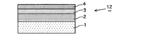
- FIG. 2 is a schematic diagram of a reflective mask blank 12 for EUV lithography according to the present invention.
- the mask blank 12 of the present invention is obtained by forming the absorber film 4 that absorbs EUV light on the protective film 3 of the substrate 10 with the multilayer reflective film of the present invention described above.
- a predetermined absorber film pattern is obtained, and a portion that reflects light (EUV light in the present invention) (a portion where the protective film 3 and the multilayer reflective film 2 below it are exposed)
- a reflective mask for EUV lithography having a light absorbing portion (absorber film pattern) is obtained.
- a back conductive film may be formed on the surface of the substrate 1 opposite to the surface in contact with the multilayer reflective film 2 for the purpose of electrostatic chuck as described above.
- the electrical characteristics required for the back conductive film are usually 100 ⁇ / ⁇ or less.
- a method for forming the back conductive film is known, and can be formed by using a target of metal or alloy such as chromium (Cr) or tantalum (Ta), for example, by magnetron sputtering or ion beam sputtering.
- the thickness of the back conductive film is not particularly limited as long as the above object is achieved, but it is usually 10 to 200 nm.
- the constituent material of the absorber film 4 is not particularly limited as long as it has a function of absorbing the EUV light and can be removed by etching or the like (preferably, it can be etched by dry etching of chlorine (Cl) gas).
- a tantalum (Ta) simple substance or a tantalum compound containing Ta as a main component can be preferably used.
- the tantalum compound is usually a Ta alloy.
- the crystalline state of the absorber film 4 is preferably an amorphous or microcrystalline structure from the viewpoint of smoothness and flatness. If the surface of the absorber film 4 is not smooth and flat, the edge roughness of the absorber film pattern increases, and the dimensional accuracy of the pattern may deteriorate.
- the surface roughness of the absorber film 4 is preferably 0.5 nmRms or less, more preferably 0.4 nmRms or less and 0.3 nmRms or less.
- a compound containing Ta and B a compound containing Ta and N, a compound containing Ta and B and further containing at least one of O and N, a compound containing Ta and Si, Ta A compound containing Si and N, a compound containing Ta and Ge, a compound containing Ta, Ge and N, and the like can be used.
- Ta is a material that has a large EUV light absorption coefficient and can be easily dry-etched with a chlorine-based gas, it is an absorber film material that is excellent in light absorption and workability. Furthermore, by adding B, Si, Ge or the like to Ta, an amorphous material can be easily obtained, and the smoothness of the absorber film 4 can be improved. Further, when N or O is added to Ta, the resistance of the absorber film 4 to oxidation is improved, so that it is possible to improve the stability over time.
- the absorber film material can be microcrystallized by adjusting the substrate heating temperature during the formation of the absorber film 4 and the sputtering gas pressure during the film formation.
- the absorber film 4 described above has a thickness of the absorber film 4 small when the absorption coefficient is 0.025 or more, further 0.030 or more (usually 0.080 or less) with respect to the wavelength of the exposure light. It is preferable in that it can be performed.
- the thickness of the absorber film 4 may be any thickness that can sufficiently absorb EUV light as exposure light, but is usually about 30 to 100 nm.
- the absorber film 4 can be formed by a known method such as a sputtering method such as magnetron sputtering.
- the absorber film 4 can be formed on the protective film 3 by a sputtering method using a target containing tantalum and boron and using an argon gas to which oxygen or nitrogen is added.
- a resist film is formed on the absorber film 4 of the mask blank 12 (FIG. 3A), a desired pattern is drawn (exposure) thereon, and further developed and rinsed to obtain a predetermined resist pattern. 5a is formed.
- this resist pattern 5a As a mask and performing dry etching with a chlorine-based gas, the portion of the absorber film 4 that is not covered with the resist pattern 5a is etched, and the absorber film pattern 4a becomes the protective film 3. It is formed on the top (FIG. 3B).
- the protective film 3 is also dry-etched.
- a specific alloy that is a solid solution is used as a protective film material. Therefore, the protective film 3 is very stable against the etching gas, and there is almost no film loss or disappearance in the subsequent wet cleaning (including wet cleaning in the process of using the reflective mask). Very few. Therefore, the multilayer reflective film 2 under the protective film 3 is not damaged, and an excellent reflectance is achieved and maintained.
- chlorine-based gas chlorine alone gas, mixed gas containing chlorine and oxygen in a predetermined ratio, mixed gas containing chlorine and helium in a predetermined ratio, mixed gas containing chlorine and argon in a predetermined ratio, In addition, a mixed gas containing chlorine and boron trichloride in a predetermined ratio can be given.
- a reflective mask 20 for EUV lithography that achieves the above is obtained (FIG. 3C).
- the obtained reflective mask 20 for EUV lithography is usually subjected to pattern inspection and correction.
- the above-described wet cleaning is usually performed even after pattern inspection and correction.
- the wet cleaning method is appropriately selected depending on the object to be removed. Examples of wet cleaning include acid / alkaline cleaning using sulfuric acid / water (SPM) and ammonia water (APM), functional water cleaning using ozone water, ammonia-added hydrogen water, scrub cleaning and MHz order Examples include megasonic cleaning using ultrasonic waves.
- a transfer pattern based on the absorber film pattern of the mask is formed on a transfer target such as a semiconductor substrate, and various other processes are performed on the semiconductor substrate.
- a semiconductor device in which the pattern or the like is formed can be manufactured.
- the pattern transfer apparatus 50 equipped with the reflective mask 20 is roughly composed of a laser plasma X-ray source 31, a reflective mask 20, a reduction optical system 32, and the like.
- the reduction optical system 32 an X-ray reflection mirror is used.
- the pattern reflected by the reflective mask 20 is usually reduced to about 1 ⁇ 4 by the reduction optical system 32.
- a wavelength band of 13 to 14 nm is used as the exposure wavelength, and the optical path is preset so as to be a vacuum.
- EUV light obtained from the laser plasma X-ray source 31 is incident on the reflective mask 20, and the light reflected here is transferred onto the semiconductor substrate 33 with resist through the reduction optical system 32.
- the light incident on the reflective mask 20 is absorbed and not reflected by the absorber film at a portion where the absorber film pattern 4a is present, while the light incident on the portion where the absorber film pattern 4a is not present is reflected by the multilayer reflective film 2. It is reflected by. In this way, an image formed by the light reflected from the reflective mask 20 enters the reduction optical system 32.
- the exposure light passing through the reduction optical system 32 forms a transfer pattern on the resist layer on the semiconductor substrate 33 with resist.
- the resist pattern can be formed on the semiconductor substrate 33 with resist by developing the exposed resist layer.
- a predetermined wiring pattern can be formed on the semiconductor substrate.
- a semiconductor device is manufactured through such a process and other necessary processes.
- Protective film formation conditions Ru target, sputtering in Ar gas atmosphere, film thickness 14 nm.
- Example sample 1 In the same manner as in Comparative Sample 1, a RuCo (Ru: 97 atomic%, Co: 3 atomic%) protective film was formed on the main surface of the substrate.
- the protective film formation conditions are the same as those of Comparative Example Sample 1 except that a Ru97Co3 target (the numerical value is an atomic% ratio) is used. Note that the composition of each element constituting the protective film is a value measured by Auger electron spectroscopy. The same applies to Example Samples 2 to 5 and Comparative Sample 2.
- Example sample 2 In the same manner as in Comparative Example Sample 1, a RuCo (Ru: 90 atomic%, Co: 10 atomic%) protective film was formed on the main surface of the substrate.
- the protective film formation conditions are the same as those of Comparative Example Sample 1 except that a Ru90Co10 target (the numerical value is an atomic percentage) is used.
- Example sample 3 A RuCo (Ru: 75 atomic%, Co: 25 atomic%) protective film was formed on the main surface of the substrate in the same manner as in Comparative Example Sample 1.
- the protective film formation conditions are the same as those of Comparative Example Sample 1 except that a Ru75Co25 target (the numerical value is an atomic percentage) is used.
- Example Sample 4 A RuCo (Ru: 50 atomic%, Co: 50 atomic%) protective film was formed on the main surface of the substrate in the same manner as in Comparative Example Sample 1.
- the protective film formation conditions are the same as those of Comparative Example Sample 1 except that a Ru50Co50 target (the numerical value is an atomic percentage) is used.
- Example Sample 5 In the same manner as Comparative Example Sample 1, a RuRe (Ru: 97 atomic%, Re: 3 atomic%) protective film was formed on the main surface of the substrate.
- the protective film formation conditions are the same as those of Comparative Example Sample 1 except that a Ru97Re3 target (the numerical value is an atomic percentage) is used.
- Comparative sample 2 In the same manner as in Comparative Example Sample 1, a RuZr (Ru: 80 atomic%, Zr: 20 atomic%) protective film (RuZr is not a total solid solution) was formed on the main surface of the substrate.
- the protective film formation conditions are the same as those of Comparative Example Sample 1 except that a Ru80Zr20 target (the numerical value is an atomic percentage) is used.
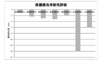
- the film thickness of the protective film after the wet cleaning was measured by XRR, the change in film thickness due to the wet cleaning was measured, and the protective film cleaning resistance of each sample was evaluated.
- Example Sample 1 ( ⁇ 1.0 nm), Example Sample 2 (-2.3 nm), Example sample 3 (-2.9 nm), Example sample 4 (-3.2 nm), and Example sample 5 (-1.8 nm).
- Example Sample 2 ( ⁇ 1.0 nm)
- Example Sample 2 (-2.3 nm)
- Example sample 3 (-2.9 nm)
- Example sample 4 (-3.2 nm)
- Example sample 5 (-1.8 nm).
- Example 1 Production of substrate with multilayer reflective film Using a polishing liquid containing colloidal silica abrasive grains on both main surfaces of a TiO 2 -SiO 2 glass (low thermal expansion glass) substrate having a size of 152 mm x 152 mm Then, the substrate was precisely polished and washed to obtain a substrate having a flatness of 0.05 ⁇ m and a surface roughness Rms (root mean square roughness) of 0.12 nm. A multilayer reflective film was formed on the main surface of this substrate by ion beam sputtering (Mo target, Si target).
- Multilayer reflective film Si (4.2 nm) / Mo (2.8 nm) as one period, 40 periods (Si) film is in contact with the main surface of the substrate: total film thickness 280 nm
- Example Sample 1 On the formed multilayer reflective film, the RuCo protective film (Ru: 97 atomic%, Co: 3 atomic%) of Example Sample 1 was formed by the magnetron sputtering method to obtain a substrate with the multilayer reflective film.
- the protective film had a thickness of 2.5 nm.
- the reflectance of EUV light (wavelength: 13.5 nm) was measured for this substrate with a multilayer reflective film using an EUV reflectance measuring apparatus, the reflectance was as high as 66%.
- Example 2 A substrate with a multilayer reflective film was formed in the same manner as in Example 1 except that the protective film was RuCo (Ru: 90 atomic%, Co: 10 atomic%) and the film thickness was 2.5 nm. The reflectance of the EUV light was 65%.
- Example 3 A substrate with a multilayer reflective film was formed in the same manner as in Example 1 except that the protective film was RuCo (Ru: 75 atomic%, Co: 25 atomic%) and the film thickness was 2.5 nm. The reflectance of the EUV light was 64%.
- Example 4 A substrate with a multilayer reflective film was formed in the same manner as in Example 1 except that the protective film was RuRe (Ru: 97 atomic%, Re: 3 atomic%) and the film thickness was 2.5 nm. The reflectance of the EUV light was 65%.
- TaBN film an absorber film
- Example 6 Fabrication of a reflective mask A resist film was applied on the absorber film of the reflective mask blank obtained in Example 5 by spin coating, heated and cooled to form a resist film (film thickness 120 nm). did.
- a predetermined pattern was drawn and developed on the resist film to form a resist pattern.
- the absorber film which is a TaBN film
- any of the reflective masks prepared from the substrates with multilayer reflective films of Examples 1 to 4 disappearance of the protective film was not confirmed, and all the EUV light reflectances were maintained at a high reflectance of 64% or more. The same result was obtained for the reflectance even after the wet cleaning was repeated three times. Therefore, when the lithography process using the pattern transfer apparatus is performed using the reflective masks of Examples 1 to 4, the EUV light is reflected on each film surface and the protective film surface constituting the multilayer reflective film; Since a high contrast can be maintained with the absorption of EUV light in the absorber film pattern, for example, a semiconductor device having a desired circuit pattern can be manufactured.
- Example 6 In Example 6, when the reflective masks were prepared using the comparative samples 1 and 2 as the protective film, all of the protective film disappeared in the mask, and the reflectance of the EUV light of the mask was also changed to the multilayer reflective film. It was reduced to 60% due to damage.
Landscapes
- Engineering & Computer Science (AREA)
- Physics & Mathematics (AREA)
- Chemical & Material Sciences (AREA)
- Nanotechnology (AREA)
- General Physics & Mathematics (AREA)
- Crystallography & Structural Chemistry (AREA)
- Mathematical Physics (AREA)
- Theoretical Computer Science (AREA)
- Condensed Matter Physics & Semiconductors (AREA)
- Manufacturing & Machinery (AREA)
- Preparing Plates And Mask In Photomechanical Process (AREA)
- Exposure Of Semiconductors, Excluding Electron Or Ion Beam Exposure (AREA)
Abstract
Priority Applications (3)
| Application Number | Priority Date | Filing Date | Title |
|---|---|---|---|
| US14/373,715 US9383637B2 (en) | 2012-03-23 | 2013-03-21 | Substrate with multilayer reflective film, reflective mask blank for EUV lithography, method of manufacturing reflective mask for EUV lithography and method of manufacturing semiconductor device |
| KR1020147019934A KR102124176B1 (ko) | 2012-03-23 | 2013-03-21 | 다층 반사막 부착 기판, euv 리소그래피용 반사형 마스크 블랭크, euv 리소그래피용 반사형 마스크의 제조 방법 및 반도체 장치의 제조 방법 |
| JP2014506260A JP6082385B2 (ja) | 2012-03-23 | 2013-03-21 | 多層反射膜付き基板、euvリソグラフィー用反射型マスクブランク、euvリソグラフィー用反射型マスクの製造方法、及び半導体装置の製造方法 |
Applications Claiming Priority (2)
| Application Number | Priority Date | Filing Date | Title |
|---|---|---|---|
| JP2012-067142 | 2012-03-23 | ||
| JP2012067142 | 2012-03-23 |
Publications (1)
| Publication Number | Publication Date |
|---|---|
| WO2013141268A1 true WO2013141268A1 (fr) | 2013-09-26 |
Family
ID=49222725
Family Applications (1)
| Application Number | Title | Priority Date | Filing Date |
|---|---|---|---|
| PCT/JP2013/057957 Ceased WO2013141268A1 (fr) | 2012-03-23 | 2013-03-21 | Substrat avec film réfléchissant multicouche, ébauche de masque réfléchissant pour la lithographie euv, procédé de production d'une ébauche réfléchissante pour la lithographie euv, et procédé de fabrication d'un dispositif à semi-conducteur |
Country Status (5)
| Country | Link |
|---|---|
| US (1) | US9383637B2 (fr) |
| JP (1) | JP6082385B2 (fr) |
| KR (1) | KR102124176B1 (fr) |
| TW (1) | TWI587078B (fr) |
| WO (1) | WO2013141268A1 (fr) |
Cited By (3)
| Publication number | Priority date | Publication date | Assignee | Title |
|---|---|---|---|---|
| JP2015056423A (ja) * | 2013-09-10 | 2015-03-23 | Hoya株式会社 | 多層反射膜付き基板、euvリソグラフィー用反射型マスクブランク、euvリソグラフィー用反射型マスク及びその製造方法、並びに半導体装置の製造方法 |
| WO2015095808A1 (fr) * | 2013-12-22 | 2015-06-25 | Applied Materials, Inc. | Système de lithographie par rayonnement ultraviolet extrême comprenant un ensemble mandrin et son procédé de fabrication |
| JP2019116682A (ja) * | 2017-12-27 | 2019-07-18 | 光洋應用材料科技股▲分▼有限公司 | ルテニウム/レニウムを含むスパッタリングターゲット、ルテニウム/レニウムを含む層およびその製法 |
Families Citing this family (7)
| Publication number | Priority date | Publication date | Assignee | Title |
|---|---|---|---|---|
| WO2011039811A1 (fr) * | 2009-09-30 | 2011-04-07 | Necディスプレイソリューションズ株式会社 | Dispositif de traitement de signal d'image et procédé de traitement de signal d'image |
| US9739913B2 (en) * | 2014-07-11 | 2017-08-22 | Applied Materials, Inc. | Extreme ultraviolet capping layer and method of manufacturing and lithography thereof |
| CN104732911B (zh) * | 2015-04-09 | 2017-03-15 | 京东方科技集团股份有限公司 | 显示驱动方法、驱动电路和显示装置 |
| KR102741625B1 (ko) * | 2016-11-22 | 2024-12-16 | 삼성전자주식회사 | 극자외선 리소그래피용 위상 반전 마스크 |
| KR20220022474A (ko) | 2019-06-20 | 2022-02-25 | 호야 가부시키가이샤 | 반사형 마스크 블랭크, 반사형 마스크, 그리고 반사형 마스크 및 반도체 장치의 제조 방법 |
| US12353120B2 (en) * | 2021-07-30 | 2025-07-08 | Taiwan Semiconductor Manufacturing Company, Ltd. | EUV photo masks and manufacturing method thereof |
| WO2024010631A1 (fr) * | 2022-07-05 | 2024-01-11 | Fujifilm Electronic Materials U.S.A., Inc. | Compositions de nettoyage |
Citations (4)
| Publication number | Priority date | Publication date | Assignee | Title |
|---|---|---|---|---|
| JP2002353123A (ja) * | 2001-05-29 | 2002-12-06 | Toppan Printing Co Ltd | 反射型投影露光マスク |
| JP2004171034A (ja) * | 2004-03-22 | 2004-06-17 | Hoya Corp | 積層体 |
| JP2007294840A (ja) * | 2006-03-30 | 2007-11-08 | Toppan Printing Co Ltd | 反射型フォトマスクブランク及びその製造方法、反射型フォトマスク、並びに、半導体装置の製造方法 |
| JP2011192693A (ja) * | 2010-03-12 | 2011-09-29 | Hoya Corp | 多層反射膜付基板、反射型マスクブランク及びそれらの製造方法 |
Family Cites Families (12)
| Publication number | Priority date | Publication date | Assignee | Title |
|---|---|---|---|---|
| US5013681A (en) * | 1989-09-29 | 1991-05-07 | The United States Of America As Represented By The Secretary Of The Navy | Method of producing a thin silicon-on-insulator layer |
| JP5371162B2 (ja) | 2000-10-13 | 2013-12-18 | 三星電子株式会社 | 反射型フォトマスク |
| DE10150874A1 (de) * | 2001-10-04 | 2003-04-30 | Zeiss Carl | Optisches Element und Verfahren zu dessen Herstellung sowie ein Lithographiegerät und ein Verfahren zur Herstellung eines Halbleiterbauelements |
| EP2317383A3 (fr) * | 2002-04-11 | 2011-12-28 | HOYA Corporation | Ébauche de masque réfléchissant, masque réfléchissant et procédés de fabrication de l'ébauche de masque et masque |
| JP2006171577A (ja) * | 2004-12-17 | 2006-06-29 | Nikon Corp | 光学素子及びこれを用いた投影露光装置 |
| JP2006173502A (ja) * | 2004-12-17 | 2006-06-29 | Nikon Corp | 光学素子及びこれを用いた投影露光装置 |
| JP2007127698A (ja) * | 2005-11-01 | 2007-05-24 | Nikon Corp | 多層膜反射鏡、その再生方法および露光装置 |
| JP4910856B2 (ja) | 2006-06-08 | 2012-04-04 | 旭硝子株式会社 | Euvリソグラフィ用反射型マスクブランク、および該マスクブランク用の機能膜付基板 |
| KR20110065439A (ko) * | 2008-09-05 | 2011-06-15 | 아사히 가라스 가부시키가이샤 | Euv 리소그래피용 반사형 마스크 블랭크 및 그 제조 방법 |
| CN102203907B (zh) * | 2008-10-30 | 2014-03-26 | 旭硝子株式会社 | Euv光刻用反射型掩模基板 |
| JP2012009537A (ja) * | 2010-06-23 | 2012-01-12 | Dainippon Printing Co Ltd | 反射型マスクブランクス、反射型マスク、反射型マスクブランクスの製造方法、および、反射型マスクの製造方法 |
| KR20130111524A (ko) * | 2010-07-27 | 2013-10-10 | 아사히 가라스 가부시키가이샤 | Euv 리소그래피용 반사층 형성 기판, 및 euv 리소그래피용 반사형 마스크 블랭크 |
-
2013
- 2013-03-21 WO PCT/JP2013/057957 patent/WO2013141268A1/fr not_active Ceased
- 2013-03-21 JP JP2014506260A patent/JP6082385B2/ja active Active
- 2013-03-21 US US14/373,715 patent/US9383637B2/en active Active
- 2013-03-21 KR KR1020147019934A patent/KR102124176B1/ko active Active
- 2013-03-22 TW TW102110169A patent/TWI587078B/zh active
Patent Citations (4)
| Publication number | Priority date | Publication date | Assignee | Title |
|---|---|---|---|---|
| JP2002353123A (ja) * | 2001-05-29 | 2002-12-06 | Toppan Printing Co Ltd | 反射型投影露光マスク |
| JP2004171034A (ja) * | 2004-03-22 | 2004-06-17 | Hoya Corp | 積層体 |
| JP2007294840A (ja) * | 2006-03-30 | 2007-11-08 | Toppan Printing Co Ltd | 反射型フォトマスクブランク及びその製造方法、反射型フォトマスク、並びに、半導体装置の製造方法 |
| JP2011192693A (ja) * | 2010-03-12 | 2011-09-29 | Hoya Corp | 多層反射膜付基板、反射型マスクブランク及びそれらの製造方法 |
Cited By (4)
| Publication number | Priority date | Publication date | Assignee | Title |
|---|---|---|---|---|
| JP2015056423A (ja) * | 2013-09-10 | 2015-03-23 | Hoya株式会社 | 多層反射膜付き基板、euvリソグラフィー用反射型マスクブランク、euvリソグラフィー用反射型マスク及びその製造方法、並びに半導体装置の製造方法 |
| WO2015095808A1 (fr) * | 2013-12-22 | 2015-06-25 | Applied Materials, Inc. | Système de lithographie par rayonnement ultraviolet extrême comprenant un ensemble mandrin et son procédé de fabrication |
| US10691013B2 (en) | 2013-12-22 | 2020-06-23 | Applied Materials, Inc. | Extreme ultraviolet lithography system having chuck assembly and method of manufacturing thereof |
| JP2019116682A (ja) * | 2017-12-27 | 2019-07-18 | 光洋應用材料科技股▲分▼有限公司 | ルテニウム/レニウムを含むスパッタリングターゲット、ルテニウム/レニウムを含む層およびその製法 |
Also Published As
| Publication number | Publication date |
|---|---|
| TWI587078B (zh) | 2017-06-11 |
| US9383637B2 (en) | 2016-07-05 |
| KR20140138601A (ko) | 2014-12-04 |
| US20140370424A1 (en) | 2014-12-18 |
| KR102124176B1 (ko) | 2020-06-17 |
| TW201348856A (zh) | 2013-12-01 |
| JP6082385B2 (ja) | 2017-02-15 |
| JPWO2013141268A1 (ja) | 2015-08-03 |
Similar Documents
| Publication | Publication Date | Title |
|---|---|---|
| JP6082385B2 (ja) | 多層反射膜付き基板、euvリソグラフィー用反射型マスクブランク、euvリソグラフィー用反射型マスクの製造方法、及び半導体装置の製造方法 | |
| JP6470176B2 (ja) | 多層反射膜付き基板、euvリソグラフィー用反射型マスクブランク、euvリソグラフィー用反射型マスク及びその製造方法、並びに半導体装置の製造方法 | |
| JP7605362B2 (ja) | Euvリソグラフィ用反射型マスクブランク、euvリソグラフィ用反射型マスク、およびそれらの製造方法 | |
| TWI881058B (zh) | 反射型光罩基底及反射型光罩、與半導體裝置之製造方法 | |
| JP6422873B2 (ja) | 多層反射膜付き基板、euvリソグラフィー用反射型マスクブランク、euvリソグラフィー用反射型マスク及びその製造方法、並びに半導体装置の製造方法 | |
| JP6184026B2 (ja) | 反射型マスクブランク及びその製造方法、反射型マスクの製造方法、並びに半導体装置の製造方法 | |
| JP4521753B2 (ja) | 反射型マスクの製造方法及び半導体装置の製造方法 | |
| WO2022138434A1 (fr) | Substrat équipé d'un film réfléchissant multicouche, ébauche de masque réfléchissant, masque réfléchissant et procédé de production d'un dispositif à semi-conducteur | |
| TW202122907A (zh) | 附導電膜之基板、反射型光罩基底及反射型光罩、以及半導體裝置之製造方法 | |
| WO2021200325A1 (fr) | Substrat équipé d'un film réfléchissant multicouche, ébauche de masque réfléchissant, masque réfléchissant et procédé de production d'un dispositif à semi-conducteur | |
| TW202527069A (zh) | 反射型光罩基底、反射型光罩、及半導體裝置之製造方法 | |
| JP7743590B2 (ja) | 反射型マスクブランク、反射型マスク、反射型マスクの製造方法、及び半導体装置の製造方法 | |
| JP2026034634A (ja) | 多層反射膜付き基板、反射型マスクブランク、反射型マスクの製造方法、及び半導体装置の製造方法 | |
| JP4390418B2 (ja) | Euv露光用反射型マスクブランクおよびeuv露光用反射型マスク並びに半導体の製造方法 | |
| JP2003249434A (ja) | 露光用反射型マスクブランク及び露光用反射型マスク | |
| JP6223756B2 (ja) | 多層反射膜付き基板、euvリソグラフィー用反射型マスクブランク、euvリソグラフィー用反射型マスク及びその製造方法、並びに半導体装置の製造方法 | |
| JP4541654B2 (ja) | 反射型マスクの製造方法 | |
| WO2022149417A1 (fr) | Substrat d'ébauche de masque, substrat à film réfléchissant multicouche, ébauche de masque, procédé de fabrication de masque de transfert et procédé de fabrication de dispositif semi-conducteur | |
| KR20250164715A (ko) | 반사형 마스크 블랭크, 반사형 마스크 블랭크의 제조 방법, 반사형 마스크, 반사형 마스크의 제조 방법 |
Legal Events
| Date | Code | Title | Description |
|---|---|---|---|
| 121 | Ep: the epo has been informed by wipo that ep was designated in this application |
Ref document number: 13764234 Country of ref document: EP Kind code of ref document: A1 |
|
| ENP | Entry into the national phase |
Ref document number: 2014506260 Country of ref document: JP Kind code of ref document: A |
|
| ENP | Entry into the national phase |
Ref document number: 20147019934 Country of ref document: KR Kind code of ref document: A |
|
| WWE | Wipo information: entry into national phase |
Ref document number: 14373715 Country of ref document: US |
|
| NENP | Non-entry into the national phase |
Ref country code: DE |
|
| 122 | Ep: pct application non-entry in european phase |
Ref document number: 13764234 Country of ref document: EP Kind code of ref document: A1 |