WO2013146881A1 - パワーモジュール用基板及びその製造方法 - Google Patents
パワーモジュール用基板及びその製造方法 Download PDFInfo
- Publication number
- WO2013146881A1 WO2013146881A1 PCT/JP2013/059001 JP2013059001W WO2013146881A1 WO 2013146881 A1 WO2013146881 A1 WO 2013146881A1 JP 2013059001 W JP2013059001 W JP 2013059001W WO 2013146881 A1 WO2013146881 A1 WO 2013146881A1
- Authority
- WO
- WIPO (PCT)
- Prior art keywords
- metal plate
- power module
- ceramic substrate
- substrate
- manufacturing
- Prior art date
- Legal status (The legal status is an assumption and is not a legal conclusion. Google has not performed a legal analysis and makes no representation as to the accuracy of the status listed.)
- Ceased
Links
Images


Classifications
-
- B—PERFORMING OPERATIONS; TRANSPORTING
- B23—MACHINE TOOLS; METAL-WORKING NOT OTHERWISE PROVIDED FOR
- B23K—SOLDERING OR UNSOLDERING; WELDING; CLADDING OR PLATING BY SOLDERING OR WELDING; CUTTING BY APPLYING HEAT LOCALLY, e.g. FLAME CUTTING; WORKING BY LASER BEAM
- B23K1/00—Soldering, e.g. brazing, or unsoldering
- B23K1/0008—Soldering, e.g. brazing, or unsoldering specially adapted for particular articles or work
- B23K1/0016—Soldering of electronic components
-
- B—PERFORMING OPERATIONS; TRANSPORTING
- B23—MACHINE TOOLS; METAL-WORKING NOT OTHERWISE PROVIDED FOR
- B23K—SOLDERING OR UNSOLDERING; WELDING; CLADDING OR PLATING BY SOLDERING OR WELDING; CUTTING BY APPLYING HEAT LOCALLY, e.g. FLAME CUTTING; WORKING BY LASER BEAM
- B23K1/00—Soldering, e.g. brazing, or unsoldering
- B23K1/19—Soldering, e.g. brazing, or unsoldering taking account of the properties of the materials to be soldered
-
- B—PERFORMING OPERATIONS; TRANSPORTING
- B32—LAYERED PRODUCTS
- B32B—LAYERED PRODUCTS, i.e. PRODUCTS BUILT-UP OF STRATA OF FLAT OR NON-FLAT, e.g. CELLULAR OR HONEYCOMB, FORM
- B32B15/00—Layered products comprising a layer of metal
- B32B15/04—Layered products comprising a layer of metal comprising metal as the main or only constituent of a layer, which is next to another layer of the same or of a different material
-
- B—PERFORMING OPERATIONS; TRANSPORTING
- B32—LAYERED PRODUCTS
- B32B—LAYERED PRODUCTS, i.e. PRODUCTS BUILT-UP OF STRATA OF FLAT OR NON-FLAT, e.g. CELLULAR OR HONEYCOMB, FORM
- B32B18/00—Layered products essentially comprising ceramics, e.g. refractory products
-
- C—CHEMISTRY; METALLURGY
- C04—CEMENTS; CONCRETE; ARTIFICIAL STONE; CERAMICS; REFRACTORIES
- C04B—LIME, MAGNESIA; SLAG; CEMENTS; COMPOSITIONS THEREOF, e.g. MORTARS, CONCRETE OR LIKE BUILDING MATERIALS; ARTIFICIAL STONE; CERAMICS; REFRACTORIES; TREATMENT OF NATURAL STONE
- C04B37/00—Joining burned ceramic articles with other burned ceramic articles or other articles by heating
- C04B37/02—Joining burned ceramic articles with other burned ceramic articles or other articles by heating with metallic articles
- C04B37/023—Joining burned ceramic articles with other burned ceramic articles or other articles by heating with metallic articles characterised by the interlayer used
- C04B37/026—Joining burned ceramic articles with other burned ceramic articles or other articles by heating with metallic articles characterised by the interlayer used consisting of metals or metal salts
-
- H—ELECTRICITY
- H05—ELECTRIC TECHNIQUES NOT OTHERWISE PROVIDED FOR
- H05K—PRINTED CIRCUITS; CASINGS OR CONSTRUCTIONAL DETAILS OF ELECTRIC APPARATUS; MANUFACTURE OF ASSEMBLAGES OF ELECTRICAL COMPONENTS
- H05K3/00—Apparatus or processes for manufacturing printed circuits
- H05K3/38—Improvement of the adhesion between the insulating substrate and the metal
- H05K3/382—Improvement of the adhesion between the insulating substrate and the metal by special treatment of the metal
- H05K3/383—Improvement of the adhesion between the insulating substrate and the metal by special treatment of the metal by microetching
-
- H—ELECTRICITY
- H10—SEMICONDUCTOR DEVICES; ELECTRIC SOLID-STATE DEVICES NOT OTHERWISE PROVIDED FOR
- H10W—GENERIC PACKAGES, INTERCONNECTIONS, CONNECTORS OR OTHER CONSTRUCTIONAL DETAILS OF DEVICES COVERED BY CLASS H10
- H10W40/00—Arrangements for thermal protection or thermal control
- H10W40/20—Arrangements for cooling
- H10W40/25—Arrangements for cooling characterised by their materials
- H10W40/255—Arrangements for cooling characterised by their materials having a laminate or multilayered structure, e.g. direct bond copper [DBC] ceramic substrates
-
- B—PERFORMING OPERATIONS; TRANSPORTING
- B32—LAYERED PRODUCTS
- B32B—LAYERED PRODUCTS, i.e. PRODUCTS BUILT-UP OF STRATA OF FLAT OR NON-FLAT, e.g. CELLULAR OR HONEYCOMB, FORM
- B32B2457/00—Electrical equipment
-
- C—CHEMISTRY; METALLURGY
- C04—CEMENTS; CONCRETE; ARTIFICIAL STONE; CERAMICS; REFRACTORIES
- C04B—LIME, MAGNESIA; SLAG; CEMENTS; COMPOSITIONS THEREOF, e.g. MORTARS, CONCRETE OR LIKE BUILDING MATERIALS; ARTIFICIAL STONE; CERAMICS; REFRACTORIES; TREATMENT OF NATURAL STONE
- C04B2235/00—Aspects relating to ceramic starting mixtures or sintered ceramic products
- C04B2235/65—Aspects relating to heat treatments of ceramic bodies such as green ceramics or pre-sintered ceramics, e.g. burning, sintering or melting processes
- C04B2235/658—Atmosphere during thermal treatment
- C04B2235/6581—Total pressure below 1 atmosphere, e.g. vacuum
-
- C—CHEMISTRY; METALLURGY
- C04—CEMENTS; CONCRETE; ARTIFICIAL STONE; CERAMICS; REFRACTORIES
- C04B—LIME, MAGNESIA; SLAG; CEMENTS; COMPOSITIONS THEREOF, e.g. MORTARS, CONCRETE OR LIKE BUILDING MATERIALS; ARTIFICIAL STONE; CERAMICS; REFRACTORIES; TREATMENT OF NATURAL STONE
- C04B2235/00—Aspects relating to ceramic starting mixtures or sintered ceramic products
- C04B2235/70—Aspects relating to sintered or melt-casted ceramic products
- C04B2235/72—Products characterised by the absence or the low content of specific components, e.g. alkali metal free alumina ceramics
- C04B2235/723—Oxygen content
-
- C—CHEMISTRY; METALLURGY
- C04—CEMENTS; CONCRETE; ARTIFICIAL STONE; CERAMICS; REFRACTORIES
- C04B—LIME, MAGNESIA; SLAG; CEMENTS; COMPOSITIONS THEREOF, e.g. MORTARS, CONCRETE OR LIKE BUILDING MATERIALS; ARTIFICIAL STONE; CERAMICS; REFRACTORIES; TREATMENT OF NATURAL STONE
- C04B2235/00—Aspects relating to ceramic starting mixtures or sintered ceramic products
- C04B2235/70—Aspects relating to sintered or melt-casted ceramic products
- C04B2235/96—Properties of ceramic products, e.g. mechanical properties such as strength, toughness, wear resistance
- C04B2235/963—Surface properties, e.g. surface roughness
-
- C—CHEMISTRY; METALLURGY
- C04—CEMENTS; CONCRETE; ARTIFICIAL STONE; CERAMICS; REFRACTORIES
- C04B—LIME, MAGNESIA; SLAG; CEMENTS; COMPOSITIONS THEREOF, e.g. MORTARS, CONCRETE OR LIKE BUILDING MATERIALS; ARTIFICIAL STONE; CERAMICS; REFRACTORIES; TREATMENT OF NATURAL STONE
- C04B2237/00—Aspects relating to ceramic laminates or to joining of ceramic articles with other articles by heating
- C04B2237/02—Aspects relating to interlayers, e.g. used to join ceramic articles with other articles by heating
- C04B2237/04—Ceramic interlayers
- C04B2237/06—Oxidic interlayers
- C04B2237/064—Oxidic interlayers based on alumina or aluminates
-
- C—CHEMISTRY; METALLURGY
- C04—CEMENTS; CONCRETE; ARTIFICIAL STONE; CERAMICS; REFRACTORIES
- C04B—LIME, MAGNESIA; SLAG; CEMENTS; COMPOSITIONS THEREOF, e.g. MORTARS, CONCRETE OR LIKE BUILDING MATERIALS; ARTIFICIAL STONE; CERAMICS; REFRACTORIES; TREATMENT OF NATURAL STONE
- C04B2237/00—Aspects relating to ceramic laminates or to joining of ceramic articles with other articles by heating
- C04B2237/02—Aspects relating to interlayers, e.g. used to join ceramic articles with other articles by heating
- C04B2237/12—Metallic interlayers
- C04B2237/121—Metallic interlayers based on aluminium
-
- C—CHEMISTRY; METALLURGY
- C04—CEMENTS; CONCRETE; ARTIFICIAL STONE; CERAMICS; REFRACTORIES
- C04B—LIME, MAGNESIA; SLAG; CEMENTS; COMPOSITIONS THEREOF, e.g. MORTARS, CONCRETE OR LIKE BUILDING MATERIALS; ARTIFICIAL STONE; CERAMICS; REFRACTORIES; TREATMENT OF NATURAL STONE
- C04B2237/00—Aspects relating to ceramic laminates or to joining of ceramic articles with other articles by heating
- C04B2237/02—Aspects relating to interlayers, e.g. used to join ceramic articles with other articles by heating
- C04B2237/12—Metallic interlayers
- C04B2237/126—Metallic interlayers wherein the active component for bonding is not the largest fraction of the interlayer
- C04B2237/128—The active component for bonding being silicon
-
- C—CHEMISTRY; METALLURGY
- C04—CEMENTS; CONCRETE; ARTIFICIAL STONE; CERAMICS; REFRACTORIES
- C04B—LIME, MAGNESIA; SLAG; CEMENTS; COMPOSITIONS THEREOF, e.g. MORTARS, CONCRETE OR LIKE BUILDING MATERIALS; ARTIFICIAL STONE; CERAMICS; REFRACTORIES; TREATMENT OF NATURAL STONE
- C04B2237/00—Aspects relating to ceramic laminates or to joining of ceramic articles with other articles by heating
- C04B2237/30—Composition of layers of ceramic laminates or of ceramic or metallic articles to be joined by heating, e.g. Si substrates
- C04B2237/32—Ceramic
- C04B2237/36—Non-oxidic
- C04B2237/366—Aluminium nitride
-
- C—CHEMISTRY; METALLURGY
- C04—CEMENTS; CONCRETE; ARTIFICIAL STONE; CERAMICS; REFRACTORIES
- C04B—LIME, MAGNESIA; SLAG; CEMENTS; COMPOSITIONS THEREOF, e.g. MORTARS, CONCRETE OR LIKE BUILDING MATERIALS; ARTIFICIAL STONE; CERAMICS; REFRACTORIES; TREATMENT OF NATURAL STONE
- C04B2237/00—Aspects relating to ceramic laminates or to joining of ceramic articles with other articles by heating
- C04B2237/30—Composition of layers of ceramic laminates or of ceramic or metallic articles to be joined by heating, e.g. Si substrates
- C04B2237/40—Metallic
- C04B2237/402—Aluminium
-
- C—CHEMISTRY; METALLURGY
- C04—CEMENTS; CONCRETE; ARTIFICIAL STONE; CERAMICS; REFRACTORIES
- C04B—LIME, MAGNESIA; SLAG; CEMENTS; COMPOSITIONS THEREOF, e.g. MORTARS, CONCRETE OR LIKE BUILDING MATERIALS; ARTIFICIAL STONE; CERAMICS; REFRACTORIES; TREATMENT OF NATURAL STONE
- C04B2237/00—Aspects relating to ceramic laminates or to joining of ceramic articles with other articles by heating
- C04B2237/50—Processing aspects relating to ceramic laminates or to the joining of ceramic articles with other articles by heating
- C04B2237/52—Pre-treatment of the joining surfaces, e.g. cleaning, machining
-
- C—CHEMISTRY; METALLURGY
- C04—CEMENTS; CONCRETE; ARTIFICIAL STONE; CERAMICS; REFRACTORIES
- C04B—LIME, MAGNESIA; SLAG; CEMENTS; COMPOSITIONS THEREOF, e.g. MORTARS, CONCRETE OR LIKE BUILDING MATERIALS; ARTIFICIAL STONE; CERAMICS; REFRACTORIES; TREATMENT OF NATURAL STONE
- C04B2237/00—Aspects relating to ceramic laminates or to joining of ceramic articles with other articles by heating
- C04B2237/50—Processing aspects relating to ceramic laminates or to the joining of ceramic articles with other articles by heating
- C04B2237/59—Aspects relating to the structure of the interlayer
- C04B2237/592—Aspects relating to the structure of the interlayer whereby the interlayer is not continuous, e.g. not the whole surface of the smallest substrate is covered by the interlayer
-
- C—CHEMISTRY; METALLURGY
- C04—CEMENTS; CONCRETE; ARTIFICIAL STONE; CERAMICS; REFRACTORIES
- C04B—LIME, MAGNESIA; SLAG; CEMENTS; COMPOSITIONS THEREOF, e.g. MORTARS, CONCRETE OR LIKE BUILDING MATERIALS; ARTIFICIAL STONE; CERAMICS; REFRACTORIES; TREATMENT OF NATURAL STONE
- C04B2237/00—Aspects relating to ceramic laminates or to joining of ceramic articles with other articles by heating
- C04B2237/50—Processing aspects relating to ceramic laminates or to the joining of ceramic articles with other articles by heating
- C04B2237/60—Forming at the joining interface or in the joining layer specific reaction phases or zones, e.g. diffusion of reactive species from the interlayer to the substrate or from a substrate to the joining interface, carbide forming at the joining interface
-
- C—CHEMISTRY; METALLURGY
- C04—CEMENTS; CONCRETE; ARTIFICIAL STONE; CERAMICS; REFRACTORIES
- C04B—LIME, MAGNESIA; SLAG; CEMENTS; COMPOSITIONS THEREOF, e.g. MORTARS, CONCRETE OR LIKE BUILDING MATERIALS; ARTIFICIAL STONE; CERAMICS; REFRACTORIES; TREATMENT OF NATURAL STONE
- C04B2237/00—Aspects relating to ceramic laminates or to joining of ceramic articles with other articles by heating
- C04B2237/50—Processing aspects relating to ceramic laminates or to the joining of ceramic articles with other articles by heating
- C04B2237/70—Forming laminates or joined articles comprising layers of a specific, unusual thickness
- C04B2237/704—Forming laminates or joined articles comprising layers of a specific, unusual thickness of one or more of the ceramic layers or articles
-
- C—CHEMISTRY; METALLURGY
- C04—CEMENTS; CONCRETE; ARTIFICIAL STONE; CERAMICS; REFRACTORIES
- C04B—LIME, MAGNESIA; SLAG; CEMENTS; COMPOSITIONS THEREOF, e.g. MORTARS, CONCRETE OR LIKE BUILDING MATERIALS; ARTIFICIAL STONE; CERAMICS; REFRACTORIES; TREATMENT OF NATURAL STONE
- C04B2237/00—Aspects relating to ceramic laminates or to joining of ceramic articles with other articles by heating
- C04B2237/50—Processing aspects relating to ceramic laminates or to the joining of ceramic articles with other articles by heating
- C04B2237/70—Forming laminates or joined articles comprising layers of a specific, unusual thickness
- C04B2237/706—Forming laminates or joined articles comprising layers of a specific, unusual thickness of one or more of the metallic layers or articles
-
- C—CHEMISTRY; METALLURGY
- C04—CEMENTS; CONCRETE; ARTIFICIAL STONE; CERAMICS; REFRACTORIES
- C04B—LIME, MAGNESIA; SLAG; CEMENTS; COMPOSITIONS THEREOF, e.g. MORTARS, CONCRETE OR LIKE BUILDING MATERIALS; ARTIFICIAL STONE; CERAMICS; REFRACTORIES; TREATMENT OF NATURAL STONE
- C04B2237/00—Aspects relating to ceramic laminates or to joining of ceramic articles with other articles by heating
- C04B2237/50—Processing aspects relating to ceramic laminates or to the joining of ceramic articles with other articles by heating
- C04B2237/70—Forming laminates or joined articles comprising layers of a specific, unusual thickness
- C04B2237/708—Forming laminates or joined articles comprising layers of a specific, unusual thickness of one or more of the interlayers
-
- C—CHEMISTRY; METALLURGY
- C04—CEMENTS; CONCRETE; ARTIFICIAL STONE; CERAMICS; REFRACTORIES
- C04B—LIME, MAGNESIA; SLAG; CEMENTS; COMPOSITIONS THEREOF, e.g. MORTARS, CONCRETE OR LIKE BUILDING MATERIALS; ARTIFICIAL STONE; CERAMICS; REFRACTORIES; TREATMENT OF NATURAL STONE
- C04B2237/00—Aspects relating to ceramic laminates or to joining of ceramic articles with other articles by heating
- C04B2237/50—Processing aspects relating to ceramic laminates or to the joining of ceramic articles with other articles by heating
- C04B2237/72—Forming laminates or joined articles comprising at least two interlayers directly next to each other
-
- C—CHEMISTRY; METALLURGY
- C04—CEMENTS; CONCRETE; ARTIFICIAL STONE; CERAMICS; REFRACTORIES
- C04B—LIME, MAGNESIA; SLAG; CEMENTS; COMPOSITIONS THEREOF, e.g. MORTARS, CONCRETE OR LIKE BUILDING MATERIALS; ARTIFICIAL STONE; CERAMICS; REFRACTORIES; TREATMENT OF NATURAL STONE
- C04B2237/00—Aspects relating to ceramic laminates or to joining of ceramic articles with other articles by heating
- C04B2237/50—Processing aspects relating to ceramic laminates or to the joining of ceramic articles with other articles by heating
- C04B2237/86—Joining of two substrates at their largest surfaces, one surface being complete joined and covered, the other surface not, e.g. a small plate joined at it's largest surface on top of a larger plate
-
- H—ELECTRICITY
- H05—ELECTRIC TECHNIQUES NOT OTHERWISE PROVIDED FOR
- H05K—PRINTED CIRCUITS; CASINGS OR CONSTRUCTIONAL DETAILS OF ELECTRIC APPARATUS; MANUFACTURE OF ASSEMBLAGES OF ELECTRICAL COMPONENTS
- H05K1/00—Printed circuits
- H05K1/02—Details
- H05K1/03—Use of materials for the substrate
- H05K1/0306—Inorganic insulating substrates, e.g. ceramic, glass
-
- H—ELECTRICITY
- H05—ELECTRIC TECHNIQUES NOT OTHERWISE PROVIDED FOR
- H05K—PRINTED CIRCUITS; CASINGS OR CONSTRUCTIONAL DETAILS OF ELECTRIC APPARATUS; MANUFACTURE OF ASSEMBLAGES OF ELECTRICAL COMPONENTS
- H05K3/00—Apparatus or processes for manufacturing printed circuits
- H05K3/38—Improvement of the adhesion between the insulating substrate and the metal
- H05K3/382—Improvement of the adhesion between the insulating substrate and the metal by special treatment of the metal
-
- H—ELECTRICITY
- H10—SEMICONDUCTOR DEVICES; ELECTRIC SOLID-STATE DEVICES NOT OTHERWISE PROVIDED FOR
- H10W—GENERIC PACKAGES, INTERCONNECTIONS, CONNECTORS OR OTHER CONSTRUCTIONAL DETAILS OF DEVICES COVERED BY CLASS H10
- H10W40/00—Arrangements for thermal protection or thermal control
- H10W40/20—Arrangements for cooling
- H10W40/25—Arrangements for cooling characterised by their materials
- H10W40/258—Metallic materials
-
- H—ELECTRICITY
- H10—SEMICONDUCTOR DEVICES; ELECTRIC SOLID-STATE DEVICES NOT OTHERWISE PROVIDED FOR
- H10W—GENERIC PACKAGES, INTERCONNECTIONS, CONNECTORS OR OTHER CONSTRUCTIONAL DETAILS OF DEVICES COVERED BY CLASS H10
- H10W40/00—Arrangements for thermal protection or thermal control
- H10W40/40—Arrangements for thermal protection or thermal control involving heat exchange by flowing fluids
- H10W40/47—Arrangements for thermal protection or thermal control involving heat exchange by flowing fluids by flowing liquids, e.g. forced water cooling
-
- H—ELECTRICITY
- H10—SEMICONDUCTOR DEVICES; ELECTRIC SOLID-STATE DEVICES NOT OTHERWISE PROVIDED FOR
- H10W—GENERIC PACKAGES, INTERCONNECTIONS, CONNECTORS OR OTHER CONSTRUCTIONAL DETAILS OF DEVICES COVERED BY CLASS H10
- H10W72/00—Interconnections or connectors in packages
- H10W72/851—Dispositions of multiple connectors or interconnections
- H10W72/874—On different surfaces
- H10W72/884—Die-attach connectors and bond wires
Definitions
- the present invention relates to a power module substrate constituting a power module that controls a large current and a high voltage, and a method for manufacturing the same.
- This application claims priority based on Japanese Patent Application No. 2012-077401 for which it applied to Japan on March 29, 2012, and uses the content here.
- a power module having a configuration in which an electronic component such as a semiconductor chip is mounted on a power module substrate is known.
- a method for manufacturing a power module for example, methods described in Patent Document 1 and Patent Document 2 are known. In these manufacturing methods, first, a metal plate serving as a circuit layer is laminated on one surface of a ceramic substrate via a brazing material, and a metal plate serving as a heat dissipation layer is laminated on the other surface of the ceramic substrate via a brazing material. These are pressed and heated in the laminating direction, and the ceramic substrate and each metal plate are joined together to produce a power module substrate.
- the top plate of the heat sink is laminated on the surface of the heat dissipation layer opposite to the surface to which the ceramic substrate is bonded via a brazing material, and the heat dissipation layer and the heat sink are heated by pressing and heating in this laminating direction. Are joined together to produce a power module substrate with a heat sink.
- Patent Document 3 describes a brazing method in which a flux is applied as a method of joining the top plate of the heat sink and the metal plate of the power module substrate.
- This brazing method is a brazing method in which a fluoride-based flux is applied to the brazing material surface to remove the oxide on the brazing material surface and heated in a non-oxidizing atmosphere for joining. Unnecessary and relatively easy and stable brazing is possible.
- the present invention has been made in view of such circumstances, and an object of the present invention is to provide a power module substrate and a method for manufacturing the same, in which the number of microvoids at the joint portion is reduced to prevent the occurrence of peeling.
- the present inventor has found that the oxide is attached to the surface of the metal plate before being joined to the ceramic substrate. It was found that microvoids are generated so as to be attached to the oxide by remaining in the joint. Therefore, it was considered that microvoids can be reduced by reducing the oxide remaining in the joint. However, when this oxide is dispersed in the joint between the ceramic substrate and the metal plate and is scattered only a little at a time, it does not lead to peeling, but it has a specific size at the end of the joint. It was found that the presence of oxides remaining in the film causes peeling.
- survives in the edge part of the junction part becomes easy to produce
- the present invention has the following solutions.
- the power module substrate of the present invention is formed by joining a metal plate made of aluminum or an aluminum alloy to at least one surface of a ceramic substrate by brazing, and within a region having a width of 200 ⁇ m from the side edge of the metal plate.
- a cross section of the metal plate within a depth range of 5 ⁇ m from the bonding interface between the metal plate and the ceramic substrate is observed with a scanning electron microscope in a field of view of 3000 times magnification, 2 ⁇ m or more along the bonding interface
- the total length of continuous residual oxides present continuously is 70% or less with respect to the length of the visual field.
- the continuous residual oxide means that the residual oxide existing along the bonding interface has a length of 2 ⁇ m or more, and if there are multiple residual oxides with a length of 2 ⁇ m or more in the observation field, these Is made 70% or less of the length of the observation field. Even if the residual oxide has a length of less than 2 ⁇ m, it is considered continuous if the distance between adjacent residual oxides is 1 ⁇ m or less. If the continuous residual oxide is present at the end of the bonded portion exceeding 70% of the length of the observation field, the edge of the metal plate is formed at the bonding interface between the ceramic substrate and the metal plate when the metal plate and the heat sink are bonded. There is a risk of peeling at the part.
- the method for manufacturing a power module substrate of the present invention is a method for manufacturing a power module substrate by brazing a metal plate made of aluminum or an aluminum alloy to at least one surface of a ceramic substrate, the ceramic substrate As a metal plate before joining to the substrate, the oxygen concentration analyzed from an oxygen count amount measured with an electron beam microanalyzer at an acceleration voltage of 10 kV, a current of 100 mA, and a beam diameter of 100 ⁇ m is 1.5% by mass or less, and the thickness direction An oxide having a thickness of 35 mm or less measured by X-ray electron spectroscopic analysis is used.
- the continuous residual oxide after bonding is reduced and the generation of microvoids is suppressed. Can do.
- the surface layer of the metal plate is removed by 1.3 ⁇ m or more before the metal plate is bonded to the ceramic substrate.
- an oxide film formed on the surface of the metal plate is assumed as the oxide of the metal plate.
- the remaining oxide at the junction does not disappear by simply removing the oxide film.
- the present inventor conducted research on oxides other than this oxide film, and as a result, wear powder during rolling of the metal plate was embedded in the surface of the metal plate, and this oxide such as wear powder was present at the joint. It was found that it remained. Since the wear powder and the like are coarser than the oxide film on the surface of the metal plate, it is necessary to remove the surface layer by 1.3 ⁇ m or more in order to remove it.
- An etching process is suitable as the removal method, but a blast process or a combination of a blast process and an etching process may be used.
- the arithmetic average roughness Ra of the surface of the metal plate before being bonded to the ceramic substrate is preferably 0.05 ⁇ m or more and 0.30 ⁇ m or less.
- the oxide is divided by the fine unevenness generated on the surface of the metal plate, and the brazing material melted at the time of brazing is also divided to flow isotropically in the joint surface. It is possible to reduce the concentration of continuous residual oxide that is continuously present at 2 ⁇ m or more.
- the arithmetic average roughness Ra may be such that the difference between the arithmetic average roughness in the rolling direction of the metal plate and the arithmetic average roughness in the direction perpendicular thereto is 0.10 ⁇ m or less. Since the surface state of the metal plate becomes more isotropic, the anisotropy of peeling can be reduced and the effect of reducing the peeling rate can be further improved.
- the power module substrate and the manufacturing method thereof of the present invention it is possible to reduce the microvoids in the joint portion between the ceramic substrate and the metal plate, and to prevent the end of the metal plate from being peeled off. Can increase the sex.
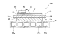
- FIG. 1 shows a power module 100 using a power module substrate 10 according to the present invention.
- the power module 100 is bonded to the power module substrate 10, an electronic component 20 such as a semiconductor chip mounted on the surface of the power module substrate 10, and the surface opposite to the electronic component 20.
- Heat sink 30 is bonded to the power module substrate 10.
- the power module substrate 10 includes a ceramic substrate 11 and metal plates 12 and 13 laminated on both surfaces of the ceramic substrate 11.
- the metal plate 12 laminated on one surface of the ceramic substrate 11 becomes a circuit layer, and the electronic component 20 is soldered to the surface.
- the other metal plate 13 is a heat dissipation layer, and a heat sink 30 is attached to the surface thereof.
- the ceramic substrate 11 is made of AlN (aluminum nitride) and has a thickness of, for example, 635 ⁇ m.
- Both the metal plates 12 and 13 are made of aluminum having a purity of 99% by mass or more. According to JIS standards, aluminum in the 1000s, particularly 1N90 (purity 99.9% by mass or more: so-called 3N aluminum) or 1N99 (purity 99.3%). 99% by mass or more: so-called 4N aluminum) can be used. Aluminum alloys such as JIS A3003 and A6063 can also be used.
- the metal plates 12 and 13 are provided in a rectangular flat plate shape with a side of 30 mm, for example.
- the metal plate 13 serving as a heat dissipation layer is provided with a buffering function against a thermal expansion / contraction difference between the ceramic substrate 11 and the heat sink 30 during thermal cycling. What is formed more thickly is used.
- the thickness of the metal plate 12 is 600 ⁇ m, and the thickness of the metal plate 13 is 1600 ⁇ m.
- highly pure aluminum for example, 1N99 for the metal plate 13 used as a heat radiating layer.
- the brazing material an alloy such as Al—Si, Al—Ge, Al—Cu, Al—Mg, or Al—Mn is used.
- the joint between the metal plates 12 and 13 and the ceramic substrate 11 has a depth of 5 ⁇ m from the joint interface between the metal plate 13 and the ceramic substrate 11 within a region having a width of 200 ⁇ m from the side edge of the metal plates 12 and 13.
- SEM scanning electron microscope
- the total length of the continuous residual oxide present is set to 70% or less with respect to the length of the visual field.
- This continuous residual oxide has a length of 2 ⁇ m or more among the residual oxides existing along the bonding interface, and when there are a plurality of residual oxides having a length of 2 ⁇ m or more in the observation field, Their total length is 70% or less of the length of the observation field. Even if the residual oxide has a length of less than 2 ⁇ m, it is considered continuous if the distance between adjacent residual oxides is 1 ⁇ m or less.
- the shape of the heat sink 30 is not particularly limited.
- the heat sink 30 is formed of a material having good heat conduction, for example, an A3000 aluminum alloy, and has a plurality of flow paths 30a for circulating a cooling medium (for example, cooling water). ing.
- the heat sink 30 and the metal plate 13 serving as the heat dissipation layer of the power module substrate 10 are joined by brazing, and the brazing material may be Al—Si, Al—Ge, Al—Cu, Al—Mg, or An alloy such as Al—Mn is used.
- a plated layer 21 such as Ni—P is formed on the surface of the metal plate 12 serving as a circuit layer, and the electronic component 20 is bonded onto the plated layer.
- a solder material such as Sn—Ag—Cu, Sn—Cu, Sn—Ag, Sn—Sb, Zn—Al, or Pb—Sn is used for joining the electronic component 20.
- Reference numeral 22 in FIG. 1 indicates the solder joint layer.
- the electronic component 20 and the terminal portion of the metal plate 12 are connected by a bonding wire 23 made of aluminum.
- the power module substrate 10 is formed by bonding the ceramic substrate 11 and the metal plates 12 and 13, and then the heat sink 30 is bonded to the metal plate 13.
- the metal plates 12 and 13 are formed from a sheet material by press working.
- the metal plate 12 to be a circuit layer is formed by simply punching from the sheet material.
- the metal plate 13 serving as a heat dissipation layer is stamped from a sheet material.
- Etching is performed by immersing the metal plates 12 and 13 for a predetermined time using a 5% NaOH solution as an etching solution and a temperature of 50 ° C.
- the treatment time is a time during which the surface layer of the metal plates 12 and 13 can be removed by 1.3 ⁇ m or more.
- the etching depth is obtained from the relationship between the specific gravity and the area of the metal plates 12 and 13 by calculating the etching amount based on the difference between the weight before the treatment of the metal plates 12 and 13 and the weight after the treatment.
- the surface of the metal plates 12 and 13 has an oxygen concentration of 1.5 mass analyzed from an oxygen count amount measured with an electron beam microanalyzer (EPMA) at an acceleration voltage of 10 kV, a current of 100 mA, and a beam diameter of 100 ⁇ m.
- the oxide thickness measured by X-ray electron spectroscopy (XPS) in the thickness direction is 35 mm or less.
- the measurement conditions of the X-ray electron spectroscopic analysis are: the output of the X-ray source is 100 W, the path energy is 26 eV, the measurement step is 0.05 eV, the beam diameter is 100 ⁇ m ⁇ 1.4 mm, the detection angle is 90 °, and the detection depth is 80 mm. It is said.
- the surfaces of the metal plates 12 and 13 subjected to the etching treatment have an arithmetic average roughness Ra of 0.05 ⁇ m or more and 0.30 ⁇ m or less, and are formed in an uneven shape.
- the difference between the arithmetic average roughness in the rolling direction and the arithmetic average roughness in the perpendicular direction is 0.10 ⁇ m or less, and the rolling rebar generated during the rolling, etc. Is removed, and the surface roughness has no directivity.
- the ceramic substrate 11 is laminated on the substrate bonding surface 13b of the metal plate 13 via the brazing material, and the other metal plate 12 is laminated on the ceramic substrate 11 via the brazing material.
- the brazing material was pasted by brazing the brazing material foil to the sheet material when the metal plates 12 and 13 were punched from the sheet material by pressing, and the brazing material foil was pasted by punching the brazing material foil together.
- Metal plates 12 and 13 may be formed.
- the laminated ceramic substrate 11 and the metal plates 12 and 13 are brazed by heating in a vacuum atmosphere while pressing in the thickness direction.
- a large number of units composed of the ceramic substrate 11 and the two metal plates 12 and 13 are laminated, and a cushion layer 25 composed of a carbon plate, a graphite plate or the like is provided between the units. These are placed and pressed and heated in a laminated state. At this time, the applied pressure is 0.1 to 2.5 MPa, the heating temperature is 630 to 655 ° C., and the heating time is 1 to 60 minutes. In this brazing process, the brazing material between the ceramic substrate 11 and the metal plates 12 and 13 is melted and fixed together. Thus, the power module substrate 10 is formed by brazing the substrate bonding surface 13b of the metal plate 13 and the ceramic substrate 11.
- the brazing material between the ceramic substrate 11 and the metal plates 12 and 13 is melted to be in a fluid state.
- the surface roughness of the metal plates 12 and 13 is 0.05 ⁇ m or more and 0.30 ⁇ m or less as Ra described above.
- the difference between the arithmetic average roughness in the rolling direction and the arithmetic average roughness in the direction perpendicular thereto is 0.10 ⁇ m or less, so that the molten brazing material is dispersed without being concentrated in one place, and isotropic. To flow.
- the flow of the brazing material follows the rolling bars, and if oxides remain on the surface of the metal plate in such a surface state, the oxides together with the brazing material It will flow and concentrate at the end of the rolling bar.
- the oxides on the surfaces of the metal plates 12 and 13 are reduced, and even if a slight amount of oxide remains, the brazing material is reduced. Since it is dispersed and flows isotropically, the oxide does not concentrate at a specific end. And even if a micro void is attached to this oxide, the micro void is dispersed without concentrating on a specific portion of the joint.
- the metal plate 12 within a range of 200 ⁇ m wide from the side edges of the metal plates 12 and 13 and within a depth of 5 ⁇ m from the bonding interface between the metal plates 12 and 13 and the ceramic substrate 11 is obtained.
- 13 is observed with a scanning electron microscope (SEM) in a field of view with a magnification of 3000 times, the total length of continuous residual oxides continuously present at 2 ⁇ m or more along the bonding interface is the length of the field of view. Is 70% or less.
- the power module substrate 10 is obtained by forming the plating layer 21 of Ni—P or the like on the surface of the metal plate 12 to be the circuit layer.
- the power module substrate 10 and the heat sink 30 are bonded to each other by bonding the metal plate 13 serving as the heat dissipation layer of the power module substrate 10 and the heat sink 30 by a brazing method using a flux (nocolock brazing method).
- a brazing method using a flux (nocolock brazing method).
- a fluoride-based flux that removes oxide on the metal surface is applied to the brazing material surface, and heated to 600 to 615 ° C. in a non-oxidizing atmosphere (for example, N 2 atmosphere) to braze. It is a method to do.
- the brazing material for joining the metal plate 13 and the heat sink 30 is made of, for example, an Ai-Si alloy, and is supplied by being clad in advance on the surface of the heat sink 30 or overlapping the heat sink 30 in the form of a brazing material foil. .
- the power module substrate 10 has a small amount of continuous residual oxide in a region having a predetermined width from the side edge of the joint portion between the ceramic substrate 11 and the metal plate 13 serving as the heat dissipation layer. Does not enter, and the occurrence of peeling can be prevented.
- the power module substrate 10 has the metal plate 13 and the heat sink 30 joined to each other at the joint between the ceramic substrate 11 and the metal plate 13 even when the metal plate 13 and the heat sink 30 are joined by brazing using a flux. Occurrence of peeling of the end portion is prevented, and the power module substrate 10 with high bonding reliability can be obtained.
- a rolled material made of 1N99 aluminum having a thickness of 0.6 mm was punched into 30 mm ⁇ 30 mm, subjected to etching treatment or blast treatment shown in Table 1, and the removal depth of the metal plate surface by the treatment was measured.
- the removal depth was determined by calculating the amount of removal based on the difference between the weight before the treatment of the metal plate and the weight after the treatment, and the relationship with the specific gravity and area of the metal plate.
- an oxygen concentration was analyzed from an oxygen count amount measured with an electron beam microanalyzer (EPMA) at an acceleration voltage of 10 kV, a current of 100 mA, and a beam diameter of 100 ⁇ m, and an X-ray in the thickness direction.
- the oxide thickness was measured by electron spectroscopy (XPS).
- the measurement conditions of the X-ray electron spectroscopic analysis are: the output of the X-ray source is 100 W, the path energy is 26 eV, the measurement step is 0.05 eV, the beam diameter is 100 ⁇ m ⁇ 1.4 mm, the detection angle is 90 °, and the detection depth is 80 mm.
- the thickness was obtained by the above-described equation (1).
- the arithmetic average roughness of the metal plate surface was measured in the rolling direction and the direction perpendicular thereto.
- This metal plate is laminated on both surfaces of a ceramic substrate made of aluminum nitride having a thickness of 0.635 mm through a brazing material foil made of Al-7.5 mass% Si having a thickness of 15 ⁇ m and 30 mm ⁇ 30 mm, and the lamination direction thereof
- the sample was bonded at a temperature of 630 ° C. to 650 ° C. in a vacuum.
- the cross section of the metal plate within a range of 5 ⁇ m from the bonding interface between the ceramic substrate and the metal plate at a portion of 100 ⁇ m to 200 ⁇ m from the side edge of the metal plate Observation was performed with a microscope (SEM) at a field of magnification of 3000 times, and the total length of continuous residual oxides continuously present at 2 ⁇ m or more along the bonding interface was measured.
- SEM used Ultra 55 manufactured by Carl Zeiss under the following conditions.
- Morota Chemical's Nocolok Flux “FL-7” was applied to a heat sink made of A1050 aluminum material with a thickness of 5 mm, and the power was sandwiched between 70 ⁇ m thick brazing foil made of Al-10 mass% Si.
- the metal plates of the module substrate were superposed and joined by heating to 610 ° C. in a nitrogen atmosphere.
- the peeling rate at the bonding interface between the ceramic substrate after bonding and the metal plate bonded to the heat sink, and the peeling rate after the liquid phase thermal cycle test were measured.
- the liquid phase cooling / heating cycle test is a test in which an operation of alternately immersing in a liquid bath at ⁇ 40 ° C. and a liquid bath at 100 ° C. for 10 minutes each is repeated 3000 cycles.
- the initial bonding area is an area to be bonded before bonding, that is, a metal plate area of the heat dissipation layer.
- the edge part peeling part was made into the peeling part which peeling has reached the edge of a metal plate, ie, the peeling part which has an opening part in the edge of a metal plate.
- peeling is indicated by a white portion in the joint, and the area of the edge peeling portion having an opening at the edge of the metal plate was measured in the white portion.
- the peeling length was determined from the peeling length at the center positions of the four sides of the metal plate of the heat dissipation layer after the liquid phase thermal cycle test using an ultrasonic flaw detector. Specifically, as shown in FIG. 4, the lengths S 1 , S 2 and the lengths S 1 , S 2 of each peeling A at the center positions of two opposing sides in the rolling direction (X direction) and the vertical direction (Y direction) of the metal plate S 3 and S 4 were measured, and the average values (S 1 + S 2 ) / 2 and (S 3 + S 4 ) / 2 for each of the X and Y directions were taken. Note that the lengths S 1 to S 4 of the peeling A are the lengths when a perpendicular is drawn to the side closest to the leading edge of the peeling A. These results are shown in Table 1.
- (1) blasting to (2) blasting are as follows.
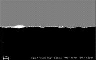
- FIG. 5 is a cross-sectional photograph taken by SEM of Comparative Example 3, in which the lower part of the figure shows a ceramic substrate and the upper part shows a metal plate. In FIG. 4, it can be seen that residual oxides appear in white along the bonding interface on the metal plate side at the bonding interface between the ceramic substrate and the metal plate, and are present in a relatively large length.
- the oxygen concentration analyzed using EPMA is 1.5% by mass or less, and the oxidation measured by XPS analysis. It is effective to use a metal plate having a thickness of 35 mm or less, in which case the oxygen concentration is reliably 1.5% by mass or less by removing the surface of the metal plate to a depth of 1.3 ⁇ m or more, and the oxide thickness. It can be seen that the metal plate can be 35 mm or less.
- the surface roughness of the metal plate is Ra 0.05 ⁇ m to 0.30 ⁇ m, the effect of reducing the peeling rate after the thermal cycle is remarkable, and the difference in surface roughness between the rolling direction and the direction perpendicular thereto is 0. It can be seen that when the thickness is 10 ⁇ m or less, the anisotropy of peeling is reduced, and the effect of reducing the peeling rate is further improved.
- the present invention can be applied to the production of a power module substrate that constitutes a power module that controls a large current and a high voltage, prevents the occurrence of peeling of the end of the metal plate, and improves the bonding reliability.
- a module substrate can be obtained.
Landscapes
- Engineering & Computer Science (AREA)
- Chemical & Material Sciences (AREA)
- Ceramic Engineering (AREA)
- Materials Engineering (AREA)
- Mechanical Engineering (AREA)
- Structural Engineering (AREA)
- Organic Chemistry (AREA)
- Manufacturing & Machinery (AREA)
- Microelectronics & Electronic Packaging (AREA)
- Cooling Or The Like Of Semiconductors Or Solid State Devices (AREA)
- Ceramic Products (AREA)
Abstract
Description
本願は、2012年3月29日に日本国に出願された特願2012-077401号に基づき優先権を主張し、その内容をここに援用する。
特許文献3では、ヒートシンクの天板とパワーモジュール用基板の金属板との接合方法として、フラックスを塗布したろう付け法が記載されている。このろう付け法は、フッ化物系のフラックスをろう材面に塗布してろう材面の酸化物を除去し、非酸化性雰囲気中で加熱して接合するろう付け法であり、高価な設備が不要で、比較的容易に安定したろう付けが可能である。
本発明は、かかる知見の下、以下の解決手段とした。
連続残留酸化物とは、接合界面に沿って存在する残留酸化物のうち、長さが2μm以上有するものとし、2μm以上の長さの残留酸化物が観察視野内に複数存在する場合は、それらの合計の長さが観察視野の長さの70%以下とされる。長さが2μm未満の残留酸化物であっても、隣合う残留酸化物間の距離が1μm以下の場合は連続しているとみなす。
この接合部の端部に連続残留酸化物が観察視野の長さの70%を超えて存在すると、その金属板とヒートシンクとの接合時にセラミックス基板と金属板との接合界面において、金属板の端部で剥離が生じるおそれがある。
セラミックス基板と接合する前の金属板として、その酸素濃度及び酸化物厚さが上記測定値内のものを用いることにより、接合後の連続残留酸化物を低減して微小ボイドの発生を抑制することができる。
金属板の酸化物としては一般には金属板表面に形成される酸化膜が想定される。しかし、この酸化膜を単純に除去するだけでは接合部の残留酸化物は消滅しない。本発明者は、この酸化膜以外に付着する酸化物について調査研究したところ、金属板の圧延時の磨耗粉等が金属板表面に埋まり込んでおり、この磨耗粉等の酸化物が接合部に残留していることを見出した。この磨耗粉等は、金属板表面の酸化膜に比べて粗大であることから、これを除去するためには、表面層を1.3μm以上除去することが必要である。その除去方法としてはエッチング処理が好適であるが、ブラスト処理や、ブラスト処理とエッチング処理とを併用するものであってもよい。
金属板の表面に生じる微細な凹凸により酸化物が分断されるとともに、ろう付け時に溶融したろう材も分断して接合面内を等方的に流動し、その結果、酸化物が特定の端部に集中することが抑制され、2μm以上連続して存在する連続残留酸化物を低減することができる。
本発明の製造方法において、前記算術平均粗さRaは、前記金属板の圧延方向の算術平均粗さとその直角方向の算術平均粗さとの差が0.10μm以下であるとよい。
金属板の表面状態がより等方的になるので、剥離の異方性が低減し、剥離率の低減効果をより向上させることができる。
この場合、金属板12,13とセラミックス基板11との接合部は、金属板12,13の側縁から200μmの幅の領域内で金属板13とセラミックス基板11との接合界面から5μmの深さの範囲内の金属板12,13の断面(上記幅を横断する方向の断面)を走査型電子顕微鏡(SEM)により倍率3000倍の視野で観察した際に、接合界面に沿って2μm以上連続して存在する連続残留酸化物の合計長さが、視野の長さに対して70%以下とされる。
この連続残留酸化物とは、接合界面に沿って存在する残留酸化物のうち、長さが2μm以上有するものとし、2μm以上の長さの残留酸化物が観察視野内に複数存在する場合は、それらの合計の長さが観察視野の長さの70%以下とされる。長さが2μm未満の残留酸化物であっても、隣合う残留酸化物間の距離が1μm以下の場合は連続しているとみなす。
エッチング液として5%NaOH溶液を用い、液温を50℃として金属板12,13を所定時間浸漬することによりエッチング処理する。処理時間は、金属板12,13の表面層を1.3μm以上除去できる時間とする。エッチング深さは、金属板12,13の処理前の重量と処理後の重量との差によりエッチング量を算出し、金属板12,13の比重及び面積との関係で求められる。
このエッチング処理により、金属板12,13の表面は、電子線マイクロアナライザ(EPMA)を用いて加速電圧10kV、電流100mA、ビーム径100μmで測定した酸素カウント量から分析した酸素濃度が1.5質量%以下であり、厚さ方向のX線電子分光分析(XPS)により測定した酸化物厚さが35Å以下となる。
X線電子分光分析の測定条件は、X線源の出力100W、パスエネルギー26eV、測定ステップ0.05eV、分析領域としてビーム径100μm×1.4mm、検出角度90°であり、検出深さが80Åとされる。そして、酸化物厚さは、このX線電子分光分析により得られたスペクトルから酸化物由来の酸化物ピークと母材の金属ピークとを波形分離し、これらのデータ解析により、金属ピークの面積比を次の(1)式に代入することにより得られる。
d=2.68×ln(1/A)×10…(1)
d:酸化物厚さ(Å)
A:金属ピークの面積比
金属板に圧延筋が残っていると、ろう材の流動が圧延筋に沿ったものとなり、そのような表面状態の金属板表面に酸化物が残存していると、その酸化物がろう材とともに流動して圧延筋の端部に集中することになる。これに対して、この実施形態の金属板12,13を用いることにより、金属板12,13表面の酸化物が低減されているとともに、わずかに酸化物が残存していたとしても、ろう材が分散して等方的に流動するため、酸化物が特定の端部に集中することがない。そして、この酸化物に微小ボイドが付属していた場合でも、その微小ボイドが接合部の特定箇所に集中することなく分散する。
このフラックスは、ろう付けの際に金属表面の酸化物を洗い流して清浄化するものであり、このフラックスの侵入を防止するためには、フラックスが反応し易い酸化物が存在しなければよい。このパワーモジュール用基板10は前述したようにセラミックス基板11と放熱層となる金属板13との接合部の側縁から所定幅の領域内の連続残留酸化物が少ないので、この端部からのフラックスが侵入することがなく、剥離の発生を防止することができる。
1N99アルミニウムからなる厚さ0.6mmの圧延材を30mm×30mmに打ち抜き、表1に示すエッチング処理又はブラスト処理を施し、その処理による金属板表面の除去深さを測定した。除去深さは、金属板の処理前の重量と処理後の重量との差により除去量を算出し、金属板の比重及び面積との関係で求めた。
また、表面を処理した金属板について、電子線マイクロアナライザ(EPMA)を用いて加速電圧10kV、電流100mA、ビーム径100μmで測定した酸素カウント量から酸素濃度を分析するとともに、厚さ方向のX線電子分光分析(XPS)により酸化物厚さを測定した。
X線電子分光分析の測定条件は、X線源の出力100W、パスエネルギー26eV、測定ステップ0.05eV、分析領域としてビーム径100μm×1.4mm、検出角度90°であり、検出深さが80Åとされ、前述の(1)式により厚さを求めた。
また、金属板表面の算術平均粗さを圧延方向及びその直角方向でそれぞれ測定した。
得られたパワーモジュール用基板の断面観察により、金属板の側縁から100μm~200μmの部分でセラミックス基板と金属板との接合界面から5μmの深さの範囲内の金属板の断面を走査型電子顕微鏡(SEM)により倍率3000倍の視野で観察し、接合界面に沿って2μm以上連続して存在する連続残留酸化物の合計長さを測定した。
この場合、SEMはCarl Zeiss社製Ultra55を以下の条件で使用した。
観察面:化学研磨による鏡面(蒸着なし)
Signal A:In-lens
Mag:3.00KX
WD:4.0mm
EHT:1kV(加速電圧)
また、長さが2μm未満の残留酸化物であっても、隣合う残留酸化物間の距離が1μm以下の場合は連続しているものとした。
接合後のセラミックス基板とヒートシンクに接合されている金属板との間の接合界面の剥離率と、液相冷熱サイクル試験後の剥離率とを測定した。液相冷熱サイクル試験は、-40℃の液槽と100℃の液槽とにそれぞれ10分ずつ交互に浸漬する操作を3000サイクル繰り返す試験である。
端部剥離率は、超音波探傷装置を用いて接合部を評価し、端部剥離率=端部剥離部の面積/初期接合面積の式から算出した。ここで、初期接合面積とは、接合前における接合すべき面積、すなわち放熱層の金属板面積とした。また、端部剥離部とは、剥離が金属板の端縁にまで至っている剥離部、つまり、金属板の端縁に開口部を有する剥離部とした。超音波探傷像において、剥離は接合部内の白色部で示されることから、この白色部のうち、金属板の端縁に開口部を有する端部剥離部の面積を測定した。
剥がれ長さは、超音波探傷装置を用いて、液相冷熱サイクル試験後における放熱層の金属板の四辺の中心位置における剥がれ長さから求めた。具体的には、図4に示すとおり、金属板の圧延方向(X方向)及びその垂直方向(Y方向)の対向する二辺の中心位置における夫々の剥がれAの長さS1,S2及びS3,S4を測定し、X方向及びY方向ごとの平均値(S1+S2)/2,(S3+S4)/2とした。なお、剥がれAの長さS1~S4は、剥がれAの最先端から最も近い辺に垂線を下ろしたときの長さとした。
これらの結果を表1に示す。

(1)ブラスト:樹脂コートした砥粒による粒度#8000のブラスト処理
(2)ブラスト:樹脂コートした砥粒による粒度#3000のブラスト処理
図5は比較例3のSEMによる断面写真であり、図の下部がセラミックス基板、上部が金属板を示している。この図4では、セラミックス基板と金属板との接合界面における金属板側に接合界面に沿って白く並んで見えるのが残留酸化物であり、比較的大きい長さで存在していることがわかる。
また、金属板の表面粗さがRa0.05μm~0.30μmであると、冷熱サイクル後の剥離率低減効果が顕著であり、さらに圧延方向とその直角方向との表面粗さの差が0.10μm以下であると、剥離の異方性が低減し、剥離率の低減効果がより向上していることがわかる。
11 セラミックス基板
12 金属板
13 金属板
13a ヒートシンク接合面
13b 基板接合面
13c 側面
20 電子部品
21 めっき層
22 はんだ接合層
23 ボンディングワイヤ
25 クッション層
30 ヒートシンク
30a 流路
100 パワーモジュール
T 接合界面
Q 連続残留酸化物
Claims (5)
- セラミックス基板の少なくとも一方の面にアルミニウム又はアルミニウム合金からなる金属板をろう付けにより接合してなり、前記金属板の側縁から200μmの幅の領域内で前記金属板と前記セラミックス基板との接合界面から5μmの深さの範囲内の前記金属板の断面を走査型電子顕微鏡により倍率3000倍の視野で観察した際に、前記接合界面に沿って2μm以上連続して存在する連続残留酸化物の合計長さが、前記視野の長さに対して70%以下であることを特徴とするパワーモジュール用基板。
- セラミックス基板の少なくとも一方の面にアルミニウム又はアルミニウム合金からなる金属板をろう付けにより接合してパワーモジュール用基板を製造する方法であって、前記セラミックス基板と接合する前の金属板として、電子線マイクロアナライザを用いて加速電圧10kV、電流100mA、ビーム径100μmで測定した酸素カウント量から分析
した酸素濃度が1.5質量%以下であり、厚さ方向のX線電子分光分析により測定した酸化物厚さが35Å以下であるものを用いることを特徴とするパワーモジュール用基板の製造方法。 - 前記金属板を前記セラミックス基板に接合する前に、前記金属板の表面層を1.3μm以上除去することを特徴とする請求項2記載のパワーモジュール用基板の製造方法。
- 前記セラミックス基板に接合する前の金属板表面の算術平均粗さRaが0.05μm以上0.30μm以下であることを特徴とする請求項3記載のパワーモジュール用基板の製造方法。
- 前記算術平均粗さRaは、前記金属板の圧延方向の算術平均粗さとその直角方向の算術平均粗さとの差が0.10μm以下であることを特徴とする請求項4記載のパワーモジュール用基板の製造方法。
Priority Applications (5)
| Application Number | Priority Date | Filing Date | Title |
|---|---|---|---|
| IN7986DEN2014 IN2014DN07986A (ja) | 2012-03-29 | 2013-03-27 | |
| US14/388,953 US9862045B2 (en) | 2012-03-29 | 2013-03-27 | Power-module substrate and manufacturing method thereof |
| KR1020147029947A KR102004573B1 (ko) | 2012-03-29 | 2013-03-27 | 파워 모듈용 기판 및 그 제조 방법 |
| EP13768726.5A EP2833397B1 (en) | 2012-03-29 | 2013-03-27 | Substrate for power module and manufacturing method therefor |
| CN201380015335.4A CN104170077B (zh) | 2012-03-29 | 2013-03-27 | 功率模块用基板及其制造方法 |
Applications Claiming Priority (2)
| Application Number | Priority Date | Filing Date | Title |
|---|---|---|---|
| JP2012077401A JP5614423B2 (ja) | 2012-03-29 | 2012-03-29 | パワーモジュール用基板及びその製造方法 |
| JP2012-077401 | 2012-03-29 |
Publications (1)
| Publication Number | Publication Date |
|---|---|
| WO2013146881A1 true WO2013146881A1 (ja) | 2013-10-03 |
Family
ID=49260130
Family Applications (1)
| Application Number | Title | Priority Date | Filing Date |
|---|---|---|---|
| PCT/JP2013/059001 Ceased WO2013146881A1 (ja) | 2012-03-29 | 2013-03-27 | パワーモジュール用基板及びその製造方法 |
Country Status (7)
| Country | Link |
|---|---|
| US (1) | US9862045B2 (ja) |
| EP (1) | EP2833397B1 (ja) |
| JP (1) | JP5614423B2 (ja) |
| KR (1) | KR102004573B1 (ja) |
| CN (1) | CN104170077B (ja) |
| IN (1) | IN2014DN07986A (ja) |
| WO (1) | WO2013146881A1 (ja) |
Cited By (2)
| Publication number | Priority date | Publication date | Assignee | Title |
|---|---|---|---|---|
| US10752973B2 (en) | 2014-10-31 | 2020-08-25 | Nippon Steel & Sumikin Stainless Steel Corporation | Ferrite-based stainless steel with high resistance to corrosiveness caused by exhaust gas and condensation and high brazing properties and method for manufacturing same |
| WO2024195329A1 (ja) * | 2023-03-17 | 2024-09-26 | Dowaメタルテック株式会社 | 銅-セラミックス回路基板およびその製造方法 |
Families Citing this family (7)
| Publication number | Priority date | Publication date | Assignee | Title |
|---|---|---|---|---|
| JP6287216B2 (ja) * | 2014-01-08 | 2018-03-07 | 三菱マテリアル株式会社 | ヒートシンク付パワーモジュール用基板の製造方法 |
| JP6323104B2 (ja) * | 2014-03-25 | 2018-05-16 | 三菱マテリアル株式会社 | ヒートシンク付パワーモジュール用基板の製造方法 |
| JP6287428B2 (ja) * | 2014-03-25 | 2018-03-07 | 三菱マテリアル株式会社 | ヒートシンク付パワーモジュール用基板の製造方法 |
| WO2019003725A1 (ja) * | 2017-06-28 | 2019-01-03 | 京セラ株式会社 | パワーモジュール用基板およびパワーモジュール |
| CN113939095B (zh) * | 2020-06-29 | 2023-02-10 | 比亚迪股份有限公司 | 一种陶瓷覆铜板及其制备方法 |
| CN116368610A (zh) | 2020-10-29 | 2023-06-30 | Ngk电子器件株式会社 | 半导体装置用基板 |
| CN117460174B (zh) * | 2023-12-25 | 2024-04-02 | 广州先艺电子科技有限公司 | 一种图案化amb陶瓷覆铜板的制备方法 |
Citations (5)
| Publication number | Priority date | Publication date | Assignee | Title |
|---|---|---|---|---|
| JP2001121287A (ja) * | 1999-10-21 | 2001-05-08 | Denki Kagaku Kogyo Kk | Al系金属用ろう材とそれを用いたセラミックス回路基板 |
| JP2002009212A (ja) | 2000-06-23 | 2002-01-11 | Denki Kagaku Kogyo Kk | 放熱構造体の製造方法 |
| JP2007311527A (ja) | 2006-05-18 | 2007-11-29 | Mitsubishi Materials Corp | パワーモジュール用基板およびパワーモジュール用基板の製造方法並びにパワーモジュール |
| JP2008117833A (ja) * | 2006-11-01 | 2008-05-22 | Mitsubishi Materials Corp | パワーモジュール用基板及びパワーモジュール用基板の製造方法並びにパワーモジュール |
| JP2009105166A (ja) | 2007-10-22 | 2009-05-14 | Toyota Motor Corp | 半導体モジュールの冷却装置 |
Family Cites Families (10)
| Publication number | Priority date | Publication date | Assignee | Title |
|---|---|---|---|---|
| JPH06302927A (ja) * | 1993-04-15 | 1994-10-28 | Matsushita Electric Ind Co Ltd | セラミック配線基板とその製造方法及び電極ペースト |
| JP3890539B2 (ja) * | 1996-04-12 | 2007-03-07 | Dowaホールディングス株式会社 | セラミックス−金属複合回路基板 |
| JPH11343178A (ja) * | 1998-06-02 | 1999-12-14 | Fuji Electric Co Ltd | 銅板と非酸化物セラミックスとの接合方法 |
| JP2001048671A (ja) * | 1999-08-13 | 2001-02-20 | Dowa Mining Co Ltd | 金属−セラミックス接合基板 |
| CN100583193C (zh) * | 2003-11-28 | 2010-01-20 | 株式会社半导体能源研究所 | 制造显示设备的方法 |
| JP4632116B2 (ja) | 2004-03-05 | 2011-02-16 | 日立金属株式会社 | セラミックス回路基板 |
| JP4918856B2 (ja) * | 2004-04-05 | 2012-04-18 | 三菱マテリアル株式会社 | パワーモジュール用基板及びパワーモジュール |
| KR20110033117A (ko) * | 2008-06-06 | 2011-03-30 | 미쓰비시 마테리알 가부시키가이샤 | 파워 모듈용 기판, 파워 모듈, 및 파워 모듈용 기판의 제조 방법 |
| JP5245989B2 (ja) * | 2009-03-31 | 2013-07-24 | 三菱マテリアル株式会社 | パワーモジュール用基板の製造方法およびヒートシンク付パワーモジュール用基板の製造方法 |
| JP5548722B2 (ja) * | 2012-03-30 | 2014-07-16 | 三菱マテリアル株式会社 | ヒートシンク付パワーモジュール用基板、及び、ヒートシンク付パワーモジュール用基板の製造方法 |
-
2012
- 2012-03-29 JP JP2012077401A patent/JP5614423B2/ja active Active
-
2013
- 2013-03-27 KR KR1020147029947A patent/KR102004573B1/ko not_active Expired - Fee Related
- 2013-03-27 US US14/388,953 patent/US9862045B2/en active Active
- 2013-03-27 WO PCT/JP2013/059001 patent/WO2013146881A1/ja not_active Ceased
- 2013-03-27 CN CN201380015335.4A patent/CN104170077B/zh active Active
- 2013-03-27 EP EP13768726.5A patent/EP2833397B1/en active Active
- 2013-03-27 IN IN7986DEN2014 patent/IN2014DN07986A/en unknown
Patent Citations (5)
| Publication number | Priority date | Publication date | Assignee | Title |
|---|---|---|---|---|
| JP2001121287A (ja) * | 1999-10-21 | 2001-05-08 | Denki Kagaku Kogyo Kk | Al系金属用ろう材とそれを用いたセラミックス回路基板 |
| JP2002009212A (ja) | 2000-06-23 | 2002-01-11 | Denki Kagaku Kogyo Kk | 放熱構造体の製造方法 |
| JP2007311527A (ja) | 2006-05-18 | 2007-11-29 | Mitsubishi Materials Corp | パワーモジュール用基板およびパワーモジュール用基板の製造方法並びにパワーモジュール |
| JP2008117833A (ja) * | 2006-11-01 | 2008-05-22 | Mitsubishi Materials Corp | パワーモジュール用基板及びパワーモジュール用基板の製造方法並びにパワーモジュール |
| JP2009105166A (ja) | 2007-10-22 | 2009-05-14 | Toyota Motor Corp | 半導体モジュールの冷却装置 |
Non-Patent Citations (1)
| Title |
|---|
| See also references of EP2833397A4 |
Cited By (2)
| Publication number | Priority date | Publication date | Assignee | Title |
|---|---|---|---|---|
| US10752973B2 (en) | 2014-10-31 | 2020-08-25 | Nippon Steel & Sumikin Stainless Steel Corporation | Ferrite-based stainless steel with high resistance to corrosiveness caused by exhaust gas and condensation and high brazing properties and method for manufacturing same |
| WO2024195329A1 (ja) * | 2023-03-17 | 2024-09-26 | Dowaメタルテック株式会社 | 銅-セラミックス回路基板およびその製造方法 |
Also Published As
| Publication number | Publication date |
|---|---|
| JP5614423B2 (ja) | 2014-10-29 |
| EP2833397A1 (en) | 2015-02-04 |
| US20150328706A1 (en) | 2015-11-19 |
| IN2014DN07986A (ja) | 2015-05-01 |
| EP2833397B1 (en) | 2021-12-22 |
| JP2013207236A (ja) | 2013-10-07 |
| CN104170077B (zh) | 2017-07-28 |
| US9862045B2 (en) | 2018-01-09 |
| EP2833397A4 (en) | 2015-11-11 |
| KR20140142322A (ko) | 2014-12-11 |
| CN104170077A (zh) | 2014-11-26 |
| KR102004573B1 (ko) | 2019-07-26 |
Similar Documents
| Publication | Publication Date | Title |
|---|---|---|
| JP5614423B2 (ja) | パワーモジュール用基板及びその製造方法 | |
| KR102272865B1 (ko) | 접합체, 히트 싱크가 부착된 파워 모듈용 기판, 히트 싱크, 접합체의 제조 방법, 히트 싱크가 부착된 파워 모듈용 기판의 제조 방법, 및 히트 싱크의 제조 방법 | |
| CN109417056B (zh) | 铜-陶瓷接合体及绝缘电路基板 | |
| US12027434B2 (en) | Bonded body of copper and ceramic, insulating circuit substrate, bonded body of copper and ceramic production method, and insulating circuit substrate production method | |
| JP5725060B2 (ja) | 接合体、パワーモジュール用基板、及びヒートシンク付パワーモジュール用基板 | |
| KR20110015544A (ko) | 파워 모듈용 기판, 파워 모듈, 및 파워 모듈용 기판의 제조 방법 | |
| JP6432465B2 (ja) | 接合体、ヒートシンク付パワーモジュール用基板、ヒートシンク、接合体の製造方法、ヒートシンク付パワーモジュール用基板の製造方法、及び、ヒートシンクの製造方法 | |
| WO2011040044A1 (ja) | 電子機器用放熱板およびその製造方法 | |
| JP6656657B2 (ja) | セラミックス/アルミニウム接合体、パワーモジュール用基板、及び、パワーモジュール | |
| JP5853727B2 (ja) | ヒートシンク付パワーモジュール用基板の製造方法 | |
| JP5725061B2 (ja) | パワーモジュール用基板、及びヒートシンク付パワーモジュール用基板 | |
| JP6432208B2 (ja) | パワーモジュール用基板の製造方法、及び、ヒートシンク付パワーモジュール用基板の製造方法 | |
| KR20120021152A (ko) | 파워 모듈용 기판, 히트 싱크 부착 파워 모듈용 기판, 파워 모듈 및 파워 모듈용 기판의 제조 방법 | |
| JP6028352B2 (ja) | ヒートシンク付パワーモジュール用基板の製造方法 | |
| US20220223492A1 (en) | Copper/ceramic joined body, insulating circuit substrate, copper/ceramic joined body production method, and insulating circuit substrate production method | |
| JP6152626B2 (ja) | パワーモジュール用基板の製造方法 | |
| JP4876719B2 (ja) | パワー素子搭載用ユニットおよびパワー素子搭載用ユニットの製造方法並びにパワーモジュール | |
| JP2009277991A (ja) | パワーモジュール用基板、パワーモジュール及びパワーモジュール用基板の製造方法 | |
| JP5874416B2 (ja) | ヒートシンク付パワーモジュール用基板の製造方法およびパワーモジュール用基板 | |
| JP5966790B2 (ja) | ヒートシンク付パワーモジュール用基板の製造方法 | |
| JP7243165B2 (ja) | 接合体の製造方法、絶縁回路基板の製造方法、セラミックス基板、接合体、及び、絶縁回路基板 | |
| JP2015185707A (ja) | ヒートシンク付パワーモジュール用基板の製造方法 | |
| WO2020096040A1 (ja) | 接合体、ヒートシンク付絶縁回路基板、及び、ヒートシンク |
Legal Events
| Date | Code | Title | Description |
|---|---|---|---|
| 121 | Ep: the epo has been informed by wipo that ep was designated in this application |
Ref document number: 13768726 Country of ref document: EP Kind code of ref document: A1 |
|
| WWE | Wipo information: entry into national phase |
Ref document number: 14388953 Country of ref document: US |
|
| WWE | Wipo information: entry into national phase |
Ref document number: 2013768726 Country of ref document: EP |
|
| ENP | Entry into the national phase |
Ref document number: 20147029947 Country of ref document: KR Kind code of ref document: A |
|
| NENP | Non-entry into the national phase |
Ref country code: DE |