WO2013153802A1 - モーションセンサとそれを用いた電子機器 - Google Patents
モーションセンサとそれを用いた電子機器 Download PDFInfo
- Publication number
- WO2013153802A1 WO2013153802A1 PCT/JP2013/002427 JP2013002427W WO2013153802A1 WO 2013153802 A1 WO2013153802 A1 WO 2013153802A1 JP 2013002427 W JP2013002427 W JP 2013002427W WO 2013153802 A1 WO2013153802 A1 WO 2013153802A1
- Authority
- WO
- WIPO (PCT)
- Prior art keywords
- power supply
- supply terminal
- signal
- motion
- sensor element
- Prior art date
- Legal status (The legal status is an assumption and is not a legal conclusion. Google has not performed a legal analysis and makes no representation as to the accuracy of the status listed.)
- Ceased
Links
Images







Classifications
-
- H—ELECTRICITY
- H04—ELECTRIC COMMUNICATION TECHNIQUE
- H04N—PICTORIAL COMMUNICATION, e.g. TELEVISION
- H04N23/00—Cameras or camera modules comprising electronic image sensors; Control thereof
- H04N23/60—Control of cameras or camera modules
- H04N23/68—Control of cameras or camera modules for stable pick-up of the scene, e.g. compensating for camera body vibrations
- H04N23/681—Motion detection
-
- G—PHYSICS
- G01—MEASURING; TESTING
- G01C—MEASURING DISTANCES, LEVELS OR BEARINGS; SURVEYING; NAVIGATION; GYROSCOPIC INSTRUMENTS; PHOTOGRAMMETRY OR VIDEOGRAMMETRY
- G01C19/00—Gyroscopes; Turn-sensitive devices using vibrating masses; Turn-sensitive devices without moving masses; Measuring angular rate using gyroscopic effects
- G01C19/56—Turn-sensitive devices using vibrating masses, e.g. vibratory angular rate sensors based on Coriolis forces
- G01C19/5607—Turn-sensitive devices using vibrating masses, e.g. vibratory angular rate sensors based on Coriolis forces using vibrating tuning forks
- G01C19/5614—Signal processing
-
- H—ELECTRICITY
- H03—ELECTRONIC CIRCUITRY
- H03F—AMPLIFIERS
- H03F1/00—Details of amplifiers with only discharge tubes, only semiconductor devices or only unspecified devices as amplifying elements
- H03F1/02—Modifications of amplifiers to raise the efficiency, e.g. gliding Class A stages, use of an auxiliary oscillation
- H03F1/0205—Modifications of amplifiers to raise the efficiency, e.g. gliding Class A stages, use of an auxiliary oscillation in transistor amplifiers
- H03F1/0277—Selecting one or more amplifiers from a plurality of amplifiers
-
- H—ELECTRICITY
- H03—ELECTRONIC CIRCUITRY
- H03F—AMPLIFIERS
- H03F3/00—Amplifiers with only discharge tubes or only semiconductor devices as amplifying elements
- H03F3/45—Differential amplifiers
- H03F3/45071—Differential amplifiers with semiconductor devices only
- H03F3/45076—Differential amplifiers with semiconductor devices only characterised by the way of implementation of the active amplifying circuit in the differential amplifier
- H03F3/45179—Differential amplifiers with semiconductor devices only characterised by the way of implementation of the active amplifying circuit in the differential amplifier using MOSFET transistors as the active amplifying circuit
- H03F3/45183—Long tailed pairs
-
- H—ELECTRICITY
- H03—ELECTRONIC CIRCUITRY
- H03F—AMPLIFIERS
- H03F3/00—Amplifiers with only discharge tubes or only semiconductor devices as amplifying elements
- H03F3/72—Gated amplifiers, i.e. amplifiers which are rendered operative or inoperative by means of a control signal
-
- H—ELECTRICITY
- H03—ELECTRONIC CIRCUITRY
- H03F—AMPLIFIERS
- H03F2203/00—Indexing scheme relating to amplifiers with only discharge tubes or only semiconductor devices as amplifying elements covered by H03F3/00
- H03F2203/45—Indexing scheme relating to differential amplifiers
- H03F2203/45454—Indexing scheme relating to differential amplifiers the CSC comprising biasing means controlled by the input signal
-
- H—ELECTRICITY
- H03—ELECTRONIC CIRCUITRY
- H03F—AMPLIFIERS
- H03F2203/00—Indexing scheme relating to amplifiers with only discharge tubes or only semiconductor devices as amplifying elements covered by H03F3/00
- H03F2203/45—Indexing scheme relating to differential amplifiers
- H03F2203/45476—Indexing scheme relating to differential amplifiers the CSC comprising a mirror circuit
-
- H—ELECTRICITY
- H03—ELECTRONIC CIRCUITRY
- H03F—AMPLIFIERS
- H03F2203/00—Indexing scheme relating to amplifiers with only discharge tubes or only semiconductor devices as amplifying elements covered by H03F3/00
- H03F2203/45—Indexing scheme relating to differential amplifiers
- H03F2203/45506—Indexing scheme relating to differential amplifiers the CSC comprising only one switch
-
- H—ELECTRICITY
- H03—ELECTRONIC CIRCUITRY
- H03F—AMPLIFIERS
- H03F2203/00—Indexing scheme relating to amplifiers with only discharge tubes or only semiconductor devices as amplifying elements covered by H03F3/00
- H03F2203/45—Indexing scheme relating to differential amplifiers
- H03F2203/45631—Indexing scheme relating to differential amplifiers the LC comprising one or more capacitors, e.g. coupling capacitors
-
- H—ELECTRICITY
- H03—ELECTRONIC CIRCUITRY
- H03F—AMPLIFIERS
- H03F2203/00—Indexing scheme relating to amplifiers with only discharge tubes or only semiconductor devices as amplifying elements covered by H03F3/00
- H03F2203/45—Indexing scheme relating to differential amplifiers
- H03F2203/45632—Indexing scheme relating to differential amplifiers the LC comprising one or more capacitors coupled to the LC by feedback
-
- H—ELECTRICITY
- H03—ELECTRONIC CIRCUITRY
- H03F—AMPLIFIERS
- H03F2203/00—Indexing scheme relating to amplifiers with only discharge tubes or only semiconductor devices as amplifying elements covered by H03F3/00
- H03F2203/45—Indexing scheme relating to differential amplifiers
- H03F2203/45634—Indexing scheme relating to differential amplifiers the LC comprising one or more switched capacitors
-
- H—ELECTRICITY
- H03—ELECTRONIC CIRCUITRY
- H03F—AMPLIFIERS
- H03F2203/00—Indexing scheme relating to amplifiers with only discharge tubes or only semiconductor devices as amplifying elements covered by H03F3/00
- H03F2203/45—Indexing scheme relating to differential amplifiers
- H03F2203/45674—Indexing scheme relating to differential amplifiers the LC comprising one current mirror
-
- H—ELECTRICITY
- H03—ELECTRONIC CIRCUITRY
- H03F—AMPLIFIERS
- H03F2203/00—Indexing scheme relating to amplifiers with only discharge tubes or only semiconductor devices as amplifying elements covered by H03F3/00
- H03F2203/45—Indexing scheme relating to differential amplifiers
- H03F2203/45692—Indexing scheme relating to differential amplifiers the LC comprising one or more resistors in series with a capacitor coupled to the LC by feedback
-
- H—ELECTRICITY
- H03—ELECTRONIC CIRCUITRY
- H03F—AMPLIFIERS
- H03F2203/00—Indexing scheme relating to amplifiers with only discharge tubes or only semiconductor devices as amplifying elements covered by H03F3/00
- H03F2203/45—Indexing scheme relating to differential amplifiers
- H03F2203/45702—Indexing scheme relating to differential amplifiers the LC comprising two resistors
-
- H—ELECTRICITY
- H03—ELECTRONIC CIRCUITRY
- H03F—AMPLIFIERS
- H03F2203/00—Indexing scheme relating to amplifiers with only discharge tubes or only semiconductor devices as amplifying elements covered by H03F3/00
- H03F2203/45—Indexing scheme relating to differential amplifiers
- H03F2203/45728—Indexing scheme relating to differential amplifiers the LC comprising one switch
-
- H—ELECTRICITY
- H03—ELECTRONIC CIRCUITRY
- H03F—AMPLIFIERS
- H03F2203/00—Indexing scheme relating to amplifiers with only discharge tubes or only semiconductor devices as amplifying elements covered by H03F3/00
- H03F2203/72—Indexing scheme relating to gated amplifiers, i.e. amplifiers which are rendered operative or inoperative by means of a control signal
- H03F2203/7215—Indexing scheme relating to gated amplifiers, i.e. amplifiers which are rendered operative or inoperative by means of a control signal the gated amplifier being switched on or off by a switch at the input of the amplifier
-
- H—ELECTRICITY
- H03—ELECTRONIC CIRCUITRY
- H03F—AMPLIFIERS
- H03F2203/00—Indexing scheme relating to amplifiers with only discharge tubes or only semiconductor devices as amplifying elements covered by H03F3/00
- H03F2203/72—Indexing scheme relating to gated amplifiers, i.e. amplifiers which are rendered operative or inoperative by means of a control signal
- H03F2203/7221—Indexing scheme relating to gated amplifiers, i.e. amplifiers which are rendered operative or inoperative by means of a control signal the gated amplifier being switched on or off by a switch at the output of the amplifier
Definitions
- the present invention relates to a motion sensor that detects a small motion and a large motion, and an electronic device using the motion sensor.
- Patent Document 1 discloses a motion sensor that detects a large motion and a small motion.
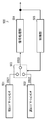
- FIG. 16 is a block diagram of a conventional motion sensor 500 disclosed in Patent Document 1 for detecting a large motion and a small motion.
- the motion sensor 500 includes a low range motion sensor 501 that detects a small acceleration, a high range motion sensor 502 that detects a large acceleration, an output signal S501 of the low range motion sensor 501, and an output signal S502 of the high range motion sensor 502.
- a switching device 503 for switching, a signal processing unit 504 for processing the output signal S503 of the switching device 503, and a control unit 505 for controlling the switching device 503 are provided.
- the control unit 505 normally operates the low range motion sensor 501.
- the control unit 505 operates the high range motion sensor 502 when the acceleration detected by the low range motion sensor 501 exceeds a predetermined threshold.
- the motion sensor includes a sensor element that outputs a sense signal according to the applied motion, and a detection circuit that detects the motion based on the sense signal.
- the detection circuit has a sensor element signal amplifier to which a sense signal is input.
- the sensor element signal amplifier operates so as to be switchable between a normal mode and a low noise mode in which power consumption is larger and noise is smaller than in the normal mode. This motion sensor can detect small motion and large motion with high accuracy.
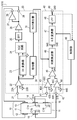
- FIG. 1 is a block diagram of a motion sensor according to Embodiment 1 of the present invention.
- FIG. 2 is a plan view of a sensor element of the motion sensor in the first embodiment.
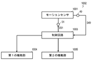
- FIG. 3 is a block diagram of an electronic device using the motion sensor in the first embodiment.
- FIG. 4 is a circuit diagram of a main part of the sensor element signal amplifier of the motion sensor according to the first embodiment.
- FIG. 5 is a circuit diagram of a main part of another sensor element signal amplifier of the motion sensor according to the first embodiment.
- FIG. 6 is a diagram showing noise generated in the sensor element signal amplifier of the motion sensor in the first embodiment.
- FIG. 7 is a circuit diagram of a current source for bias current of the sensor element signal amplifier shown in FIG. FIG.
- FIG. 8 is a circuit diagram of another bias current source for the sensor element signal amplifier shown in FIG.
- FIG. 9 is a block diagram of another motion sensor in the first embodiment.
- FIG. 10 is a block diagram of a motion sensor according to Embodiment 2 of the present invention.
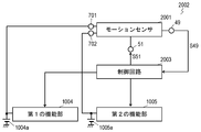
- FIG. 11 is a block diagram of an electronic device using the motion sensor in the second embodiment.
- FIG. 12 is a waveform diagram showing the operation of the motion sensor in the second embodiment.
- FIG. 13 is a block diagram of a motion sensor according to Embodiment 3 of the present invention.
- FIG. 14 is a block diagram of an electronic device using a motion sensor in the third embodiment.
- FIG. 15 is a waveform diagram showing the motion of the motion sensor in the third embodiment.
- FIG. 16 is a block diagram of a conventional motion sensor.
- FIG. 1 is a block diagram of a motion sensor 1001 according to Embodiment 1 of the present invention.
- the motion sensor 1001 includes a sensor element 10, a drive circuit 20 that drives the sensor element 10, a detection circuit 40 that processes a signal output from the sensor element 10 and detects a motion applied to the sensor element 10, and a drive A circuit 20, a detection circuit 40, and a control unit 50 that controls the circuit 20 are provided.
- the motion sensor 1001 according to the first embodiment is an angular velocity sensor that detects an angular velocity that is a motion applied to the sensor element 10.
- FIG. 2 is a plan view of the sensor element 10.
- the sensor element 10 includes a vibrator 11 having a tuning fork shape, drive units 12 and 13, detection units 14 and 15, and a monitor unit 16.
- the drive units 12 and 13, the detection units 14 and 15, and the monitor unit 16 are provided on the vibrator 11.
- the vibrator 11 is formed of a semiconductor substrate such as silicon, or a non-piezoelectric material such as fused quartz or alumina. Since the vibrator 11 is made of silicon, it can be miniaturized using a fine processing technique.
- Each of the drive units 12 and 13, the detection units 14 and 15, and the monitor unit 16 includes a lower electrode provided on the vibrator 11, a piezoelectric material provided on the lower electrode, and an upper provided on the piezoelectric material. Electrode.
- the vibrator 11 is driven to vibrate by a drive signal that is an AC voltage applied to the drive units 12 and 13.
- the frequency of the drive signal is the resonance frequency of the vibrator 11, and the vibrator 11 stably vibrates at the resonance frequency by the drive signal.
- the monitor unit 16 outputs a monitor signal S16 that is a current corresponding to the vibration of the vibrator 11.
- a monitor signal S16 that is a current corresponding to the vibration of the vibrator 11.
- the drive circuit 20 includes a monitor input terminal 21 connected to the monitor unit 16 of the sensor element 10, drive output terminals 28 and 29 connected to the drive units 12 and 13, respectively, and a monitor input terminal. 21, a sensor element signal amplifier 22, a direct current (DC) converter 23, an automatic gain control (AGC) circuit 24, a bandpass filter (BPF) 25, and an output amplifier 26 that amplifies the output of the BPF 25. , An inverting amplifier 27 for inverting the output of the output amplifier 26, a phase shifter 30, a phase corrector 32, and a clock generator 31.
- the sensor element signal amplifier 22 converts the monitor signal S16, which is a current, into a voltage and outputs it.
- the DC converter 23 outputs a DC voltage corresponding to the amplitude of the voltage output from the sensor element signal amplifier 22 and outputs the DC voltage to the AGC circuit 24.
- the AGC circuit 24 amplifies and outputs the voltage output from the sensor element signal amplifier 22 with a gain based on the DC voltage output from the DC converter 23.
- the BPF 25 removes unnecessary frequency components from the voltage output from the AGC circuit 24.
- the output amplifier 26 amplifies the output of the BPF 25 and outputs it as a drive signal to the drive unit 12 of the sensor element 10 through the drive output terminal 28.
- the inverting amplifier 27 inverts the output of the output amplifier 26 and outputs it as a drive signal to the drive unit 13 of the sensor element 10 through the drive output terminal 29.
- the vibrator 11 vibrates by the drive signal output to the drive units 12 and 13.
- the output amplifier 26 drives and vibrates the vibrator 11 based on the monitor signal S16.
- the AGC circuit 24 controls the output to the BPF 25 based on the DC voltage output from the DC converter 23 so that the vibrator 11 vibrates with a constant amplitude.
- the phase shifter 30 shifts the phase of the voltage output from the sensor element signal amplifier 22 by 90 degrees.
- the phase corrector 32 adjusts the phase of the output of the phase shifter 30.
- the clock generator 31 uses the output of the phase corrector 32 to generate a square wave clock signal S31. Thus, the clock generator 31 generates the clock signal S31 according to the output of the phase shifter 30 based on the monitor signal S16.
- the detection circuit 40 has input terminals 41 and 42 connected to the detection units 14 and 15 of the sensor element 10, respectively, and an output terminal 49. Sense signals S14 and S15 output from the detection units 14 and 15 are input to the input terminals 41 and 42, respectively.
- the detection circuit 40 includes a sensor element signal amplifier 43 having an input end 43A connected to the input terminal 41, a sensor element signal amplifier 44 having an input end 44A connected to the input terminal 42, and sensor element signal amplifiers 43, 44.
- a differential amplifier 45 connected to the output terminals 43C and 44C, a synchronous detector 46 connected to the differential amplifier 45, an analog-digital (A / D) converter 47 connected to the synchronous detector 46, A low-pass filter (LPF) 48 connected to the A / D converter 47.
- Input ends 43B and 44B of the sensor element signal amplifiers 43 and 44 are connected to a reference potential 40A.
- the sensor element signal amplifiers 43 and 44 convert the sense signals S14 and S15, which are currents input to the input terminals 43A and 44A, into voltages and output them from the output terminals 43C and 44C.
- the differential amplifier 45 outputs a differential signal S45 which is a difference between voltages output from the output ends 43C and 44C of the sensor element signal amplifiers 43 and 44.
- Each of the sense signals S14 and S15 includes a sense component generated according to an angular velocity that is a motion applied to the sensor element 10, and a vibration component caused by the vibration of the vibrator 11 by the drive signals S12 and S13.
- the sense components of the sense signals S14 and S15 have opposite phases, and the vibration components have the same phase.
- the differential amplifier 45 cancels out the vibration components of the sense signals S14 and S15, and outputs only the sense component as the differential signal S45.
- the synchronous detector 46 synchronously detects the difference signal S45 using the clock signal S31 output from the clock generator 31 and outputs a detection signal S46.
- the sense components of the sense signals S14 and S15 have a phase shifted by 90 degrees with respect to the monitor signal S16 corresponding to the vibration of the vibrator 11.
- the clock signal S31 generated from the monitor signal S16 by the phase shifter 30 and the clock generator 31 has a phase shifted by 90 degrees with respect to the sense component.
- the synchronous detector 46 synchronously detects the difference signal S45 using the clock signal S31, thereby obtaining a detection signal S46 containing only the sense component.
- the A / D converter 47 converts the detection signal S46 into a digital signal, and the low-pass filter 48 outputs from the output terminal 49 a motion signal S49 obtained by removing unnecessary signals from the digital signal.
- the control unit 50 controls the sensor element signal amplifiers 43 and 44 of the detection circuit 40 based on the control signal S51 input to the control terminal 51.
- the control unit 50 further controls the A / D converter 47 and the phase corrector 32 of the drive circuit 20.
- Each of the drive units 12 and 13, the detection units 14 and 15, and the monitor unit 16 constitutes a capacitor composed of an upper electrode and a lower electrode facing each other through a piezoelectric material. That is, as shown in FIG. 1, the detection unit 14, the detection unit 15, and the monitor unit 16 constitute a capacitor C14, a capacitor C15, and a capacitor C16, respectively.
- FIG. 3 is a block diagram of an electronic device 1002 using the motion sensor 1001.
- the electronic device 1002 includes a first function unit 1004 that executes a first function using a small motion, and a second function unit 1005 that executes a second function using a large motion.
- the electronic device 1002 in Embodiment 1 is a portable electronic device having a camera function as a first function and a game machine function and a telephone function as a second function.
- the electronic device 1002 includes a motion sensor 1001, a first function unit 1004 that executes a predetermined first function, and a second function unit 1005 that executes a predetermined second function such as a game machine function and a telephone function.
- the motion sensor 1001 detects the motion, and the output terminal 49 outputs a motion signal S49 corresponding to the motion to the control circuit 1003.
- the control circuit 1003 controls the second function unit 1005 according to the motion signal S49 to cause the second function unit 1005 to execute a game function or a telephone function.
- the motion sensor 1001 detects a motion that is a vibration caused by hand shake, outputs a motion signal S49 corresponding to the motion, and the control circuit 1003 responds to the motion signal S49.
- the influence on the image due to camera shake is canceled by the electronic correction method for correcting the image obtained by the first function unit 1004 or the optical correction method for correcting the lens of the camera.
- the control circuit 1003 outputs to the control terminal 51 of the motion sensor 1001 a control signal S51 indicating which of the first function unit 1004 and the second function unit 1005 is operating.
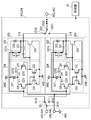
- FIG. 4 is a circuit diagram of a main part of the sensor element signal amplifiers 243 and 244 operating as the sensor element signal amplifiers 43 and 44, and particularly shows a part connected to the input terminals 43A and 44A.
- the differential amplifier circuit 224 and the amplifier circuit 225 constitute a sensor element signal amplifier circuit 253, and the differential amplifier circuit 324 and the amplifier circuit 325 constitute a sensor element signal amplifier circuit 353.
- the switch 251 has a common end 251A connected to the input end 43A (44A) and branch ends 251B and 251C, and selectively connects the common end 251A to the branch ends 251B and 251C.
- the sense signal S14 (S15) is input to the common terminal 251A via the input terminal 43A (44A).
- the differential amplifier circuit 224 includes semiconductor amplifier elements 229 and 231 that are P-channel field effect transistors (hereinafter referred to as FETs), semiconductor amplifier elements 230 and 232 that are N-channel FETs, and a current source 227 for bias current. Is provided.
- One end 227B of the bias current source 227 is connected to the power source 240C.
- the amplifying elements 229 and 230 are directly connected in series between the other end 227A of the bias current source 227 and the reference potential 40B.
- the amplifying elements 231 and 232 are directly connected in series between the end 227A of the bias current source 227 and the reference potential 40B.
- the drain of the amplifying element 229 is connected to the drain of the amplifying element 230.
- the drain of the amplifying element 231 is connected to the drain of the amplifying element 232.
- a connection body having the amplifying elements 229 and 230 connected to each other and a connection body having the amplifying elements 231 and 232 connected to each other are parallel to each other between the end 227A of the bias current source 227 and the reference potential 40B. It is connected.
- the branch end 251 ⁇ / b> B of the switch 251 is connected to the gate of the amplifying element 229.
- the input terminal 43B is connected to the gate of the amplifying element 231.
- Both the gate of the amplifying element 230 and the gate of the amplifying element 232 are connected to the drains of the amplifying elements 229 and 230.
- the drains of the amplification elements 231 and 232 are connected to the amplification circuit 225.
- the amplifier circuit 225 includes a semiconductor amplifier element 234 that is an N-channel FET connected between the current source 233 and the reference potential 40B.
- the drains of the amplification elements 231 and 232 are connected to the gate of the amplification element 234.
- the drain of the amplifying element 234 is connected to the output terminal 218.
- the output terminal 218 is connected to the branch terminal 252B of the switch 252.
- An IV conversion impedance element 237A is connected between the drain of the amplifying element 234 and the gate of the amplifying element 229.
- the IV conversion impedance element 237A includes a resistor connected in series between the gate of the amplification element 229 and the drain of the amplification element 234, and a capacitor connected in parallel with the resistance, and has an impedance.
- the IV conversion impedance element 237A may be composed of other components that constitute impedance instead of the resistor and the capacitor connected in parallel with each other.
- the drain of the amplifying element 234 is connected to the gate of the amplifying element 229 via the IV conversion impedance element 237A to form a feedback loop.
- An oscillation compensation circuit 237 having a time constant is connected between the drain and gate of the amplifying element 234.
- the bias current source 227 supplies bias currents I 229 and I 231 to the sources of the amplifying elements 229 and 231, respectively.
- the oscillation compensation circuit 237 includes a resistor and a capacitor and has a time constant.
- the oscillation compensation circuit 237 is connected in series between the drain and gate of the amplifier element 234.
- the differential amplification circuit 324 includes semiconductor amplification elements 329 and 331 that are P-channel FETs, semiconductor amplification elements 330 and 332 that are N-channel FETs, and a bias current current source 327.
- One end 327B of the bias current source 327 is connected to the power source 340C.
- the amplifying elements 329 and 330 are directly connected in series between the other end 327A of the bias current source 327 and the reference potential 40B.
- the amplifying elements 331 and 332 are directly connected in series between the end 327A of the bias current source 327 and the reference potential 40B.
- the drain of the amplifying element 329 is connected to the drain of the amplifying element 330.
- the drain of the amplifying element 331 is connected to the drain of the amplifying element 332.
- a connection body having the amplifying elements 329 and 330 connected to each other and a connection body having the amplifying elements 331 and 332 connected to each other are parallel to each other between the end 327A of the bias current source 327 and the reference potential 40B. It is connected.
- the branch end 251 ⁇ / b> C of the switch 251 is connected to the gate of the amplifying element 329.
- the input terminal 43B is also connected to the gate of the amplifying element 331.
- Both the gate of the amplification element 330 and the gate of the amplification element 332 are connected to the drains of the amplification elements 329 and 330.
- the drains of the amplification elements 331 and 332 are connected to the amplification circuit 325.
- the amplification circuit 325 includes a semiconductor amplification element 334 that is an N-channel FET connected between the current source 333 and the reference potential 40B.
- the drains of the amplification elements 331 and 332 are connected to the gate of the amplification element 334.
- the drain of the amplifying element 334 is connected to the output terminal 318.
- the output terminal 318 is connected to the branch terminal 252C of the switch 252.
- An IV conversion impedance element 337A is connected between the drain of the amplification element 334 and the gate of the amplification element 329.
- the IV conversion impedance element 337A includes a resistor connected in series between the gate of the amplification element 329 and the drain of the amplification element 334, and a capacitor connected in parallel with the resistance, and has an impedance.
- the IV conversion impedance element 337A may be composed of other components that constitute impedance instead of the resistor and the capacitor connected in parallel with each other.
- the drain of the amplifying element 334 is connected to the gate of the amplifying element 329 via the IV conversion impedance element 337A to form a feedback loop.
- An oscillation compensation circuit 337 having a time constant is connected between the drain and gate of the amplifying element 334.
- the bias current source 327 supplies bias currents I329 and I331 to the sources of the amplifying elements 329 and 331, respectively.
- the oscillation compensation circuit 337 includes a resistor and a capacitor and has a time constant.
- the oscillation compensation circuit 337 is connected in series between the drain and gate of the amplification element 334.
- the current supplied from the bias current source 227 is larger than the bias current source 327. Therefore, the value of the bias current I229 supplied to the amplifier element 229 of the sensor element signal amplifier circuit 253 is larger than the value of the bias current I329 supplied to the amplifier element 329 of the sensor element signal amplifier circuit 353.
- the amplifying elements 229 and 329 mainly generate flicker noise that is inversely proportional to the frequency and thermal noise that does not depend on the frequency.
- the thermal noise generated in the amplifying element 329 becomes larger than the thermal noise generated in the amplifying element 229. Flicker noise does not depend greatly on the bias current.
- the noise generated by the amplifying element 229 is smaller than that of the amplifying element 329, and the power consumption of the amplifying element 229 is larger than that of the amplifying element 329.
- the time constants of the oscillation compensation circuits 237 and 337 are optimally set for the currents of the bias current sources 227 and 327 so that the sensor element signal amplifier circuits 253 and 353 operate stably.
- the switch 251 has a common end 251A connected to the input end 43A (44A) and branch ends 251B and 251C, and selectively connects the common end 251A to the branch ends 251B and 251C.
- the branch ends 251B and 251C are connected to the amplifying elements 229 and 329, respectively.
- the switch 251 selectively outputs a signal input from the input terminal 43A (44A) to the amplifying elements 229 and 329.
- the switch 252 has a common end 252A connected to the output end 43C (44C) and branch ends 252B and 252C, and selectively connects the common end 252A to the branch ends 252B and 252C.
- Branch ends 252B and 252C are connected to output ends 218 and 318, respectively.
- the switch 252 selectively outputs signals output from the output terminals 218 and 318 to the common terminal 252A.
- control unit 50 When the control signal S51 indicates that the control circuit 1003 of the electronic device 1002 operates the second function unit 1005, the control unit 50 selectively connects the common end 251A of the switch 251 to the branch end 251C. Thus, the common end 251A is separated from the branch end 251B. At the same time, the controller 50 selectively connects the common end 252A of the switch 252 to the branch end 252C and separates the common end 252A from the branch end 252B. Thereby, the sense signal S14 (S15) input from the input terminal 43A (44A) is input to the amplification element 329 of the differential amplification circuit 324 of the sensor element signal amplification circuit 353.
- the sense signal S14 is amplified by the differential amplifier circuit 324 and the amplifier circuit 325, output from the output terminal 318, input to the branch terminal 252C of the switch 252, and output from the common terminal 252A.
- a signal output from the common terminal 252A of the switch 252 is output as a voltage from the output terminal 43C (44C) through an amplifier circuit such as an operational amplifier.
- the control unit 50 may turn on the power supply 340C of the sensor element signal amplification circuit 353 and turn off the power supply 240C of the sensor element signal amplification circuit 253. Thereby, the power consumption of the sensor element signal amplifiers 243 and 244 can be reduced.
- the motion sensor 1001 detects a motion having a large amplitude intentionally added by the user.
- control unit 50 When the control signal S51 indicates that the control circuit 1003 operates the first functional unit 1004, the control unit 50 selectively connects the common end 251A of the switch 251 to the branch end 251B, and the common end 251A is moved away from the branch end 251C. At the same time, the controller 50 selectively connects the common end 252A of the switch 252 to the branch end 252B and separates the common end 252A from the branch end 252C.
- the sense signal S14 (S15) input from the input terminal 43A (44A) is input to the amplification element 229 of the differential amplification circuit 224 of the sensor element signal amplification circuit 253.
- the sense signal S14 is amplified by the differential amplifier circuit 224 and the amplifier circuit 225, output from the output terminal 218, input to the branch terminal 252B of the switch 252, and output from the common terminal 252A.
- a signal output from the common terminal 252A of the switch 252 is output as a voltage from the output terminal 43C (44C) through an amplifier circuit such as an operational amplifier.
- the controller 50 may turn on the power supply 240C of the sensor element signal amplification circuit 253 and turn off the power supply 340C of the sensor element signal amplification circuit 353. Thereby, the power consumption of the sensor element signal amplifiers 243 and 244 can be reduced.
- the motion sensor 1001 detects a motion having a small amplitude due to a user's hand shake.
- the noise generated by the amplification element 229 is smaller than that of the amplification element 329, and the power consumption of the amplification element 229 is larger than that of the amplification element 329. Therefore, the motion sensor 1001 can detect a small motion due to camera shake with high accuracy. Further, when a large motion is detected, the noise generated in the differential amplifier circuit 324 is large, but the influence on the detection of the large motion is small. Moreover, since the bias current I329 is small, the motion sensor 1001 operates with a small current consumption.
- a conventional motion sensor 500 shown in FIG. 16 uses two sensor elements, a low-range motion sensor 501 and a high-range motion sensor 502, and it is difficult to reduce the size and cost.
- the switches 251 and 252 are changed as described above according to the magnitude of the motion to be detected, so that the single sensor element 10 can be used to detect small motion with high accuracy. It is possible to achieve both low current consumption when detecting a large motion.
- the current value of the current source 233 may be larger than the current value of the current source 333.
- noise generated in the amplifying element 234 is further smaller than noise generated in the amplifying element 234, and power consumption in the amplifying element 234 is greater than power consumption in the amplifying element 334. Therefore, it is possible to achieve both high-precision detection of small motions and low current consumption when detecting large motions.
- the magnitude of the impedance of the IV conversion impedance element 337A may be larger than that of the IV conversion impedance element 237A.
- the S / N ratio in the IV conversion impedance element 337A of the sensor element signal amplification circuit 353 operating in the normal mode mode is compared with the IV conversion impedance element 237A of the sensor element signal amplification circuit 253 operating in the low mode mode.
- the S / N ratio can be increased, and the motion sensor 1001 can detect a small motion with high accuracy.
- the sensor element signal amplifier 243 (244) operates so as to be switchable between the normal mode and the low noise mode in which power consumption is larger and noise is smaller than in the normal mode.
- the amplifying element 229 has higher power consumption and less noise than the amplifying element 329.
- the sensor element signal amplifiers 243 and 244 operate in the low noise mode by connecting the common end 251A of the switch 251 to the branch end 251C and away from the branch end 251B.
- the normal mode and the low noise mode can be switched from outside the motion sensor 1001.
- the control unit 50 similarly controls the offset and gain of the phase corrector 32 and the A / D converter 47 shown in FIG. As a result, the motion can be detected with high accuracy regardless of the magnitude of the motion.
- the sensor element signal amplifier 22 to which the monitor signal S16 is input may be configured by the same circuit as the sensor element signal amplifiers 243 and 244 shown in FIG.
- FIG. 5 is a circuit diagram of a main part of other sensor element signal amplifiers 143 and 144 that operate as the sensor element signal amplifiers 43 and 44 of the motion sensor 1001 according to the first embodiment, and is particularly connected to the input terminals 43A and 44A.
- the part which is present is shown. 5, the same reference numerals are assigned to the same portions as the sensor element signal amplifiers 243 and 244 shown in FIG.
- the sensor element signal amplifiers 143 and 144 include a differential amplifier circuit 124 and an amplifier circuit 125 instead of the differential amplifier circuits 224 and 324 and the amplifier circuits 225 and 325 included in the sensor element signal amplifiers 243 and 244.
- the switches 251 and 252 are not provided.
- the sensor element signal amplifiers 143 and 144 include a differential amplifier circuit 124 that amplifies a voltage difference between the input terminals 43A and 43B, and an amplifier circuit 125 that amplifies the output of the differential amplifier circuit 124.
- the differential amplifier circuit 124 includes semiconductor amplification elements 129 and 131 that are P-channel field effect transistors (hereinafter referred to as FETs), semiconductor amplification elements 130 and 132 that are N-channel FETs, and a bias current source 127. Is provided. One end 127B of the bias current source 127 is connected to the power source 40C.
- the amplifying elements 129 and 130 are directly connected in series between the other end 127A of the bias current source 127 and the reference potential 40B.
- the amplifying elements 131 and 132 are directly connected in series between the end 127A of the bias current source 127 and the reference potential 40B.
- the drain of the amplifying element 129 is connected to the drain of the amplifying element 130.
- the drain of the amplifying element 131 is connected to the drain of the amplifying element 132.
- a connecting body having the amplifying elements 129 and 130 connected to each other and a connecting body having the amplifying elements 131 and 132 connected to each other are parallel to each other between the end 127A of the bias current source 127 and the reference potential 40B. It is connected.
- the input terminal 43A is connected to the gate of the amplifying element 129.
- the input terminal 43B is connected to the gate of the amplifying element 131.
- Both the gate of the amplifying element 130 and the gate of the amplifying element 132 are connected to the drains of the amplifying elements 129 and 130.
- the drains of the amplification elements 131 and 132 are connected to the amplification circuit 125.
- the amplifying circuit 125 includes a semiconductor amplifying element 134 that is an N-channel FET connected between the current source 133 and the reference potential 40B.
- the drains of the amplifying elements 131 and 132 are connected to the gate of the amplifying element 134.
- the drain of the amplifying element 134 is connected to the output end 118.
- a signal output from the output terminal 118 of the amplifier circuit 125 is output as a voltage from the output terminal 43C (44C) through an amplifier circuit such as an operational amplifier.
- An IV conversion impedance element 137 ⁇ / b> A is connected between the drain of the amplification element 134 and the gate of the amplification element 129.
- the IV conversion impedance element 137A includes a resistor 137B connected in series between the gate of the amplifier element 129 and the drain of the amplifier element 134, and a capacitor 137C connected in parallel with the resistor 137B.
- the IV conversion impedance element 137A may be composed of other components that constitute impedance, instead of the resistor 137B and the capacitor 137C connected in parallel to each other.
- the drain of the amplifying element 134 is connected to the gate of the amplifying element 129 via the IV conversion impedance element 137A to form a feedback loop.
- An oscillation compensation circuit 137 having a time constant is connected between the drain and gate of the amplifying element 134.
- the bias current source 127 supplies bias currents I129 and I131 to the sources of the amplifying elements 129 and 131, respectively.
- the values of the bias currents I129 and I131 can be switched.
- the controller 50 can change the value of the current output from the bias current source 127.
- the sensor element signal amplifiers 143 and 144 operate so as to be switchable between a normal mode and a low noise mode in which power consumption is larger and noise is smaller than in the normal mode.
- the oscillation compensation circuit 137 includes resistors 138 and 141, capacitors 139 and 142, and a switch 140.
- the resistor 138, the capacitor 139, and the switch 140 are connected in series between the source and gate of the amplifying element 134.
- the resistor 141 and the capacitor 142 are connected in series between the source and gate of the amplifying element 134.
- the control circuit 1003 of the electronic device 1002 outputs a control signal S51 to the control unit 50 via the control terminal 51 of the motion sensor 1001.
- the control unit 50 controls the drive circuit 20 and the detection circuit 40 according to the control signal S51.
- control unit 50 sets the current value of the bias current source 127 of the differential amplifier circuit 124 to a predetermined value. I1 is set, and the switch 140 of the oscillation compensation circuit 137 is turned on.
- the motion sensor 1001 detects a motion having a large amplitude intentionally added by the user.
- the control unit 50 sets the current value of the bias current source 127 of the differential amplifier circuit 124 to the predetermined value. Is set to a predetermined value I2 larger than the value I1, and the switch 140 of the oscillation compensation circuit 137 is turned off.
- the motion sensor 1001 detects a motion having a small amplitude, which is a vibration caused by hand shake. Further, the control unit 50 changes the time constant of the oscillation compensation circuit 137 by switching the switch 140 of the oscillation compensation circuit 137 according to the magnitude of the motion.
- the motion applied to the motion sensor 1001 due to hand movement when the first function unit 1004 is operating is the intention of the user when the second function unit 1005 is operated. It has a much smaller amplitude than the motion.
- the first function unit 1004 corrects image data based on the detected camera shake, or mechanically corrects a lens connecting the image to the image sensor of the first function unit 1004 and the image sensor itself, thereby causing an image due to camera shake. Eliminate blurring.
- the motion sensor 1001 needs to detect a motion having a small amplitude due to camera shake with high accuracy.
- the sense signals S14 and S15 output from the detection units 14 and 15 of the sensor element 10 are very weak.
- FIG. 6 shows noise generated in the sensor element signal amplifiers 143 and 144.
- the horizontal axis indicates the frequency on a logarithmic scale
- the vertical axis indicates the noise power on a logarithmic scale.
- the differential amplifier circuit 124 mainly generates flicker noise NF that is inversely proportional to the frequency and thermal noise NT1 that is not dependent on the frequency.
- the differential amplifier circuit 124 generates flicker noise NF and frequency-independent thermal noise NT2.
- the motion sensor 1001 In both cases, the power of the flicker noise NF does not change, but the thermal noise NT2 is smaller than the thermal noise NT1. That is, in the motion sensor 1001, the noise generated in the differential amplifier circuit 124 when detecting a motion with small hand shake is smaller than the noise generated in the differential amplifier circuit 124 when detecting a large motion. Therefore, the motion sensor 1001 can detect a small motion due to camera shake with high accuracy. When a large motion is detected, the noise generated in the differential amplifier circuit 124 is large, but does not affect the detection of the large motion. Moreover, since the current value I1 is small, the motion sensor 1001 operates with a small current consumption.
- the motion sensor 1001 changes the value of the current of the bias current source 127 according to the magnitude of the motion to be detected as described above, thereby enabling high-precision detection of small motion in the low noise mode. It is possible to achieve both a low current consumption when detecting a large motion in the normal mode.
- the bias current source 127 has the sensor element signal amplifiers 143 and 144 in the normal mode as compared with the values of the bias currents I129 and I131 when the sensor element signal amplifiers 143 and 144 operate in the normal mode.
- the bias currents I129 and I131 are increased so as to increase the value during the operation.
- the normal mode and the low noise mode can be switched from outside the motion sensor 1001.
- control unit 50 changes the time constant of the oscillation compensation circuit 137 according to the magnitude of the motion, so that the time constant can be made optimal for the current value of the bias current source 127, and the sensor element can be stably provided.
- the signal amplifiers 143 and 144 can be operated.
- FIG. 7 is a circuit diagram of the current source 127 for bias current.
- the bias current source 127 includes P-channel FETs 151 and 152 and a variable current source 153.
- the gate of the FET 151 and the gate of the FET 152 are connected to the drain of the FET 151, and the sources of the FETs 151 and 152 are connected to the power source 40C to form a current mirror.
- the drain of the FET 151 is connected to the variable current source 153.
- the drain of the FET 152 is an end 127A.
- the variable current source 153 is controlled by the control unit 50 to change the value of the output current.
- the control unit 50 can change the value of the current flowing from the end 127 ⁇ / b> A of the bias current source 127 by changing the value of the current of the variable current source 153.
- FIG. 8 is a circuit diagram of another current source 160 for bias current that operates as the current source 127 for bias current.
- the bias current source 160 includes P-channel FETs 161, 162, 164, a constant current source 163, and a switch 165.
- the gates of the FETs 161, 162, and 164 are connected to the drain of the FET 161, and the sources of the FETs 161, 162, and 164 are connected to the power supply 40C to form a current mirror.
- the constant current source 163 is connected to the drain of the FET 161.
- the drain of the FET 162 is an end 127A.
- the switch 165 is connected between the drain of the FET 162 and the drain of the FET 164.
- the control unit 50 can change the mirror ratio of the current mirror by controlling the switch 165 to intermittently connect the drain of the FET 162 and the drain of the FET 164. That is, when the control unit 50 turns off the switch 165 and disconnects the drain of the FET 162 from the drain of the FET 164, a current having the same value as the current of the constant current source 163 flows from the drain of the FET 162. When the control unit 50 turns on the switch 165 and connects the drain of the FET 162 to the drain of the FET 164, a current twice as large as the current of the constant current source 163 flows from the drain of the FET 162. Thus, the value of the current flowing from the end 127A of the bias current source 160 can be changed by the control unit 50 turning the switch 165 on and off.
- the monitor signal S16 output from the monitor unit 16 is input to the sensor element signal amplifier 22.
- the sensor element signal amplifier 22 can be configured by a circuit in which the bias current current source 127 of the sensor element signal amplifiers 143 and 144 shown in FIG. 5 is replaced with a constant current source.
- the phase corrector 32 shifts the phase of the output of the phase shifter 30.
- the controller 50 changes the value of the current of the bias current source 127 according to the magnitude of the motion, the phase of the output of the sensor element signal amplifiers 143 and 144 changes.
- the controller 50 Based on the control signal S51, the controller 50 adjusts the amount by which the phase corrector 32 shifts the phase according to the magnitude of the motion, that is, according to the current value of the bias current source 127.
- the clock generator 31 changes the phase of the clock signal S31 between when the sensor element signal amplifiers 143 and 144 operate in the normal mode and when in the low noise mode.
- the synchronous detector 46 can obtain the detection signal S46 containing only the sense component with high accuracy.
- the control unit 50 may change the current value of the bias current source 127 of the sensor element signal amplifiers 143 and 144 according to the magnitude of the motion, and may change the offset and gain of the A / D converter 47. .
- motion can be detected with high accuracy regardless of the current value of the bias current source 127 of the sensor element signal amplifiers 143 and 144.
- control unit 50 may change the current value of the current source 133 of the sensor element signal amplifiers 143 and 144 according to the magnitude of the motion.
- the amplifying element 134 affects the noise generated in the sensor element signal amplifiers 143 and 144, though not as much as the amplifying elements 129 to 132.
- the control unit 50 sets the current of the current source 133 to a predetermined value in the normal mode, and sets the current value of the current source 133 larger than the predetermined value in the low noise mode. Set to value.
- noise generated in the amplifying element 134 is smaller than in the normal mode, and power consumption in the amplifying element 134 is increased. Therefore, it is possible to achieve both high-precision detection of small motions and low current consumption when detecting large motions.
- control unit 50 may change the magnitude of the impedance of the IV conversion impedance element 137A of the sensor element signal amplifiers 143 and 144 according to the magnitude of the motion.
- the control unit 50 sets the magnitude of the impedance of the IV conversion impedance element 137A to a predetermined value in the normal mode, and sets the magnitude of the impedance to a value larger than the predetermined value in the low noise mode.
- the signal / noise (S / N) ratio which is the ratio of the signal to the noise in the IV conversion impedance element 137A, can be increased compared to the normal mode, and the motion sensor 1001 can perform small motion with high accuracy. Can be detected.
- the sensor element signal amplifier 22 to which the monitor signal S16 is input may be configured by the same circuit as the sensor element signal amplifiers 143 and 144 shown in FIG.
- the control unit 50 changes the current value of the current source 127 for the bias current of the sensor element signal amplifiers 143 and 144 according to the magnitude of the motion, and changes the current value of the current source 127 for the bias current of the sensor element signal amplifier 22. You can change it.
- the area of the monitor unit 16 is smaller than the detection units 14 and 15. Therefore, the capacity of the capacitor C16 formed by the monitor unit 16 is smaller than the capacitors C14 and C15 formed by the detection units 14 and 15.
- the capacitance of the capacitor C16 can be made the same as that of the capacitors C14 and C15 by adjusting the area of the upper electrode and the thickness of the piezoelectric material.
- the control unit 50 changes the current value of the bias current current source 127 of the sensor element signal amplifier 22 in the same manner as the current value of the bias current current source 127 of the sensor element signal amplifiers 143 and 144.
- the phase corrector 32 can be eliminated. That is, in this case, the control unit 50 does not need to adjust the phase of the clock signal S31 supplied to the synchronous detector 46 even if the current of the bias current source 127 of the sensor element signal amplifiers 143 and 144 is changed. .
- the sensor element signal amplifier 243 (244) shown in FIG. 4 includes two differential amplifier circuits 224 and 324 and two amplifier circuits 225 and 325.
- the sensor element signal amplifier 143 (144) shown in FIG. 5 includes only one differential amplifier circuit 124 and one amplifier circuit 125, the sensor element signal amplifier 243 (244) shown in FIG. Therefore, the circuit scale can be reduced, and the motion sensor 1001 can be downsized.
- FIG. 9 is a block diagram of another motion sensor 1010 according to the first embodiment. 9, the same reference numerals are assigned to the same parts as those of the motion sensor 1001 shown in FIGS.
- a motion sensor 1010 illustrated in FIG. 9 includes a control unit 60 instead of the control unit 50.
- the control unit 60 does not have the control terminal 51 to which the control signal S51 is input.
- the control unit 50 of the motion sensor 1001 illustrated in FIG. 1 includes the electronic device 1002 illustrated in FIG.
- the switches 252 and 253 may be switched in accordance with the control signal S51 sent from the control circuit 1003.
- the sensor element signal amplifier 22 operates in a switchable manner between a normal mode and a low noise mode that consumes more power and has less noise than the normal mode.
- the control unit 60 of the sensor 1010 switches the switches 252 and 253 according to the detected magnitude of motion. Thereby, the motion sensor 1010 operates in an optimum state with respect to the magnitude of the motion without an external control signal.
- the control unit 50 of the motion sensor 1001 illustrated in FIG. 1 includes the electronic device 1002 illustrated in FIG.
- the current value of the bias current current source 127 of the sensor element signal amplifiers 143 and 144 is changed, and further the current of the bias current current source 127 of the sensor element signal amplifier 22 is changed.
- the value of may be changed.
- the sensor element signal amplifier 22 operates in a switchable manner between a normal mode and a low noise mode that consumes more power and has less noise than the normal mode.
- the control unit 60 of the sensor 1010 determines the current value of the bias current current source 127 of the sensor element signal amplifiers 143 and 144 and the bias current current source 127 of the sensor element signal amplifier 22 according to the magnitude of the detected motion. Change the current value. Thereby, the motion sensor 1010 operates in an optimum state with respect to the magnitude of the motion without an external control signal.
- control unit 50 of the motion sensor 1001 shown in FIG. 1 adds the current of the bias current source 127 according to the magnitude of the detected motion in addition to the control signal S51 in the same manner as the control unit 60 shown in FIG. You may change the size of. Accordingly, in the electronic device 1002 illustrated in FIG. 3, the control circuit 1003 can operate the second functional unit 1005 with high accuracy even when operating the second functional unit 1005 or in response to a small motion.
- the first function unit 1004 functions as a camera as the predetermined first function, and the motion sensors 1001 and 1010 detect small motion due to camera shake.
- the predetermined first function may be another function such as a game function controlled by a small motion.
- the motion sensors 1001 and 1010 in the first embodiment include the sensor element 10 that detects the angular velocity and detects the angular velocity.
- the motion sensors 1001 and 1010 according to Embodiment 1 may detect motion other than angular velocity such as acceleration and velocity.
- FIG. 10 is a block diagram of the motion sensor 2001 according to Embodiment 2 of the present invention. 10, the same reference numerals are assigned to the same parts as those of the motion sensor 1001 in the first embodiment shown in FIG.
- the motion sensor 2001 is a detection circuit that detects a motion applied to the sensor element 10 by processing a signal output from the sensor element 10 instead of the detection circuit 40 of the motion sensor 1001 in the first embodiment shown in FIG. 2040. Similar to the motion sensor 1001 in the first embodiment, the motion sensor 2001 in the second embodiment is a motion sensor that detects an angular velocity that is a motion applied to the sensor element 10.
- the detection circuit 2040 further includes a masking unit 47a connected to the analog / digital (A / D) converter 47 in the detection circuit 40 according to the first embodiment shown in FIG.
- the low-pass filter (LPF) 48 is connected to the masking unit 47a, and is connected to the A / D converter 47 via the masking unit 47a.
- the control signal S705a is input to the masking unit 47a, and the masking unit 47a masks and outputs the digital signal according to the control signal S705a.
- the low-pass filter 48 outputs from the output terminal 49 a motion signal S49 obtained by removing unnecessary signals from the digital signal output from the masking unit 47a.
- FIG. 11 is a block diagram of an electronic device 2002 using the motion sensor 2001. 11, the same reference numerals are assigned to the same portions as those of electronic device 1002 in the first embodiment shown in FIG.
- the electronic device 2002 in the second embodiment includes a control circuit 2003 and a motion sensor 2001 shown in FIG. 10 instead of the control circuit 1003 and the motion sensor 1001 of the electronic device 1002 in the first embodiment shown in FIG.
- the electronic device 2002 includes a first external power source 1004a that is provided in the first function unit 1004, supplies power to the first function unit 1004, and operates the first function unit 1004, and a second function.
- a second external power source 1005a that is provided in the unit 1005 and supplies power to the second functional unit 1005 to operate the second functional unit 1005.
- the external power supplies 1004a and 1005a supply voltages E4 and E5 to the function units 1004 and 1005, respectively.
- the control circuit 2003 sets the voltage E4 of the first external power supply 1004a to the voltage V4 when operating the first function unit 1004.
- the voltage of the second external power supply 1005a is set to zero.
- the control circuit 2003 sets the voltage E5 of the second external power supply 1005a to the voltage V5 when the second function unit 1005 is operating, and sets the voltage of the first external power supply 1004a to zero.
- the voltages V4 and V5 are 2.4 (V) and 3.6 (V), respectively.
- the motion sensor 2001 includes a first power supply terminal 701 configured to be connected to a first external power supply 1004a and a second external power supply 1005a.
- a second power supply terminal 702 configured to be connected, a switch 703, a first comparator 704, a second comparator 706, a switching control unit 705, a low-pass filter 707, and a low loss (LDO) regulator 707a.
- power is supplied to the motion sensor 1001 from the external power sources 1004a and 1005a that supply power to the function units 1004 and 1005, respectively.
- the switch 703 is either the voltage E4 (voltage V4) of the first external power supply 1004a input from the first power supply terminal 701 or the voltage E5 (V5) of the external power supply 1005a input from the second power supply terminal 702.
- the voltage E703 obtained by selecting one is supplied to the drive circuit 20 and the detection circuit 2040 and loaded.
- the first comparator 704 determines the voltage E4 of the first power supply terminal 701 with a predetermined threshold value, and outputs a high level or low level signal to the switching control unit 705. That is, the first comparator 704 outputs a high level signal to the switching control unit 705 when the voltage E4 is equal to or higher than the predetermined threshold, and when the voltage E4 is lower than the predetermined threshold.
- a low level signal is output to the switching control unit 705.
- the second comparator 706 determines the voltage E5 of the second power supply terminal 702 based on the predetermined threshold value, and outputs a high level or low level signal to the switching control unit 705. That is, the second comparator 706 outputs a high level signal to the switching control unit 705 when the voltage E5 is equal to or higher than the predetermined threshold, and when the voltage E5 is lower than the predetermined threshold.
- a low level signal is output to the switching control unit 705.
- the switch 703 is connected to the first power supply terminal 701 and the first power supply terminal 701 based on the signal output from the switching control unit 705, that is, based on the determination result of the first comparator 704 and the determination result of the second comparator 706.
- the masking unit 47a of the detection circuit 2040 masks the signal output from the A / D converter 47 over a predetermined time from when the switch 703 switches between the first power supply terminal 701 and the second power supply terminal 702.
- the predetermined time is about 1 msec.
- a low-pass filter 707 for cutting noise is connected to the output terminal of the switch 703. The low-pass filter 707 generates a transient response of the signal output from the A / D converter 47 with respect to switching of the switch 703.
- FIG. 12 shows changes with time of the voltage E4 of the first external power supply 1004a, the voltage E5 of the second external power supply 1005a, and the voltage E707 output from the low-pass filter 707.
- the control circuit 2003 selects and operates both the first functional unit 1004 and the second functional unit 1005.
- the voltage E4 of the first external power supply 1004a becomes the voltage V4 to operate the first functional unit 1004
- the second In order to operate the functional unit 1005 becomes the voltage V5.
- the comparators 704 and 706 determine the voltages E4 and E5 and output a high level signal to the switching control unit 705.
- the switch 703 is based on the determination results of the comparators 704 and 706.
- the voltage E5 of the second external power supply 1005a is selected and output to the low-pass filter 707 in preference to the voltage E4 of the first external power supply 1004a.
- the control circuit 2003 stops the operation of the second functional unit 1005 at the time tp1, and the control circuit 2003 operates the second functional unit 1005 in the period P2 from the time tp1 to tp2. Only the first function unit 1004 is operated.
- the voltage E5 of the second external power supply 1005a supplied to the second power supply terminal 702 becomes zero.
- the first comparator 704 continues to output a high level signal to the switching control unit 705, while the second comparator 706 outputs a low level signal to the switching control unit 705.
- a low level signal from the second comparator 706 is input to the masking unit 47 a in the detection circuit 2040 via the switching control unit 705.
- the masking unit 47a masks the signal output from the A / D converter 47 for a predetermined time TW1 from the time point tp1, and outputs a constant value signal to the LPF 48 regardless of the change in the voltage E707.
- the voltage E707 is settled at the voltage E4 supplied to the first power supply terminal 701.
- the predetermined time TW1 is about 1 msec.
- the masking unit 47a inputs the signal output from the A / D converter 47 to the LPF 48 without masking.
- the detection circuit 2040 can output a signal corresponding to the motion from the output terminal 49 without being affected by the fluctuation of the voltage E707.
- the output signal from the detection circuit 2040 varies over a predetermined time (1 msec in the second embodiment) when switching the switch 703 by the masking unit 47a of the detection circuit 2040. I won't let you. Therefore, even if the output signal is going to fluctuate due to a transient response at the time of switching of the switch 703, the output signal can be prevented from fluctuating over the predetermined time by the masking unit 47a, thereby stabilizing the output signal.
- the voltage E5 supplied to the second power supply terminal 702 is changed from zero to the voltage V5 (3.6 V in the second embodiment). It becomes. That is, a high level signal is continuously output from the first comparator 704 to the switching control unit 705, and a high level signal is output from the second comparator 706 to the switching control unit 705. Thereby, in the period P3 after the time tp2, the switch 703 outputs the voltage E5 (V5) supplied to the second power supply terminal 702. At time tp2, the voltage E707 output from the low-pass filter 707 is likely to decrease to 2.29 V due to a transient response and fluctuate.
- a high level signal from the second comparator 706 is input to the masking unit 47 a of the detection circuit 2040 via the switching control unit 705.
- the masking unit 47a masks the signal output from the A / D converter 47 for a predetermined time TW1 from the time point tp2, and outputs a constant value signal to the LPF 48 regardless of the change in the voltage E707.
- the voltage E707 is settled at the voltage E5 supplied to the second power supply terminal 702.
- the masking unit 47a When a predetermined time TW1 elapses from the time point tp2, the masking unit 47a inputs the signal output from the A / D converter 47 to the LPF 48 without masking. As a result, the detection circuit 2040 can output a signal corresponding to the motion from the output terminal 49 without being affected by the fluctuation of the voltage E707.
- the components such as the masking unit 47a and the power terminals 701 and 702 are combined with the motion sensor 1001 according to the first embodiment shown in FIG.
- the components such as the masking unit 47a and the power supply terminals 701 and 702 may be combined with the motion sensor 1010 according to the first embodiment shown in FIG.
- FIG. 13 is a block diagram of a motion sensor 3001 according to Embodiment 3 of the present invention.
- the same reference numerals are assigned to the same portions as those of the motion sensor 2001 in the second embodiment shown in FIG.
- the motion sensor 3001 detects the motion applied to the sensor element 10 by processing the sense signal output from the sensor element 10 instead of the detection circuit 2040 of the motion sensor 2001 in the second embodiment shown in FIG. A circuit 3040 is provided. Similar to the motion sensor 2001 in the second embodiment, the motion sensor 3001 in the third embodiment is an angular velocity motion sensor that detects an angular velocity that is a motion applied to the sensor element 10.
- the detection circuit 3040 further includes a correction circuit 47b connected to the masking unit 47a in the detection circuit 2040 according to the second embodiment shown in FIG.
- the control signal S705a is input to the masking unit 47a, and the masking unit 47a masks and outputs the digital signal according to the control signal S705a.
- the correction circuit 47b corrects the digital signal output from the masking unit 47a with the correction value stored in advance in the memory 47c.
- the memory 47c is a ROM.
- the low pass filter (LPF) 48 is connected to the A / D converter 47 via a correction circuit 47b and a masking unit 47a.
- the LPF 48 outputs from the output terminal 49 a motion signal S49 obtained by removing unnecessary signals from the digital signal corrected by the correction circuit 47b.
- FIG. 14 is a block diagram of an electronic device 3002 using the motion sensor 3001.
- the same reference numerals are assigned to the same parts as those of the electronic device 2002 in the second embodiment shown in FIG.
- An electronic device 3002 in the third embodiment includes a motion sensor 3001 shown in FIG. 13 instead of the motion sensor 2001 of the electronic device 2002 in the second embodiment shown in FIG.
- the switching control unit 705 outputs a control signal S705b that causes the correction circuit 47b to function when the power supply terminals 701 and 702 are switched to the correction circuit 47b.
- the LPF 48 connected to the subsequent stage of the correction circuit 47 b generates a transient response of the signal output from the A / D converter 47 with respect to the switching of the switch 703.
- FIG. 15 shows changes with time of the voltage E4 of the first external power supply 1004a, the voltage E5 of the second external power supply 1005a, and the voltage E707 output from the low-pass filter 707.
- the same reference numerals are assigned to the same portions as those of the motion sensor 2001 in the second embodiment shown in FIG.
- the control circuit 2003 selects and operates both the first functional unit 1004 and the second functional unit 1005.
- the second external power source 1005a of the second functional unit 1005 is given priority as in the motion sensor 2001 in the second embodiment.
- the amplification factor of the sensor element signal amplifiers 43 and 44 that is, conversion for converting from current to voltage. You can change the rate.
- the switch 703 preferentially selects and outputs the voltage E5 (V5) of the second external power supply 1005a supplied to the second power supply terminal 702. Then, the input ends 43A and 44A are connected to the branch end 251C by the switch 251 and the branch end 252C is connected to the output ends 43C and 44C by the switch 252. Then, the sensor element signal amplification circuit 353 is selected from the sensor element signal amplification circuits 253 and 353, and a large amplification factor is obtained.
- the control circuit 2003 stops the operation of the second functional unit 1005 at the time tp1, and the control circuit 2003 operates the second functional unit 1005 in the period P2 from the time tp1 to tp2. Only the first function unit 1004 is operated.
- the switching device 703 uses the voltage E4 (V4) of the first external power supply 1004a supplied to the first power supply terminal 701, as in the motion sensor 2001 in the second embodiment. Is output.
- a low signal from the second comparator 706 is input to the masking unit 47 a in the detection circuit 3040 via the switching control unit 705.
- the masking unit 47a masks the signal output from the A / D converter 47 for a predetermined time TW1, and outputs a signal having a constant value regardless of the change in the voltage E707. .
- the input ends 43A and 44A are connected to the branch end 251B by the switch 251 and the branch end 252B is connected to the output ends 43C and 44C by the switch 252.
- the sensor element signal amplifier circuit 253 is selected from the sensor element signal amplifier circuits 253 and 353, and a small amplification factor is obtained.
- the memory 47c stores, as a correction value, a variation value of the phase of the signal generated when the external power supply 1004a and 1005a are switched by the switch 703. Based on the correction value stored in the memory 47c, the correction circuit 47b corrects the signal output from the masking unit 47a, that is, the signal output from the A / D converter 47.
- the external power sources 1004a and 1005a can be switched, and the fluctuation of the output signal generated when switching the amplification factors of the sensor element signal amplifiers 43 and 44 can be corrected.
- the motion applied to 10 can be accurately detected.
- the second external power supply supplied to the second power supply terminal 702 is the same as the motion sensor 2001 in the second embodiment.
- the voltage E5 of 1005a changes from zero to the voltage V5 (3.6 V in the third embodiment).
- the switching control unit 705 controls the switch 703 so that the voltage E5 supplied to the second power supply terminal 702 is supplied to the switch 703. Output.
- the control unit 50 sets the amplification factor of the sensor element signal amplifiers 43 and 44 having the input ends 43A and 44A to be larger than the amplification factor in the period P2, and returns the amplification factor in the period P1.
- the motion sensor 3001 according to the third embodiment corrects the output signal of the A / D converter 47 that changes according to the amplification factor that changes at the time point tp2, and can accurately detect the motion applied to the sensor element 10.
- the processed sense signal fluctuates when the switch 703 switches between the first power supply terminal 701 and the second power supply terminal 702.
- the correction circuit 47b corrects the fluctuation of the sense signal when the switch 703 switches between the first power supply terminal 701 and the second power supply terminal 702.
- the detection circuit 3040 does not have to include the masking unit 47a.
- the correction circuit 47b is directly connected to the A / D converter 47. The signal output from the A / D converter 47 is corrected based on the correction value stored in the memory 47c, and the same effect is obtained.
- the components such as the masking unit 47a, the correction circuit 47b, and the memory 47c are combined with the motion sensor 1001 in the first embodiment shown in FIG.
- components such as the masking unit 47a, the correction circuit 47b, and the memory 47c may be combined with the motion sensor 1010 according to the first embodiment shown in FIG. .
- the motion sensor in the present invention can detect a large motion and a small motion, and can be widely applied to a sensor mounted on a multifunctional small electronic device such as a digital camera, a portable game machine, or a PDA.
Landscapes
- Engineering & Computer Science (AREA)
- Power Engineering (AREA)
- Signal Processing (AREA)
- Physics & Mathematics (AREA)
- General Physics & Mathematics (AREA)
- Radar, Positioning & Navigation (AREA)
- Remote Sensing (AREA)
- Multimedia (AREA)
- Gyroscopes (AREA)
- Amplifiers (AREA)
Abstract
Description
図1は本発明の実施の形態1におけるモーションセンサ1001のブロック図である。モーションセンサ1001は、センサ素子10と、センサ素子10を駆動する駆動回路20と、センサ素子10から出力された信号を処理してセンサ素子10に加えられたモーションを検出する検出回路40と、駆動回路20と検出回路40と制御する制御部50とを備える。実施の形態1におけるモーションセンサ1001はセンサ素子10に印加されたモーションである角速度を検出する角速度センサである。
図10は本発明の実施の形態2におけるモーションセンサ2001のブロック図である。図10において、図1に示す実施の形態1におけるモーションセンサ1001と同じ部分には同じ参照番号を付す。
図13は本発明の実施の形態3におけるモーションセンサ3001のブロック図である。図13において、図10に示す実施の形態2におけるモーションセンサ2001と同じ部分には同じ参照番号を付す。
11 振動子
14 検出部
15 検出部
16 モニタ部
20 駆動回路
22 センサ素子信号増幅器(第2のセンサ素子信号増幅器)
26 出力増幅器
31 クロック発生器
40 検出回路
43 センサ素子信号増幅器(第1のセンサ素子信号増幅器)
45 差動増幅器
46 同期検波器
47a マスキング部
47b 補正回路
50 制御部
124 差動増幅回路
125 増幅回路
127 バイアス電流用電流源(第1のバイアス電流用電流源、第2のバイアス電流用電流源)
129 増幅素子(第1の増幅素子、第2の増幅素子)
137 発振補償回路
143 センサ素子信号増幅器(第1のセンサ素子信号増幅器)
229 増幅素子(第1の増幅素子)
251 スイッチ
251A 共通端
251B 枝端(第1の枝端)
251C 枝端(第2の枝端)
329 増幅素子(第2の増幅素子)
701 第1の電源端子
702 第2の電源端子
703 切替器
704 第1の比較器
705 切替制御部
706 第2の比較器
1001 モーションセンサ
1002 電子機器
1003 制御回路
1004 第1の機能部
1004a 第1の外部電源
1005 第2の機能部
1005a 第2の外部電源
2040 検出回路
3040 検出回路
Claims (22)
- 加えられたモーションに応じてセンス信号を出力するセンサ素子と、
前記センス信号が入力される第1のセンサ素子信号増幅器を有して、前記センス信号に基づいて前記モーションを検出する検出回路と、
を備え、
前記第1のセンサ素子信号増幅器は、通常モードと、前記通常モードよりも消費電力が大きくかつノイズが小さい低ノイズモードとで切替え可能に動作する、モーションセンサ。 - 前記第1のセンサ素子信号増幅器は、
前記センス信号が入力される共通端と、第1の枝端と、第2の枝端とを有し、前記共通端を前記第1の枝端と前記第2の枝端とに選択的に接続するスイッチと、
前記スイッチの前記第1の枝端に接続された第1の増幅素子と、
前記スイッチの前記第2の枝端に接続された第2の増幅素子と、
を有し、
前記第1の増幅素子は前記第2の増幅素子よりも消費電力が大きくかつノイズが小さく、前記スイッチを切り替えることで前記第1のセンサ素子信号増幅器が前記通常モードと前記低ノイズモードとで選択的に動作する、請求項1に記載のモーションセンサ。 - 前記第1のセンサ素子信号増幅器は、
増幅素子と、
前記増幅素子にバイアス電流を供給するバイアス電流用電流源と、
を有し、
前記バイアス電流の値は切り替え可能である、請求項1に記載のモーションセンサ。 - 前記バイアス電流用電流源は、前記第1のセンサ素子信号増幅器が前記通常モードで動作しているときの前記バイアス電流の値に比べて、前記第1のセンサ素子信号増幅器が前記低ノイズモードで動作しているときの前記バイアス電流の値を大きくするように動作する、請求項3に記載のモーションセンサ。
- 前記通常モードと前記低ノイズモードは前記モーションセンサの外部から切替え可能である、請求項1に記載のモーションセンサ。
- 前記モーションの大きさに応じて前記通常モードと前記低ノイズモードとを切替える制御部をさらに備えた、請求項1に記載のモーションセンサ。
- 前記センサ素子は、
振動子と、
前記振動子の振動に応じたモニタ信号を出力するモニタ部と、
前記振動子が振動している間に前記センス信号を出力する検出部と、
を有し、
前記モーションセンサは、
前記モニタ信号に基づいてクロック信号を発生するクロック発生器と、
前記モニタ信号に基づいて前記振動子を駆動して振動させる出力増幅器と、
を有する駆動回路をさらに備え、
前記検出回路は、
前記第1のセンサ素子信号増幅器の出力する信号が入力される差動増幅器と、
前記クロック信号を用いて前記差動増幅器が出力する差動信号を同期検波する同期検波器と、
を有し、
前記クロック発生器は、前記第1のセンサ素子信号増幅器が前記通常モードで動作するときと前記低ノイズモードで動作するときとで前記クロック信号の位相を変える、請求項1に記載のモーションセンサ。 - 前記センサ素子は、
振動子と、
前記振動子の振動に応じたモニタ信号を出力するモニタ部と、
前記振動子が振動しているときに前記センス信号を出力する検出部と、
を有し、
前記モーションセンサは、
前記モニタ信号が入力される第2のセンサ素子信号増幅器と、
前記第2のセンサ素子信号増幅器の出力に基づいてクロック信号を発生するクロック発生器と、
前記モニタ信号に基づいて前記振動子を駆動して振動させる出力増幅器と、
を有する駆動回路をさらに備え、
前記検出回路は、
前記第1のセンサ素子信号増幅器の出力する信号が入力される差動増幅器と、
前記クロック信号を用いて前記差動増幅器が出力する差動信号を同期検波する同期検波器と、
を有し、
前記第2のセンサ素子信号増幅器は、
出力する電流の値を変えられる第2のバイアス電流用電流源と、
前記モニタ信号が入力されて、前記第2のバイアス電流用電流源が出力する前記電流が供給される第2の増幅素子と、
を有し、
前記第2のセンサ素子信号増幅器は、前記通常モードと前記低ノイズモードとで切替え可能に動作する、請求項1に記載のモーションセンサ。 - 前記第1のセンサ素子信号増幅器は、
差動増幅回路と、
前記差動増幅回路の出力を増幅して前記差動増幅回路にフィードバックしてフィードバックループを構成する増幅回路と、
前記増幅回路に接続されて前記フィードバックループの発振を防止して時定数を有する発振補償回路と、
をさらに有し、
前記発振補償回路は、前記第1のセンサ素子信号増幅器が前記通常モードで動作するときと前記低ノイズモードで動作するときとで前記時定数を変える、請求項1に記載のモーションセンサ。 - 第1の外部電源からの電圧が供給されるように構成された第1の電源端子と、
第2の外部電源からの電圧が供給されるように構成された第2の電源端子と、
前記第1の電源端子と前記第2の電源端子とを切替えることにより、前記第1の電源端子に供給された前記電圧と前記第2の電源端子に供給された前記電圧とのうちのいずれか一方を選択して前記検出回路に供給する切替器と、
をさらに備え、
前記検出回路は前記検出されたモーションに対応する信号を出力し、
前記検出回路は、前記切替器が前記第1の電源端子と前記第2の電源端子とを切替えたときから所定の時間にわたって前記検出回路から出力される前記信号を一定にするように動作するマスキング部を有する、請求項1に記載のモーションセンサ。 - 前記第1の電源端子に供給された前記電圧を判定する第1の比較器と、
前記第2の電源端子に供給された前記電圧を判定する第2の比較器と、
前記第1の比較器の判定結果と前記第2の比較器の判定結果に基づいて前記切替器を制御する切替制御部と、
をさらに備えた、請求項10に記載のモーションセンサ。 - 前記切替制御部は、前記第1の比較器の前記判定結果と前記第2の比較器の前記判定結果に基づいて前記マスキング部を制御する、請求項11に記載のモーションセンサ。
- 第1の外部電源からの電圧が供給されるように構成された第1の電源端子と、
第2の外部電源からの電圧が供給されるように構成された第2の電源端子と、
前記第1の電源端子と前記第2の電源端子とを切替えることにより、前記第1の電源端子に供給された前記電圧と前記第2の電源端子に供給された前記電圧とのうちのいずれか一方を選択して前記検出回路に供給する切替器と、
をさらに備え、
前記センス信号は、前記切替器が前記第1の電源端子と前記第2の電源端子とを切替えたときに変動し、
前記検出回路は、前記切替器が前記第1の電源端子と前記第2の電源端子とを切替えたときの前記センス信号の変動を補正する補正回路を有する、請求項1に記載のモーションセンサ。 - 請求項1に記載のモーションセンサと、
所定の第1の機能を実行する第1の機能部と、
所定の第2の機能を実行する第2の機能部と、
前記検出されたモーションに応じて前記第1の機能部と前記第2の機能部とを制御し、
前記第2の機能部を動作させているときには、前記第1のセンサ素子信号増幅回路を前記通常モードで動作させ、
前記第1の機能部を動作させているときには、前記第1のセンサ素子信号増幅回路を前記低ノイズモードで動作させる、
ように動作する制御回路と、
を備えた電子機器。 - 第1の外部電源からの電圧が供給されるように構成された第1の電源端子と、
第2の外部電源からの電圧が供給されるように構成された第2の電源端子と、
前記第1の電源端子と前記第2の電源端子とを切替えることにより、前記第1の電源端子に供給された前記電圧と前記第2の電源端子に供給された前記電圧とのうちのいずれか一方を選択して前記検出回路に供給する切替器と、
をさらに備え、
前記検出回路は前記検出されたモーションに対応する信号を出力し、
前記検出回路は、前記切替器が前記第1の電源端子と前記第2の電源端子とを切替えたときから所定の時間に前記検出回路から出力される前記信号を一定にするマスキング部を有する、請求項14に記載の電子機器。 - 前記第1の電源端子に供給された前記電圧を判定する第1の比較器と、
前記第2の電源端子に供給された前記電圧を判定する第2の比較器と、
前記第1の比較器の判定結果と前記第2の比較器の判定結果に基づいて前記切替器を制御する切替制御部と、
をさらに備えた、請求項15に記載の電子機器。 - 前記切替制御部は、前記第1の比較器の前記判定結果と前記第2の比較器の前記判定結果に基づいて前記マスキング部を制御する、請求項16に記載の電子機器。
- 第1の外部電源からの電圧が供給されるように構成された第1の電源端子と、
第2の外部電源からの電圧が供給されるように構成された第2の電源端子と、
前記第1の電源端子と前記第2の電源端子とを切替えることにより、前記第1の電源端子に供給された前記電圧と前記第2の電源端子に供給された前記電圧とのうちのいずれか一方を選択して前記検出回路に供給する切替器と、
をさらに備え、
前記センス信号は、前記切替器が前記第1の電源端子と前記第2の電源端子とを切替えたときに変動し、
前記検出回路は、前記切替器が前記第1の電源端子と前記第2の電源端子とを切替えたときの前記センス信号の変動を補正する補正回路を有する、請求項14に記載の電子機器。 - 加えられたモーションに応じてセンス信号を出力するセンサ素子と、
前記センサ素子を振動駆動させる駆動回路と、
前記センス信号を処理して前記モーションに応じた信号を出力する検出回路と、
第1の外部電源からの電圧が供給されるように構成された第1の電源端子と、
第2の外部電源からの電圧が供給されるように構成された第2の電源端子と、
前記第1の電源端子と前記第2の電源端子とを切り替えることにより、前記第1の電源端子に供給された前記電圧と前記第2の電源端子に供給された前記電圧のうちのいずれか一方を選択して前記駆動回路と前記検出回路とに供給する切替器と、
を備え、
前記検出回路は、前記切替器が前記第1の電源端子と前記第2の電源端子とを切替えたときから所定の時間にわたって前記検出回路から出力される前記信号を一定にするように動作するマスキング部を有する、モーションセンサ。 - 前記第1の電源端子に供給された前記電圧を判定する第1の比較器と、
前記第2の電源端子に供給された前記電圧を判定する第2の比較器と、
前記第1の比較器の判定結果と前記第2の比較器の判定結果とに基づいて前記切替器を制御する切替制御部と、
をさらに備えた、請求項19に記載のモーションセンサ。 - 前記切替制御部は前記第1の比較器の前記判定結果と前記第2の比較器の前記判定結果とに基づいて前記マスキング部を制御する、請求項20に記載のモーションセンサ。
- 加えられたモーションに応じてセンス信号を出力するセンサ素子と、
前記センサ素子を振動駆動させる駆動回路と、
前記センス信号を処理して前記モーションを検出する検出回路と、
第1の外部電源からの電圧が供給されるように構成された第1の電源端子と、
第2の外部電源からの電圧が供給されるように構成された第2の電源端子と、
前記第1の電源端子に供給された前記電圧と前記第2の電源端子に供給された前記電圧のうちのいずれか一方を選択して前記駆動回路と前記検出回路とに供給する切替器と、
を備え、
前記処理されたセンス信号は、前記切替器が前記第1の電源端子と前記第2の電源端子とを切替えたときに変動し、
前記検出回路は、前記切替器が前記第1の電源端子と前記第2の電源端子とを切替えたときの前記処理されたセンス信号の変動を補正する補正回路を有する、モーションセンサ。
Priority Applications (3)
| Application Number | Priority Date | Filing Date | Title |
|---|---|---|---|
| US14/383,373 US9392171B2 (en) | 2012-04-12 | 2013-04-10 | Angular velocity sensor, and electronic apparatus using same |
| JP2014510054A JP5655979B2 (ja) | 2012-04-12 | 2013-04-10 | モーションセンサとそれを用いた電子機器 |
| CN201380019130.3A CN104246432B (zh) | 2012-04-12 | 2013-04-10 | 运动传感器和使用它的电子设备 |
Applications Claiming Priority (6)
| Application Number | Priority Date | Filing Date | Title |
|---|---|---|---|
| JP2012-090759 | 2012-04-12 | ||
| JP2012090759 | 2012-04-12 | ||
| JP2012206610 | 2012-09-20 | ||
| JP2012-206610 | 2012-09-20 | ||
| JP2012221981 | 2012-10-04 | ||
| JP2012-221981 | 2012-10-04 |
Publications (1)
| Publication Number | Publication Date |
|---|---|
| WO2013153802A1 true WO2013153802A1 (ja) | 2013-10-17 |
Family
ID=49327386
Family Applications (1)
| Application Number | Title | Priority Date | Filing Date |
|---|---|---|---|
| PCT/JP2013/002427 Ceased WO2013153802A1 (ja) | 2012-04-12 | 2013-04-10 | モーションセンサとそれを用いた電子機器 |
Country Status (4)
| Country | Link |
|---|---|
| US (1) | US9392171B2 (ja) |
| JP (1) | JP5655979B2 (ja) |
| CN (1) | CN104246432B (ja) |
| WO (1) | WO2013153802A1 (ja) |
Cited By (3)
| Publication number | Priority date | Publication date | Assignee | Title |
|---|---|---|---|---|
| GB2534562A (en) * | 2015-01-26 | 2016-08-03 | Atlantic Inertial Systems Ltd | Gyroscope loop filter |
| WO2016189748A1 (ja) * | 2015-05-28 | 2016-12-01 | 愛知時計電機株式会社 | 電磁流量計 |
| JP2018139357A (ja) * | 2017-02-24 | 2018-09-06 | 株式会社東芝 | 高周波半導体増幅回路 |
Families Citing this family (8)
| Publication number | Priority date | Publication date | Assignee | Title |
|---|---|---|---|---|
| JP2015097382A (ja) * | 2013-10-08 | 2015-05-21 | キヤノン株式会社 | 情報処理装置、撮像システム、情報処理方法、及びプログラム |
| KR102462711B1 (ko) | 2016-01-08 | 2022-11-04 | 삼성전자주식회사 | 전자 장치의 센서 동작 방법 및 장치 |
| KR20180132191A (ko) * | 2017-06-01 | 2018-12-12 | 현대자동차주식회사 | 센싱 시스템 및 방법 |
| JP6982725B2 (ja) * | 2017-10-25 | 2021-12-17 | パナソニックIpマネジメント株式会社 | センサ |
| WO2020195139A1 (ja) * | 2019-03-26 | 2020-10-01 | パナソニックIpマネジメント株式会社 | 信号処理装置、慣性力センサ、信号処理方法、及びプログラム |
| CN113834867A (zh) * | 2020-06-24 | 2021-12-24 | 杭州亿联康医疗器械有限公司 | 一种电化学传感器的电路及其使用方法和应用 |
| KR102902958B1 (ko) * | 2020-08-24 | 2025-12-22 | 삼성전자주식회사 | 송신 장치 및 그것을 포함하는 전자 장치 |
| WO2026048959A1 (ja) * | 2024-08-30 | 2026-03-05 | Toppanホールディングス株式会社 | センサ装置 |
Citations (6)
| Publication number | Priority date | Publication date | Assignee | Title |
|---|---|---|---|---|
| JP2002303644A (ja) * | 2001-04-04 | 2002-10-18 | Mitsubishi Electric Corp | 電流検出装置および電気機器の制御装置 |
| JP2004294404A (ja) * | 2003-03-28 | 2004-10-21 | Denso Corp | 断線検出回路 |
| JP2004320377A (ja) * | 2003-04-15 | 2004-11-11 | Synthesis Corp | Ofdm受信機及びその制御装置 |
| JP2005308470A (ja) * | 2004-04-20 | 2005-11-04 | Tokimec Inc | 静電浮上型ジャイロ装置 |
| JP2008124700A (ja) * | 2006-11-10 | 2008-05-29 | Seiko Epson Corp | アナログ回路、電子機器及びオペアンプ |
| JP2008175771A (ja) * | 2007-01-22 | 2008-07-31 | Hitachi Metals Ltd | デュアル加速度センサシステム |
Family Cites Families (5)
| Publication number | Priority date | Publication date | Assignee | Title |
|---|---|---|---|---|
| US6426672B1 (en) * | 1997-08-28 | 2002-07-30 | General Electric Company | Means of selecting low noise performance or low power dissipation in the analog front end of a custom integrated circuit |
| JP2007218717A (ja) | 2006-02-16 | 2007-08-30 | Matsushita Electric Ind Co Ltd | 慣性力センサ |
| JP4396725B2 (ja) * | 2006-05-12 | 2010-01-13 | セイコーエプソン株式会社 | 検出装置、ジャイロセンサ及び電子機器 |
| US8131315B2 (en) * | 2008-11-25 | 2012-03-06 | Apple Inc. | Wireless electronic device with multimode audio amplifier |
| JP2012037439A (ja) * | 2010-08-10 | 2012-02-23 | Asahi Kasei Electronics Co Ltd | 静電容量検出回路 |
-
2013
- 2013-04-10 WO PCT/JP2013/002427 patent/WO2013153802A1/ja not_active Ceased
- 2013-04-10 US US14/383,373 patent/US9392171B2/en active Active
- 2013-04-10 JP JP2014510054A patent/JP5655979B2/ja active Active
- 2013-04-10 CN CN201380019130.3A patent/CN104246432B/zh active Active
Patent Citations (6)
| Publication number | Priority date | Publication date | Assignee | Title |
|---|---|---|---|---|
| JP2002303644A (ja) * | 2001-04-04 | 2002-10-18 | Mitsubishi Electric Corp | 電流検出装置および電気機器の制御装置 |
| JP2004294404A (ja) * | 2003-03-28 | 2004-10-21 | Denso Corp | 断線検出回路 |
| JP2004320377A (ja) * | 2003-04-15 | 2004-11-11 | Synthesis Corp | Ofdm受信機及びその制御装置 |
| JP2005308470A (ja) * | 2004-04-20 | 2005-11-04 | Tokimec Inc | 静電浮上型ジャイロ装置 |
| JP2008124700A (ja) * | 2006-11-10 | 2008-05-29 | Seiko Epson Corp | アナログ回路、電子機器及びオペアンプ |
| JP2008175771A (ja) * | 2007-01-22 | 2008-07-31 | Hitachi Metals Ltd | デュアル加速度センサシステム |
Cited By (4)
| Publication number | Priority date | Publication date | Assignee | Title |
|---|---|---|---|---|
| GB2534562A (en) * | 2015-01-26 | 2016-08-03 | Atlantic Inertial Systems Ltd | Gyroscope loop filter |
| GB2534562B (en) * | 2015-01-26 | 2017-11-29 | Atlantic Inertial Systems Ltd | Gyroscope loop filter |
| WO2016189748A1 (ja) * | 2015-05-28 | 2016-12-01 | 愛知時計電機株式会社 | 電磁流量計 |
| JP2018139357A (ja) * | 2017-02-24 | 2018-09-06 | 株式会社東芝 | 高周波半導体増幅回路 |
Also Published As
| Publication number | Publication date |
|---|---|
| CN104246432A (zh) | 2014-12-24 |
| CN104246432B (zh) | 2016-08-17 |
| JP5655979B2 (ja) | 2015-01-21 |
| US20150077579A1 (en) | 2015-03-19 |
| US9392171B2 (en) | 2016-07-12 |
| JPWO2013153802A1 (ja) | 2015-12-17 |
Similar Documents
| Publication | Publication Date | Title |
|---|---|---|
| JP5655979B2 (ja) | モーションセンサとそれを用いた電子機器 | |
| JP3964875B2 (ja) | 角速度センサ | |
| US7808334B2 (en) | Oscillation driver circuit, oscillation driver device, physical quantity measurement circuit, physical quantity measurement device, and electronic instrument | |
| US8618889B2 (en) | Oscillation drive device, physical quantity measurement device and electronic apparatus | |
| US8186218B2 (en) | Physical quantity measuring apparatus and electronic device | |
| JP5362096B2 (ja) | 振動型慣性力センサ | |
| US7849744B2 (en) | Driving device, physical quantity measurement device, and electronic instrument | |
| KR20120042861A (ko) | 각속도 센서와, 그것에 이용되는 동기 검파 회로 | |
| CN104634337B (zh) | 检测装置、传感器、电子设备以及移动体 | |
| JP5136016B2 (ja) | 駆動装置、物理量測定装置及び電子機器 | |
| WO2016166960A1 (ja) | 駆動回路、物理量センサ及び電子機器 | |
| KR101169123B1 (ko) | 각속도 센서 인터페이스 회로 및 각속도 검출장치 | |
| US9746326B2 (en) | Drive apparatus, physical quantity detection apparatus, and electronic apparatus | |
| CN104995483B (zh) | 惯性传感器 | |
| US7692506B2 (en) | Oscillation driver device, physical quantity measuring device, and electronic instrument | |
| US9813037B2 (en) | Detection device, sensor, electronic apparatus, and moving object | |
| JP2007057340A (ja) | 発振回路及び角速度センサ | |
| JP5344955B2 (ja) | 固体振動子発振回路およびこれを用いた物理量センサ | |
| JP2007221627A (ja) | 発振回路、物理量トランスデューサ及び振動ジャイロセンサ | |
| JP2010071909A (ja) | 圧電振動ジャイロ | |
| JP5040117B2 (ja) | 発振回路、物理量トランスデューサ及び振動ジャイロセンサ |
Legal Events
| Date | Code | Title | Description |
|---|---|---|---|
| 121 | Ep: the epo has been informed by wipo that ep was designated in this application |
Ref document number: 13775346 Country of ref document: EP Kind code of ref document: A1 |
|
| ENP | Entry into the national phase |
Ref document number: 2014510054 Country of ref document: JP Kind code of ref document: A |
|
| WWE | Wipo information: entry into national phase |
Ref document number: 14383373 Country of ref document: US |
|
| NENP | Non-entry into the national phase |
Ref country code: DE |
|
| 122 | Ep: pct application non-entry in european phase |
Ref document number: 13775346 Country of ref document: EP Kind code of ref document: A1 |