WO2013157204A1 - Elément de cellule solaire et procédé de génération d'énergie à l'aide de celui-ci - Google Patents
Elément de cellule solaire et procédé de génération d'énergie à l'aide de celui-ci Download PDFInfo
- Publication number
- WO2013157204A1 WO2013157204A1 PCT/JP2013/002055 JP2013002055W WO2013157204A1 WO 2013157204 A1 WO2013157204 A1 WO 2013157204A1 JP 2013002055 W JP2013002055 W JP 2013002055W WO 2013157204 A1 WO2013157204 A1 WO 2013157204A1
- Authority
- WO
- WIPO (PCT)
- Prior art keywords
- layer
- zno
- solar cell
- type semiconductor
- cell element
- Prior art date
- Legal status (The legal status is an assumption and is not a legal conclusion. Google has not performed a legal analysis and makes no representation as to the accuracy of the status listed.)
- Ceased
Links
Images





Classifications
-
- H—ELECTRICITY
- H10—SEMICONDUCTOR DEVICES; ELECTRIC SOLID-STATE DEVICES NOT OTHERWISE PROVIDED FOR
- H10F—INORGANIC SEMICONDUCTOR DEVICES SENSITIVE TO INFRARED RADIATION, LIGHT, ELECTROMAGNETIC RADIATION OF SHORTER WAVELENGTH OR CORPUSCULAR RADIATION
- H10F77/00—Constructional details of devices covered by this subclass
- H10F77/30—Coatings
- H10F77/306—Coatings for devices having potential barriers
- H10F77/311—Coatings for devices having potential barriers for photovoltaic cells
-
- H—ELECTRICITY
- H10—SEMICONDUCTOR DEVICES; ELECTRIC SOLID-STATE DEVICES NOT OTHERWISE PROVIDED FOR
- H10F—INORGANIC SEMICONDUCTOR DEVICES SENSITIVE TO INFRARED RADIATION, LIGHT, ELECTROMAGNETIC RADIATION OF SHORTER WAVELENGTH OR CORPUSCULAR RADIATION
- H10F71/00—Manufacture or treatment of devices covered by this subclass
- H10F71/138—Manufacture of transparent electrodes, e.g. transparent conductive oxides [TCO] or indium tin oxide [ITO] electrodes
-
- H—ELECTRICITY
- H10—SEMICONDUCTOR DEVICES; ELECTRIC SOLID-STATE DEVICES NOT OTHERWISE PROVIDED FOR
- H10F—INORGANIC SEMICONDUCTOR DEVICES SENSITIVE TO INFRARED RADIATION, LIGHT, ELECTROMAGNETIC RADIATION OF SHORTER WAVELENGTH OR CORPUSCULAR RADIATION
- H10F77/00—Constructional details of devices covered by this subclass
- H10F77/10—Semiconductor bodies
- H10F77/16—Material structures, e.g. crystalline structures, film structures or crystal plane orientations
- H10F77/169—Thin semiconductor films on metallic or insulating substrates
-
- H—ELECTRICITY
- H10—SEMICONDUCTOR DEVICES; ELECTRIC SOLID-STATE DEVICES NOT OTHERWISE PROVIDED FOR
- H10F—INORGANIC SEMICONDUCTOR DEVICES SENSITIVE TO INFRARED RADIATION, LIGHT, ELECTROMAGNETIC RADIATION OF SHORTER WAVELENGTH OR CORPUSCULAR RADIATION
- H10F77/00—Constructional details of devices covered by this subclass
- H10F77/10—Semiconductor bodies
- H10F77/16—Material structures, e.g. crystalline structures, film structures or crystal plane orientations
- H10F77/169—Thin semiconductor films on metallic or insulating substrates
- H10F77/1692—Thin semiconductor films on metallic or insulating substrates the films including only Group IV materials
-
- H—ELECTRICITY
- H10—SEMICONDUCTOR DEVICES; ELECTRIC SOLID-STATE DEVICES NOT OTHERWISE PROVIDED FOR
- H10F—INORGANIC SEMICONDUCTOR DEVICES SENSITIVE TO INFRARED RADIATION, LIGHT, ELECTROMAGNETIC RADIATION OF SHORTER WAVELENGTH OR CORPUSCULAR RADIATION
- H10F77/00—Constructional details of devices covered by this subclass
- H10F77/20—Electrodes
- H10F77/244—Electrodes made of transparent conductive layers, e.g. transparent conductive oxide [TCO] layers
- H10F77/251—Electrodes made of transparent conductive layers, e.g. transparent conductive oxide [TCO] layers comprising zinc oxide [ZnO]
-
- Y—GENERAL TAGGING OF NEW TECHNOLOGICAL DEVELOPMENTS; GENERAL TAGGING OF CROSS-SECTIONAL TECHNOLOGIES SPANNING OVER SEVERAL SECTIONS OF THE IPC; TECHNICAL SUBJECTS COVERED BY FORMER USPC CROSS-REFERENCE ART COLLECTIONS [XRACs] AND DIGESTS
- Y02—TECHNOLOGIES OR APPLICATIONS FOR MITIGATION OR ADAPTATION AGAINST CLIMATE CHANGE
- Y02E—REDUCTION OF GREENHOUSE GAS [GHG] EMISSIONS, RELATED TO ENERGY GENERATION, TRANSMISSION OR DISTRIBUTION
- Y02E10/00—Energy generation through renewable energy sources
- Y02E10/50—Photovoltaic [PV] energy
Definitions
- the present disclosure relates to a solar cell element and a method for generating electric power using the solar cell element.
- FIG. 14 is a cross-sectional view showing the solar cell element disclosed in Patent Document 1.
- This solar cell element includes a substrate 101, a back reflective layer 102, a first transparent electrode layer 103a formed from ZnO, a second transparent electrode layer 103b formed from ZnO, a semiconductor layer 105, an upper transparent electrode 106, and a current collector. Electrodes 107 are provided in this order.
- the second transparent electrode layer 103b is composed of a plurality of columnar crystal grains. Each columnar crystal grain has a longitudinal direction along the normal direction of the substrate 101.
- the second transparent electrode layer 103b has a region in which a plurality of columnar crystal grains spread radially upward.
- An object of the present disclosure is to provide a novel solar cell element having high photoelectric conversion efficiency.
- a method for generating electric power using a solar cell element according to the present disclosure includes a transparent substrate body, a Li x Ag 1-x layer, a ZnO layer, a transparent conductive layer, and a photoelectric conversion layer, which are sequentially stacked.
- the photoelectric conversion layer includes an n-type semiconductor layer and a p-type semiconductor layer
- the solar cell element further includes an n-side electrode electrically connected to the n-type semiconductor layer, and a p-side electrode electrically connected to the p-type semiconductor layer
- x represents a value of 0.001 or more and 0.05 or less
- the Li x Ag 1-x layer has a thickness of 2 nanometers or more and 15 nanometers or less
- the ZnO layer has an arithmetic average roughness of 20 nanometers or more and 760 nanometers or less
- the ZnO layer is composed of a plurality of ZnO columnar crystal grains grown on the surface of the Li x Ag 1-x layer, Each ZnO columnar crystal grain has a longitudinal direction along the normal direction of the transparent substrate body, Each of the ZnO columnar crystal grains has a width that increases from the Li x Ag 1-x layer toward the transparent conductive layer, The width
- the photoelectric conversion layer is irradiated with light through the transparent substrate body, the Li x Ag 1-x layer, the ZnO layer, and the transparent conductive layer, and between the n-side electrode and the p-side electrode 7.
- a novel solar cell element having high photoelectric conversion efficiency can be provided.
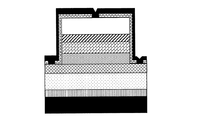
- FIG. 1 is a cross-sectional view of a solar cell element 9 according to an embodiment.
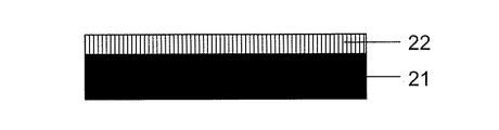
- FIG. 2 is a cross-sectional view of one step included in the method for manufacturing the solar cell element 9.
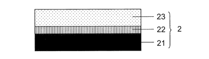
- FIG. 3 is a cross-sectional view of one step included in the method of manufacturing the solar cell element 9 following FIG.
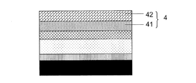
- FIG. 4 is a cross-sectional view of one step included in the method for manufacturing the solar cell element 9 following FIG.
- FIG. 5 is a cross-sectional view of one step included in the method for manufacturing the solar cell element 9 subsequent to FIG. 4.
- FIG. 6 is a cross-sectional view of one step included in the method for manufacturing the solar cell element 9 following FIG.
- FIG. 7 is a cross-sectional view of one step included in the method for manufacturing the solar cell element 9 subsequent to FIG. 6.
- FIG. 8 is a cross-sectional view of one step included in the method of manufacturing the solar cell element 9 following FIG.
- FIG. 9 is a cross-sectional view of one step included in the method for manufacturing the solar cell element 9 following FIG.
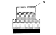
- FIG. 10 is a cross-sectional view of one step included in the method for manufacturing the solar cell element 9 subsequent to FIG. 9.
- FIG. 11 is a cross-sectional view of one step included in the method for manufacturing the solar cell element 9 following FIG.
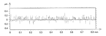
- FIG. 12 is a diagram illustrating an example of a surface roughness profile.
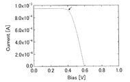
- FIG. 13 shows the IV curve obtained in Example 1.
- FIG. 14 is a cross-sectional view of a solar cell element disclosed in Patent Document 1.
- FIG. 15 is a diagram for explaining Ra.
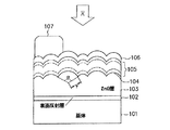
- FIG. 16 is an enlarged cross-sectional view of a portion surrounded by a broken line A drawn in FIG.
- FIG. 17 is a diagram showing an SEM image of the Li x Ag 1-x layer 22 according to the first example.
- a method of generating electric power using the solar cell element according to the first aspect of the present disclosure includes a transparent substrate body, a Li x Ag 1-x layer, a ZnO layer, a transparent conductive layer, and a photoelectric conversion layer.
- a step of preparing solar cell elements stacked in order The photoelectric conversion layer includes an n-type semiconductor layer and a p-type semiconductor layer, The solar cell element further includes an n-side electrode electrically connected to the n-type semiconductor layer, and a p-side electrode electrically connected to the p-type semiconductor layer,
- x represents a value of 0.001 or more and 0.05 or less
- the Li x Ag 1-x layer has a thickness of 2 nanometers or more and 15 nanometers or less
- the ZnO layer has an arithmetic average roughness of 20 nanometers or more and 760 nanometers or less
- the ZnO layer is composed of a plurality of ZnO columnar crystal grains grown on the surface of the Li x
- the photoelectric conversion layer is irradiated with light through the transparent substrate body, the Li x Ag 1-x layer, the ZnO layer, and the transparent conductive layer, and between the n-side electrode and the p-side electrode.
- a step (b) of generating electric power including.
- the method for generating electric power using the solar cell element according to the second aspect of the present disclosure further includes a back electrode layer in the first aspect, and the photoelectric conversion layer includes the back electrode layer and the transparent conductive layer. It may be sandwiched between layers.
- the method for generating electric power using the solar cell element according to the third aspect of the present disclosure is the second aspect, wherein the n-type semiconductor layer is sandwiched between the transparent conductive layer and the p-type semiconductor layer, The p-type semiconductor layer may be sandwiched between the n-type semiconductor layer and the back electrode layer.
- the method for generating electric power using the solar cell element according to the fourth aspect of the present disclosure is that, in the third aspect, the n-side electrode is formed on the transparent conductive layer, and the p-side electrode is , And may be formed on the back electrode layer.
- the method of generating electric power using the solar cell element according to the fifth aspect of the present disclosure is the first aspect, wherein the ZnO layer has a volume resistivity of 1 ⁇ 10 ⁇ 3 ⁇ ⁇ cm or more. Good.
- the method for generating electric power using the solar cell element according to the sixth aspect of the present disclosure is the first aspect, wherein the transparent conductive layer has a volume resistivity of less than 1 ⁇ 10 ⁇ 3 ⁇ ⁇ cm. Also good.
- the ZnO layer has a volume resistivity of 1 ⁇ 10 ⁇ 3 ⁇ ⁇ cm or more
- the transparent conductive layer may be made of ZnO having a volume resistivity of less than 1 ⁇ 10 ⁇ 3 ⁇ ⁇ cm.
- the light may be sunlight in the first aspect.
- a solar cell element according to a ninth aspect of the present disclosure is a solar cell element in which a transparent substrate body, a Li x Ag 1-x layer, a ZnO layer, a transparent conductive layer, and a photoelectric conversion layer are sequentially stacked.
- the photoelectric conversion layer includes an n-type semiconductor layer and a p-type semiconductor layer
- the solar cell element further includes an n-side electrode electrically connected to the n-type semiconductor layer, and a p-side electrode electrically connected to the p-type semiconductor layer
- x represents a value of 0.001 or more and 0.05 or less
- the Li x Ag 1-x layer has a thickness of 2 nanometers or more and 15 nanometers or less
- the ZnO layer has an arithmetic average roughness of 20 nanometers or more and 760 nanometers or less
- the ZnO layer is composed of a plurality of ZnO columnar crystal grains grown on the surface of the Li x Ag 1-x layer, Each ZnO columnar crystal grain has a longitudinal direction along the normal direction of the transparent substrate body, Each of the ZnO columnar crystal grains has a width that increases from the Li x Ag 1-x layer toward the transparent conductive layer, The width of each ZnO columnar crystal grain appears
- the solar cell element according to a tenth aspect of the present disclosure in the ninth aspect, further includes a back electrode layer, and the photoelectric conversion layer is sandwiched between the back electrode layer and the transparent conductive layer. Also good.
- the n-type semiconductor layer is sandwiched between the transparent conductive layer and the p-type semiconductor layer, and the p-type semiconductor layer is It may be sandwiched between the n-type semiconductor layer and the back electrode layer.
- the n-side electrode is formed on the transparent conductive layer
- the p-side electrode is formed on the back electrode layer. May be.
- the ZnO layer may have a volume resistivity of 1 ⁇ 10 ⁇ 3 ⁇ ⁇ cm or more.
- the transparent conductive layer may have a volume resistivity of less than 1 ⁇ 10 ⁇ 3 ⁇ ⁇ cm.
- the ZnO layer has a volume resistivity of 1 ⁇ 10 ⁇ 3 ⁇ ⁇ cm or more
- the transparent conductive layer may be made of ZnO having a volume resistivity of less than 1 ⁇ 10 ⁇ 3 ⁇ ⁇ cm.
- FIG. 1 is a cross-sectional view of a solar cell element 9 according to an embodiment.
- the solar cell element 9 includes a transparent substrate 2, a transparent conductive layer 3, a photoelectric conversion layer 4, a back electrode layer 5, an n-side electrode 6, and a p-side electrode 7 in this order.
- the transparent substrate 2 includes a transparent substrate body 21, a Li x Ag 1-x layer 22, and a ZnO layer 23.
- the Li x Ag 1-x layer 22 is sandwiched between the transparent substrate body 21 and the ZnO layer 23.
- the transparent substrate body 21 is desirably transmissive to light (for example, sunlight) having a wavelength of 300 nanometers or more and 1100 nanometers or less.
- Examples of the transparent substrate body 21 are a glass substrate, a ceramic substrate, a plastic substrate, or a metal substrate.
- the transparent substrate body 21 is preferably a glass substrate having a thickness of 0.3 to 7 millimeters from the viewpoint of strength and heat resistance.
- Li x Ag 1-x layer 22 The Li x Ag 1-x layer 22 is made of an alloy of lithium and silver.
- the letter “x” represents a value between 0.001 and 0.05. When the value of x is less than 0.001, the photoelectric conversion efficiency decreases (for example, see Comparative Example 3). Similarly, when the value of x exceeds 0.05, the photoelectric conversion efficiency decreases (see, for example, Comparative Example 4).
- the Li x Ag 1-x layer 22 has a thickness of 2 nanometers or more and 15 nanometers or less. Since the Li x Ag 1-x layer 22 is very thin, the Li x Ag 1-x layer 22 is transparent to light. When the Li x Ag 1-x layer 22 is not provided, the photoelectric conversion efficiency decreases. When the Li x Ag 1-x layer 22 has a thickness exceeding 15 nanometers, the photoelectric conversion efficiency decreases.
- the Li x Ag 1-x layer 22 may be formed by sputtering.
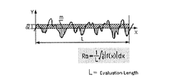
- the ZnO layer 23 has an arithmetic average roughness (hereinafter referred to as “Ra”) of 20 nanometers or more and 760 nanometers or less.
- Arithmetic mean roughness Ra is the arithmetic mean of the absolute value of the distance from the mean line to the surface roughness profile.
- Ra is represented by the following formula (I):
- L is the evaluation length
- f (x) is the surface roughness profile. Note that x represents coordinates in a one-dimensional direction parallel to the surface.
- FIG. 15 is a diagram for explaining the arithmetic average roughness Ra.
- the value of Ra may be measured using a surface roughness measuring instrument.
- the surface roughness measuring instrument is available from Taylor Hobson as the trade name “CCI Lite”.
- the surface roughness profile f (x) is a profile obtained by measuring the uneven shape of the surface of the object using a surface roughness measuring instrument.
- FIG. 12 is a diagram illustrating an example of a surface roughness profile.
- ZnO is transparent. Therefore, the ZnO layer 23 is transparent to light.
- the ZnO layer 23 is composed of a plurality of ZnO columnar crystal grains 23a.
- Each ZnO columnar crystal grain 23a is grown using Ag contained in the Li x Ag 1-x layer 22 as a nucleus. Li contained in the Li x Ag 1-x layer 22 improves the crystallinity of the ZnO columnar crystal grains 23a.
- Each ZnO columnar crystal grain 23 a has a longitudinal direction along the normal direction of the transparent substrate body 21.
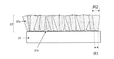
- Each ZnO columnar crystal grain 23 a has a width that increases from the Li x Ag 1-x layer 22 toward the transparent conductive layer 3. Specifically, each ZnO columnar crystal grain 23a has an R2 / R1 ratio of 1.1 or more and 1.6 or less. As shown in FIG. 16, the value of R1 represents the width of one end of the ZnO columnar crystal grain 23a in contact with the surface of the Li x Ag 1-x layer 22. The value of R2 represents the width of the other end of the ZnO columnar crystal grains in contact with the ZnO layer 3. When the R2 / R1 ratio is less than 1.1, the photoelectric conversion efficiency decreases (for example, see Comparative Example 1). When R2 / R1 exceeds 1.6, the photoelectric conversion efficiency decreases (for example, see Comparative Example 2).
- the width of the ZnO columnar crystal grain 23 a appears by cutting the ZnO columnar crystal grain 23 a along the normal direction of the transparent substrate body 21. This width is substantially orthogonal to the longitudinal direction of the ZnO columnar crystal grains 23a.
- the ZnO layer 23 has a volume resistivity of 1 ⁇ 10 ⁇ 3 ⁇ ⁇ cm or more.
- Transparent conductive layer 3 The transparent conductive layer 3 is sandwiched between the ZnO layer 23 and the photoelectric conversion layer 4.
- An example of the material of the transparent conductive layer 3 is zinc oxide doped with at least one selected from the group consisting of gallium, aluminum, and boron.
- the transparent conductive layer 3 has a volume resistivity of less than 1 ⁇ 10 ⁇ 3 ⁇ ⁇ cm. Since the ZnO layer 23 has a large volume resistivity, it is difficult to efficiently obtain electricity from the ZnO layer 23. Therefore, it is desirable to provide such a low resistance transparent conductive layer 3.
- the photoelectric conversion layer 4 includes an n-type semiconductor layer 41 and a p-type semiconductor layer 42.
- An example of the material of the n-type semiconductor layer 41 is silicon or GaAs.
- An example of the material of the p-type semiconductor layer 42 is also silicon or GaAs.
- an n-type semiconductor layer 41 and a p-type semiconductor layer 42 are formed in this order on the transparent conductive layer 3.
- the n-type semiconductor layer 41 is in contact with the p-type semiconductor layer 42 and forms a pn junction.
- the solar cell element 9 may include a back electrode layer 5.
- the back electrode layer 5 may include a buffer layer 51 and a reflective layer 52.
- the buffer layer 51 is sandwiched between the photoelectric conversion layer 42 and the reflective layer 52.
- the material of the buffer layer 51 include (a) a transparent conductive material such as zinc oxide, indium oxide, tin oxide, or cadmium oxide, or (b) iron oxide, titanium oxide, zinc selenide, or zinc sulfide. Such a transparent semiconductor material.
- the buffer layer 51 is preferably zinc oxide.
- Examples of the material of the reflective layer 52 are gold, silver, copper, aluminum, platinum, or an alloy thereof. As the reflective layer 52, silver is desirable.
- N-side electrode 6 The n-side electrode 6 is electrically connected to the n-type semiconductor layer 41. In FIG. 1, the n-side electrode 6 forms an ohmic connection with the transparent conductive layer 3. Examples of suitable materials for the n-side electrode 6 are silver, gold, copper, aluminum, platinum, or alloys thereof. As the n-side electrode 6, platinum is desirable.
- the p-side electrode 7 is electrically connected to the p-type semiconductor layer 42. In FIG. 1, the p-side electrode 7 forms an ohmic connection with the reflective layer 52. Examples of suitable materials for the p-side electrode 7 are silver, gold, copper, aluminum, platinum, or alloys thereof. As the p-side electrode 7, platinum is desirable.
- a transparent substrate body 21 is prepared.
- a glass substrate is desirable.
- a Li x Ag 1-x layer 22 is formed on the surface of the transparent substrate main body 21 by a general semiconductor growth method such as an RF magnetron sputtering method or a vacuum evaporation method.
- the Li x Ag 1-x layer 22 is heated.
- the heating method are an annealing method, a vacuum heating method, a UV ozone method, an accelerated oxidation treatment method, an annealing method in an oxygen atmosphere, or an anodic oxidation method.
- an annealing method at a temperature of 50 to 800 ° C. is desirable.
- the width of the Li x Ag 1-x layer 23 is reduced. In other words, the area of the Li x Ag 1-x layer 22 is reduced by the heat treatment. In this manner, island-shaped Li x Ag 1-x regions 22 are formed on the transparent substrate body 21.
- the Li x Ag 1-x layer 22 may not cover the entire surface of the transparent substrate body 21.
- the uncoated portion 21b of the transparent substrate body 21 may be exposed.
- FIG. 16 is an enlarged view of a portion surrounded by a broken line A drawn in FIG.
- the ZnO layer 23 is composed of a plurality of ZnO columnar crystal grains 23a. Since each ZnO columnar crystal grain 23a has an R2 / R1 ratio of 1.1 or more and 1.6 or less, the upper surface of the ZnO layer 23 has no gap.
- the Li x Ag 1-x layer 22 and the portion 21 b of the transparent substrate body 21 that is not covered with the ZnO layer 23 may be exposed.
- the surface roughness of the Li x Ag 1-x layer 22 may be changed depending on the temperature of the heat treatment.
- the ZnO layer 23 is obtained by a CBD method using a mixed solution of Zn (NO 3 ) 2 and hexamethylenetetramine (hereinafter referred to as “HMT”) at a temperature of 20 to 90 ° C. , Formed on the Li x Ag 1-x layer 22.
- HMT hexamethylenetetramine
- the surface roughness of the formed ZnO layer 23 increases.
- reactive ion etching CH 4 gas may be used.
- chemical etching a chloride solution may be used.
- the ZnO layer 23 is in contact with the Li x Ag 1-x layer 22. More precisely, the ZnO layer 23 is in contact with the upper surface of the Li x Ag 1-x layer 22.
- the transparent conductive layer 3 is uniformly formed on the ZnO layer 23.
- An example of a method for forming the transparent conductive layer 3 is a pulse laser deposition method (hereinafter referred to as “PLD method”).
- an n-type silicon layer 41 and a p-type silicon layer 42 are deposited on the transparent conductive layer 3 in this order by the plasma CVD method to form the photoelectric conversion layer 4.
- the n-type silicon layer 41 may be formed by a plasma CVD method using a mixed gas containing phosphine, silane, and hydrogen.
- the p-type silicon layer 41 is deposited by a plasma CVD method using a mixed gas containing diborane, silane, methane, and hydrogen.
- the back electrode layer 5 including the buffer layer 51 and the reflective layer 52 is formed.
- An example of a method for forming the buffer layer 51 is a PLD method, an RF magnetron sputtering method, or a vacuum evaporation method.
- An example of a method for forming the reflective layer 52 is an RF magnetron sputtering method or a vacuum deposition method.
- a first mask 81 is formed on the upper surface of the stacked body 1 by photolithography.
- the unnecessary part of the laminated body 1 is removed by an etching. More specifically, unnecessary portions of the reflective layer 52 and unnecessary portions of the buffer layer 51 are removed by wet etching using a mixed solution of hydrochloric acid and nitric acid. Furthermore, using this resist film as the first mask 81, unnecessary portions of the photoelectric conversion layer 4 are removed by ICP plasma etching using a mixed gas of oxygen, argon, and SF 6 .
- the second mask 82 is formed by photolithography.
- the second mask 82 has a first opening 821 and a second opening 822.
- the transparent conductive layer 3 is located below the first opening 821.
- the reflective layer 52 is located below the second opening 822.
- a metal layer is formed on the second mask 82 by a sputter deposition method or an electron beam deposition method. Finally, as shown in FIG. 11, the second mask 82 is removed. In this way, the n-side electrode 6 and the p-side electrode 7 are formed.
- the transparent substrate body 21 is irradiated with light.
- the light passes through the transparent substrate main body 21, the Li x Ag 1-x layer 22, the ZnO layer 23, and the transparent conductive layer 3 and reaches the photoelectric conversion layer 4.
- Light is converted into electricity by the photoelectric conversion layer 4. In this way, electric power is generated between the n-side electrode 6 and the p-side electrode 7.
- Example 1 the solar cell element 9 shown in FIG. 1 was produced by the method shown in FIGS. 2 to 11 as follows.
- a glass substrate having a thickness of 5 mm was prepared as the transparent substrate body 21.
- the transparent substrate body 21 had a length of 25 millimeters and a width of 25 millimeters.
- the transparent substrate body 21 had a light transmittance of 88 to 90%.
- the transparent substrate body 21 was immersed in ethanol and washed under application of ultrasonic waves.
- RF magnetron sputtering method a mixed target of Li and Ag having a molar ratio of 1: 999 was used.
- the formed Li x Ag 1-x layer 22 had a thickness of 2 nanometers.
- the transparent substrate main body 21 thus obtained was heated at a temperature of 350 ° C. for 10 minutes.
- the transparent substrate body 21 is immersed in a mixed solution of Zn (NO 3 ) 2 and HMT heated to 70 ° C. for 3 hours, and a ZnO layer 23 is formed on the transparent substrate body 21.
- Zn (NO 3 ) 2 had a concentration of 0.1M.
- HMT also had a concentration of 0.1M.
- the formed ZnO layer 23 had a thickness of 1 micrometer.
- Ra of the formed ZnO layer 23 was measured using a surface roughness measuring instrument (available from Taylor Hobson, trade name “CCI Lite”). As a result, the value of Ra was 21 nanometers.
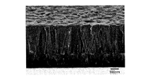
- FIG. 17 is a diagram showing an SEM image of the ZnO layer 23 included in the cut laminate 1. Based on FIG. 17, the values of R1 and R2 were measured.
- the value of R1 was 117 nanometers.
- the value of R2 was 152 nanometers. Therefore, the R2 / R1 ratio was approximately 1.3.
- volume resistivity RE ⁇ t ⁇ RCF
- RE represents a resistance value measured by a four-terminal measurement method.
- a measuring instrument for measuring the resistance value based on the four-terminal measurement method is available from Mitsubishi Chemical Corporation under the trade name: Loresta-Gp MCP-T610.
- the value of t represents the thickness of the ZnO layer 23.
- RCF represents a correction coefficient (Resistivity Correction Factor). In this example, the RCF value was 4.398.
- the ZnO layer 23 had a volume resistivity of 9.92 ⁇ 10 ⁇ 3 ⁇ ⁇ cm.
- the transparent conductive layer 3 was formed on the ZnO layer 23 by the PLD method.
- the material of the transparent conductive layer 3 is zinc oxide doped with 5.7% by mass of gallium.
- zinc oxide doped with gallium is referred to as “GZO”.
- the transparent conductive layer 3 had a thickness of 100 nanometers.
- the volume resistivity of the transparent conductive layer 3 was measured in the same manner as the ZnO layer 23. As a result, the transparent conductive layer 3 had a volume resistivity of 5.2 ⁇ 10 ⁇ 4 ⁇ ⁇ cm.
- an n-type semiconductor layer 41 made of n-type silicon and a p-type semiconductor layer 42 made of p-type silicon were formed in this order by the plasma CVD method to form the photoelectric conversion layer 4.
- the n-type semiconductor layer 41 had a thickness of 40 nanometers.
- the p-type semiconductor layer 42 had a thickness of 11 nanometers.
- a GZO film having a thickness of 40 nanometers was formed on the p-type semiconductor layer 42 by a sputter deposition method. In this way, a buffer layer 51 made of a GZO film was formed.
- a silver layer having a thickness of 200 nanometers was formed on the buffer layer 51 by a sputter deposition method. In this way, a reflective layer 52 made of silver was formed.
- a 20 mm square resist film 81 was formed on the reflective layer 52 by photolithography.
- this resist film as the first mask 81, unnecessary portions of the reflective layer 52 and unnecessary portions of the buffer layer 51 were removed by wet etching using a mixed solution of hydrochloric acid and nitric acid.
- the first mask 81 was removed.
- the second mask 82 was formed by photolithography.
- the second mask 82 had a first opening 821 and a second opening 822.
- the first opening 821 was provided on the transparent conductive layer 3.
- the first opening 821 had a size of 22 millimeters square.
- a second opening 822 was provided on the reflective layer 52.
- the second opening 822 had a size of 2 millimeters ⁇ 20 millimeters.
- a platinum film having a thickness of 100 nanometers was formed, and the second mask 82 was covered with the platinum film.
- the second mask 82 was removed, and an n-side electrode 6 made of platinum and a p-side electrode 7 made of platinum were formed.
- the solar cell element 9 was obtained.
- the transparent substrate body 21 was irradiated with pseudo-sunlight described later.
- the photoelectric conversion efficiency of the solar cell element 9 was calculated as follows.
- the pseudo-sunlight having an output energy of 100 mW / cm 2 was irradiated to the transparent substrate body 21.
- the simulated sunlight was emitted from a lamp combining a 500 watt xenon lamp (available from Wacom Denso Co., Ltd.) and a 400 watt halogen lamp (available from Wacom Denso Co., Ltd.).
- the open circuit voltage Voc open circuit voltage when the space between the n-side electrode 6 and the p-side electrode 7 was opened was measured.
- a short-circuit current I SC (short-circuit current) when the n-side electrode 6 and the p-side electrode 7 were short-circuited was measured.
- FF fill factor
- the curve factor FF is calculated from the following equation.
- V max means a voltage when the value of V ⁇ I of the IV curve is maximum in FIG. 13 (see the arrow in FIG. 13).
- I max means a current when the value of V ⁇ I of the IV curve is maximized (see the arrow in FIG. 13).
- Example 2 An experiment similar to that of Example 1 was performed, except that the Li 0.001 Zn 0.999 layer had a thickness of 15.4 nanometers. The results are shown in Table 1.
- Example 3 An experiment similar to that in Example 1 was performed, except that the ZnO layer 23 was formed using a mixed solution of 0.05M Zn (NO 3 ) 2 and 0.05M HMT. The results are shown in Table 1.
- Example 4 An experiment similar to that in Example 1 was performed, except that the ZnO layer 23 was formed using a mixed solution of 0.75M Zn (NO 3 ) 2 and 0.75M HMT. The results are shown in Table 1.
- Example 1 An experiment similar to that in Example 1 was performed, except that the ZnO layer 23 was formed using a mixed solution of 0.01M Zn (NO 3 ) 2 and 0.01M HMT. The results are shown in Table 2.
- Example 2 An experiment similar to that of Example 1 was performed except that the ZnO layer 23 was formed using a mixed solution of 1M Zn (NO 3 ) 2 and 1M HMT. The results are shown in Table 2.
- Example 5 An experiment similar to that in Example 1 was performed, except that the Li x Ag 1-x layer 22 was not provided. The results are shown in Table 2.
- Example 7 Example 1 except that instead of the Li x Ag 1-x layer 22, ZnO nanoparticles having an average particle diameter (d50) of 2.2 nanometers were applied on the transparent substrate body 21 by the spin coater method. A similar experiment was conducted. The formed film had a thickness of 2.2 nanometers. ZnO nanoparticles were synthesized by a sol-gel method. The results are shown in Table 3.
- Table 1 shows the results of Examples 1 to 5.
- Table 2 shows the results of Comparative Examples 1 to 5.
- Table 3 shows the results of Comparative Examples 6 and 7.
- the solar cell element has high photoelectric conversion efficiency when all of the following conditions (A) to (D) are satisfied.
- the present disclosure provides a solar cell element having high photoelectric conversion efficiency.
- Laminated body 2 Transparent substrate 21: Transparent substrate body 22: Li x Ag 1-x layer 23: ZnO layer 3: Transparent conductive layer 4: Photoelectric conversion layer 41: n-type semiconductor layer 42: p-type semiconductor layer 5: Back electrode layer 51: Buffer layer 52: Reflective layer 6: n-side electrode 7: p-side electrode 81: first mask 82: second mask 821: first opening 822; second opening 9: solar cell element
Landscapes
- Photovoltaic Devices (AREA)
- Life Sciences & Earth Sciences (AREA)
- Engineering & Computer Science (AREA)
- Sustainable Development (AREA)
- Sustainable Energy (AREA)
Abstract
L'invention concerne un élément de cellule solaire, obtenu par stratification, dans l'ordre, d'un corps de substrat transparent, d'une couche LixAg1-x (où 0,001 ≤ x ≤ 0,05), d'une couche ZnO, d'une couche conductrice transparente et d'une couche de conversion photoélectrique, la couche de conversion photoélectrique comprenant une couche à semi-conducteurs de type n et une couche à semi-conducteurs de type p et elle est dotée d'une électrode de côté n, électriquement connectée à la couche à semi-conducteurs de type n, et d'une électrode de côté p, électriquement connectée au semi-conducteur de type p. La couche LixAg1-x présente une épaisseur comprise entre 2 nm et 15 nm. La couche ZnO présente une rugosité arithmétique moyenne comprise entre 20 nm et 70 nm. La couche ZnO est composée de multiples grains basaltiques ZnO ayant grandi sur la surface de la couche LixAg1-x. Chaque grain basaltique ZnO a une direction longitudinale le long de la direction normale du corps de substrat transparent et une largeur qui augmente vers la couche conductrice transparente depuis la couche LixAg1-x. La largeur de chaque grain basaltique ZnO émerge en résultat de la découpe de chaque grain basaltique ZnO le long de la direction normale du corps de substrat transparent. Chaque grain basaltique ZnO a un rapport R2/R1 compris entre 1,1 et 1,6, où R1 représente la largeur d'une extrémité du grain basaltique ZnO qui touche la surface de la couche LixAg1-x et R2 représente la largeur de l'autre extrémité du grain basaltique ZnO.
Priority Applications (2)
| Application Number | Priority Date | Filing Date | Title |
|---|---|---|---|
| JP2013533428A JP5390731B1 (ja) | 2012-04-17 | 2013-03-26 | 太陽電池素子、及び、太陽電池素子を用いて電力を発生させる方法 |
| US14/143,294 US9024178B2 (en) | 2012-04-17 | 2013-12-30 | Solar cell element |
Applications Claiming Priority (2)
| Application Number | Priority Date | Filing Date | Title |
|---|---|---|---|
| JP2012093610 | 2012-04-17 | ||
| JP2012-093610 | 2012-04-17 |
Related Child Applications (1)
| Application Number | Title | Priority Date | Filing Date |
|---|---|---|---|
| US14/143,294 Continuation US9024178B2 (en) | 2012-04-17 | 2013-12-30 | Solar cell element |
Publications (1)
| Publication Number | Publication Date |
|---|---|
| WO2013157204A1 true WO2013157204A1 (fr) | 2013-10-24 |
Family
ID=49383179
Family Applications (1)
| Application Number | Title | Priority Date | Filing Date |
|---|---|---|---|
| PCT/JP2013/002055 Ceased WO2013157204A1 (fr) | 2012-04-17 | 2013-03-26 | Elément de cellule solaire et procédé de génération d'énergie à l'aide de celui-ci |
Country Status (3)
| Country | Link |
|---|---|
| US (1) | US9024178B2 (fr) |
| JP (1) | JP5390731B1 (fr) |
| WO (1) | WO2013157204A1 (fr) |
Families Citing this family (1)
| Publication number | Priority date | Publication date | Assignee | Title |
|---|---|---|---|---|
| WO2013150708A1 (fr) * | 2012-04-02 | 2013-10-10 | パナソニック株式会社 | Élément de cellule solaire et son procédé de fabrication |
Citations (3)
| Publication number | Priority date | Publication date | Assignee | Title |
|---|---|---|---|---|
| JPH11220154A (ja) * | 1997-10-29 | 1999-08-10 | Canon Inc | 光起電力素子および光起電力素子モジュール |
| JP2002280084A (ja) * | 2001-03-15 | 2002-09-27 | Canon Inc | 光電変換装置およびその製造方法 |
| JP2004311704A (ja) * | 2003-04-07 | 2004-11-04 | Kanegafuchi Chem Ind Co Ltd | 薄膜光電変換装置用基板及びそれを用いた薄膜光電変換装置 |
Family Cites Families (2)
| Publication number | Priority date | Publication date | Assignee | Title |
|---|---|---|---|---|
| US5731661A (en) * | 1996-07-15 | 1998-03-24 | Motorola, Inc. | Passivation of electroluminescent organic devices |
| EP0915523A3 (fr) | 1997-10-29 | 2005-11-02 | Canon Kabushiki Kaisha | Elément photovoltaique comportant une couche arrière transparente et conductrice de courant avec une région superficielle ayant une section transversale déterminée et un module comprenant cet élément photovoltaique |
-
2013
- 2013-03-26 WO PCT/JP2013/002055 patent/WO2013157204A1/fr not_active Ceased
- 2013-03-26 JP JP2013533428A patent/JP5390731B1/ja not_active Expired - Fee Related
- 2013-12-30 US US14/143,294 patent/US9024178B2/en not_active Expired - Fee Related
Patent Citations (3)
| Publication number | Priority date | Publication date | Assignee | Title |
|---|---|---|---|---|
| JPH11220154A (ja) * | 1997-10-29 | 1999-08-10 | Canon Inc | 光起電力素子および光起電力素子モジュール |
| JP2002280084A (ja) * | 2001-03-15 | 2002-09-27 | Canon Inc | 光電変換装置およびその製造方法 |
| JP2004311704A (ja) * | 2003-04-07 | 2004-11-04 | Kanegafuchi Chem Ind Co Ltd | 薄膜光電変換装置用基板及びそれを用いた薄膜光電変換装置 |
Also Published As
| Publication number | Publication date |
|---|---|
| US20140109964A1 (en) | 2014-04-24 |
| JPWO2013157204A1 (ja) | 2015-12-21 |
| US9024178B2 (en) | 2015-05-05 |
| JP5390731B1 (ja) | 2014-01-15 |
Similar Documents
| Publication | Publication Date | Title |
|---|---|---|
| CN107710419A (zh) | 太阳能电池和太阳能电池模块 | |
| CN101572279A (zh) | 溅射法生长高迁移率绒面结构IMO/ZnO复合薄膜及太阳电池应用 | |
| Knight et al. | Soft imprinted Ag nanowire hybrid electrodes on silicon heterojunction solar cells | |
| Alkallas et al. | Enhancing photovoltaic cell efficiency: a comprehensive study on BN-Si3N4 blend antireflective coatings and their impact on power conversion | |
| Hsueh et al. | Crystalline-Si photovoltaic devices with ZnO nanowires | |
| CN102496639B (zh) | 等离激元增强型中间带太阳能电池及其光电转换薄膜材料 | |
| Chen et al. | Optimizing transparent conductive Al-doped ZnO thin films for SiNx free crystalline Si solar cells | |
| JP5390731B1 (ja) | 太陽電池素子、及び、太陽電池素子を用いて電力を発生させる方法 | |
| JP5426056B1 (ja) | 太陽電池素子、及び、太陽電池素子を用いて電力を発生させる方法 | |
| JP5408397B1 (ja) | 太陽電池素子およびその製造方法 | |
| JP2013254845A (ja) | 太陽電池素子 | |
| US20150325712A1 (en) | Nanostructured Thin-Film Solar Cell | |
| Baral et al. | Stacked back reflector architecture for advanced optical management in State-of-the-art single-junction μc-Si: H solar cells | |
| JP2013258293A (ja) | 太陽電池素子 | |
| JP2014003111A (ja) | 太陽電池素子 | |
| JP2013222867A (ja) | 太陽電池素子 | |
| JP5405923B2 (ja) | 光電変換素子及びその製造方法 | |
| Galib Hashmi et al. | Fabrication of crystalline silicon solar cell in Bangladesh: limitations and remedies | |
| TWI467782B (zh) | 薄膜太陽能電池 | |
| JP5818789B2 (ja) | 薄膜太陽電池 | |
| Oswal et al. | Study of Performance Analysis of Modern Materials for Transparent Thin Film Solar Cells | |
| CN107302038A (zh) | 一种实现表面等离子激元增强型纳米结构薄膜太阳电池的方法 | |
| JP5307280B2 (ja) | 薄膜光電変換素子 | |
| KR101482391B1 (ko) | 박막형 태양전지용 기판의 제조방법 | |
| TWI387117B (zh) | 太陽能電池裝置及其製造方法 |
Legal Events
| Date | Code | Title | Description |
|---|---|---|---|
| ENP | Entry into the national phase |
Ref document number: 2013533428 Country of ref document: JP Kind code of ref document: A |
|
| 121 | Ep: the epo has been informed by wipo that ep was designated in this application |
Ref document number: 13777884 Country of ref document: EP Kind code of ref document: A1 |
|
| NENP | Non-entry into the national phase |
Ref country code: DE |
|
| 122 | Ep: pct application non-entry in european phase |
Ref document number: 13777884 Country of ref document: EP Kind code of ref document: A1 |