WO2013161069A1 - Module de photopile et procédé de production d'un module de photopile - Google Patents
Module de photopile et procédé de production d'un module de photopile Download PDFInfo
- Publication number
- WO2013161069A1 WO2013161069A1 PCT/JP2012/061421 JP2012061421W WO2013161069A1 WO 2013161069 A1 WO2013161069 A1 WO 2013161069A1 JP 2012061421 W JP2012061421 W JP 2012061421W WO 2013161069 A1 WO2013161069 A1 WO 2013161069A1
- Authority
- WO
- WIPO (PCT)
- Prior art keywords
- cell module
- tab
- solar cell
- region
- solar
- Prior art date
- Legal status (The legal status is an assumption and is not a legal conclusion. Google has not performed a legal analysis and makes no representation as to the accuracy of the status listed.)
- Ceased
Links
Images




Classifications
-
- H—ELECTRICITY
- H10—SEMICONDUCTOR DEVICES; ELECTRIC SOLID-STATE DEVICES NOT OTHERWISE PROVIDED FOR
- H10F—INORGANIC SEMICONDUCTOR DEVICES SENSITIVE TO INFRARED RADIATION, LIGHT, ELECTROMAGNETIC RADIATION OF SHORTER WAVELENGTH OR CORPUSCULAR RADIATION
- H10F19/00—Integrated devices, or assemblies of multiple devices, comprising at least one photovoltaic cell covered by group H10F10/00, e.g. photovoltaic modules
- H10F19/90—Structures for connecting between photovoltaic cells, e.g. interconnections or insulating spacers
- H10F19/902—Structures for connecting between photovoltaic cells, e.g. interconnections or insulating spacers for series or parallel connection of photovoltaic cells
-
- Y—GENERAL TAGGING OF NEW TECHNOLOGICAL DEVELOPMENTS; GENERAL TAGGING OF CROSS-SECTIONAL TECHNOLOGIES SPANNING OVER SEVERAL SECTIONS OF THE IPC; TECHNICAL SUBJECTS COVERED BY FORMER USPC CROSS-REFERENCE ART COLLECTIONS [XRACs] AND DIGESTS
- Y02—TECHNOLOGIES OR APPLICATIONS FOR MITIGATION OR ADAPTATION AGAINST CLIMATE CHANGE
- Y02E—REDUCTION OF GREENHOUSE GAS [GHG] EMISSIONS, RELATED TO ENERGY GENERATION, TRANSMISSION OR DISTRIBUTION
- Y02E10/00—Energy generation through renewable energy sources
- Y02E10/50—Photovoltaic [PV] energy
Definitions
- the present invention relates to a solar cell module and a method for manufacturing the solar cell module.
- solar cells examples include single crystal solar cells, polycrystalline solar cells, amorphous solar cells, and the like, or combinations thereof. Usually, a plurality of solar cells are connected in series or in parallel and used as a solar cell module.
- the solar cell module 100 has a structure in which a plurality of solar cells 10 are connected by tabs 12.
- the tab 12 connects the first electrode 14 on the light receiving surface side of the solar battery cell 10 and the second electrode 16 on the back surface side of the adjacent solar battery cell 10.
- the tab 12 has a bent portion 12 a in order to provide a step corresponding to the thickness of the solar battery cell 10.
- One aspect of the present invention is a solar cell module including a plurality of solar cells and a tab connecting the plurality of solar cells, and the tab is another region in the peripheral portion of the solar cell.
- the region has a smaller crystal grain size.
- Another aspect of the present invention is a method for manufacturing a solar cell module, wherein the first step of making the crystal grain size of a partial region of the tab smaller than the other region, and the region where the crystal grain size is made small are solar. And a second step of connecting the plurality of solar battery cells with tabs so as to be arranged at the peripheral edge of the battery cell.
- the tab in a solar cell module including solar cells connected by a tab, the tab can be prevented from being damaged, and the reliability of the solar cell module can be improved.
- the solar cell module 200 in the embodiment of the present invention includes a solar cell 20, a tab 22, an adhesive 24, a first protection member 26, and a second protection.
- the member 28 and the filler 30 are included.
- FIG. 1 is a plan view of the solar cell module 200 viewed from the light receiving surface side
- FIG. 2 is a schematic cross-sectional view taken along line AA in FIG.
- the “light receiving surface” is one of the main surfaces of the solar battery cell 20 and means a surface on which light from the outside is mainly incident. For example, 50% to 100% of the light incident on the solar battery cell 20 enters from the light receiving surface side.
- the “back surface” is one of the main surfaces of the solar battery cell 20 and means a surface opposite to the light receiving surface.
- the solar battery cell 20 receives light such as sunlight to generate carriers (electrons and holes), a first electrode 20b provided on the light receiving surface of the photoelectric conversion unit 20a, And a second electrode 20c provided on the back surface of the photoelectric conversion unit 20a.
- the first electrode 20 b and the second electrode 20 c include fingers provided in a comb shape so as to intersect the extending direction of the tab 22 and bus bars connecting the fingers.
- the bus bar is provided to cover the tab 22.
- the fingers and bus bars are formed, for example, by screen-printing a conductive paste in which a conductive filler such as silver (Ag) is dispersed in a binder resin in a desired pattern on a transparent conductive layer.
- a metal film such as a silver (Ag) thin film may be formed on substantially the entire back surface of the photoelectric conversion unit 20a to form the second electrode 20c.
- carriers generated by the photoelectric conversion unit 20 a are collected by the first electrode 20 b and the second electrode 20 c.
- the photoelectric conversion unit 20a includes a substrate made of a semiconductor material such as crystalline silicon, gallium arsenide (GaAs), or indium phosphorus (InP).
- the structure of the photoelectric conversion unit 20a is not particularly limited, but in the present embodiment, it will be described as a structure having a heterojunction of an n-type single crystal silicon substrate and amorphous silicon.
- the photoelectric conversion unit 20a includes, for example, an i-type amorphous silicon layer, a p-type amorphous silicon layer doped with boron (B) or the like on a light-receiving surface of an n-type single crystal silicon substrate, indium oxide or the like.
- the transparent conductive layers made of a photoconductive oxide are stacked in this order.
- an i-type amorphous silicon layer, an n-type amorphous silicon layer doped with phosphorus (P) or the like, and a transparent conductive layer are laminated in this order.
- the adjacent solar battery cells 20 are connected by a tab 22.
- a tab 22 for example, a ribbon-like metal foil such as copper can be used.
- the tab 22 connects the first electrode 20b of the solar battery cell 20 and the second electrode 20c of the adjacent solar battery cell 20.
- the tab 22 is bonded to the bus bar of the first electrode 20b of one solar battery cell 20 and the bus bar of the second electrode 20c of the other solar battery cell 20 with an adhesive 24, for example.
- the adhesive 24 include a conductive adhesive paste (SCP) in which conductive particles are dispersed in a thermosetting adhesive containing an adhesive resin material such as an epoxy resin, an acrylic resin, or a urethane resin, or a conductive adhesive. It can be a film (SCF).
- an anisotropic conductive adhesive having low conductivity in the in-plane direction of the solar battery cell 20 and high conductivity in the film thickness direction may be used.
- FIG. 1st electrode 20b and the 2nd electrode 20c, and the tab 22 may be connected with a solder material, without using the adhesive agent 24.
- the tab 22 has a bent portion 22a in order to provide a step corresponding to the thickness of the solar battery cell 20. That is, the bent portion 22a is structurally equivalent to the thickness of the solar battery cell 20 in order to connect the first electrode 20b and the second electrode 20c so that the adjacent solar battery cells 20 are arranged in the same plane. It is provided so that a relief is formed.
- the first protective member 26 is a member provided to protect the light receiving surface side of the solar battery cell 20. Since the 1st protection member 26 is provided in the light-receiving surface side of the photovoltaic cell 20, it is comprised from the transparent member which permeate
- the second protection member 28 is a member provided to protect the back side of the solar battery cell 20. As the second protective member 28, a glass plate, a resin plate, a resin film, or the like can be used as in the first protective member 26.
- the 2nd protection member 28 is good also as an opaque board and a film.
- the second protective member 28 for example, a laminated film such as a resin film having an aluminum foil or the like inside may be used.
- the first protective member 26 and the second protective member 28 are bonded to the first electrode 20 b and the second electrode 20 c of the solar battery cell 20 using the filler 30, respectively.
- the crystal grains of the tab 22 in the peripheral region of the solar battery cell 20 are made smaller than those in other regions.
- the peripheral region of the solar battery cell 20 is at least a part of the region between the bent portion 22a of the tab 22 and the bent portion 22a in the peripheral portion of the solar battery cell 20. Since the stress tends to concentrate on the crystal grains of the bent portion 22a of the tab 22 when expansion and contraction occurs in the solar cell module 100, it is more preferable to make the crystal grains smaller than the crystal grains in other regions.
- the other region is at least a part of the region other than the peripheral region of the solar battery cell 20. Another area
- region is good also as an area
- the size of the crystal grains is an average area of a region surrounded by the grain boundaries of the crystal grains of the tab 22 observed with an optical microscope, a scanning electron microscope, or the like. That the crystal grain is smaller than the other region means that the average size of the crystal grain in the corresponding region is 1 ⁇ 2 or less of the average size of the crystal grain in the other region.
- the resistance of a metal to fatigue fracture improves as the crystal grains become smaller. Therefore, it is possible to prevent the tab 22 from being fatigued and destroyed in the peripheral region of the solar battery cell 20 by providing the peripheral region of the solar battery cell 20 with the crystal grains smaller than the other regions. In particular, when the solar cell module 100 expands or contracts, it is possible to suppress the tab 22 from being fatigued and destroyed near the bent portion 22a of the tab 22 where stress is likely to concentrate.
- the tab 22 is a metal foil such as copper processed into a ribbon shape.
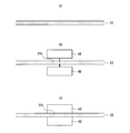
- a region for reducing the crystal grains is pressed.
- a tab 22 having uniform crystal grains throughout is prepared (FIG. 3A).
- region which makes a crystal grain small is mechanically pressed with the press machine 40 (FIG.3 (b), (c)).
- region to press-process is made to become an at least one part area
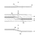
- a bent portion 22 a is formed on the tab 22.
- the bent portion 22 a can be formed by pressing a corresponding portion of the tab 22.
- the tab 22 having the region 22b in which the crystal grains are reduced as described above is prepared (FIG. 4A).
- the tab 22 is pressed by the press machine 44 to form the bent portion 22a (FIG. 4B).
- the bent portion 22 a is formed so that the region 22 b in which the crystal grains are reduced is located in the peripheral region of the solar battery cell 20.
- the bent portion 22a is formed in the tab 22 (FIG. 4C).
- the grain size of the crystal grains around the bent portion can be reduced by repeating the press forming to form the bent portion.
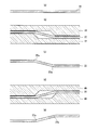
- a tab 22 having uniform crystal grains throughout is prepared (FIG. 5A).
- the tab 22 is pressed by the press machine 44 to form the bent portion 22a (FIGS. 5B and 5C).
- the tab 22 is plastically deformed to form the bent portion 22a, and the crystal grains in the area around the bent portion 22a are reduced.
- press working is performed so as to bend the bent portion 22a in the opposite direction (FIGS. 5D and 5E).
- the convex side of the bent portion 22a formed in FIG. 5B is pressed so that it becomes a concave surface in FIG. 5D, and the concave surface becomes a convex surface in FIG. 5D. Processing. By repeating such pressing, the crystal grains in the peripheral region of the bent portion 22a are made smaller.
- the tab 22 in which the crystal grains are made smaller in the peripheral region of the solar battery cell 20 than in other regions can be formed.
- the solar battery cell 20 can be formed by applying a conventional manufacturing method, and therefore a wiring method using the tab 22 which is a characteristic part will be described.
- the adhesive 24 is disposed on the bus bars of the first electrode 20b and the second electrode 20c.
- the tab 22 is bonded to the first electrode 20b and the second electrode 20c, and the adjacent solar cells 20 are connected.
- the bonding is performed so that the region where the crystal grains are smaller than the other region is located in the peripheral region of the solar battery cell 20. And it seals with the 1st protection member 26, the 2nd protection member 28, and the filler 30 as shown in FIG.6 (c).
Landscapes
- Photovoltaic Devices (AREA)
Priority Applications (1)
| Application Number | Priority Date | Filing Date | Title |
|---|---|---|---|
| PCT/JP2012/061421 WO2013161069A1 (fr) | 2012-04-27 | 2012-04-27 | Module de photopile et procédé de production d'un module de photopile |
Applications Claiming Priority (1)
| Application Number | Priority Date | Filing Date | Title |
|---|---|---|---|
| PCT/JP2012/061421 WO2013161069A1 (fr) | 2012-04-27 | 2012-04-27 | Module de photopile et procédé de production d'un module de photopile |
Publications (1)
| Publication Number | Publication Date |
|---|---|
| WO2013161069A1 true WO2013161069A1 (fr) | 2013-10-31 |
Family
ID=49482435
Family Applications (1)
| Application Number | Title | Priority Date | Filing Date |
|---|---|---|---|
| PCT/JP2012/061421 Ceased WO2013161069A1 (fr) | 2012-04-27 | 2012-04-27 | Module de photopile et procédé de production d'un module de photopile |
Country Status (1)
| Country | Link |
|---|---|
| WO (1) | WO2013161069A1 (fr) |
Cited By (1)
| Publication number | Priority date | Publication date | Assignee | Title |
|---|---|---|---|---|
| JP2014192367A (ja) * | 2013-03-27 | 2014-10-06 | Mitsubishi Electric Corp | 太陽電池モジュール及びその製造方法 |
Citations (6)
| Publication number | Priority date | Publication date | Assignee | Title |
|---|---|---|---|---|
| JP2000067642A (ja) * | 1998-08-27 | 2000-03-03 | Hitachi Cable Ltd | フラットケーブル用導体 |
| JP2002343994A (ja) * | 2001-05-11 | 2002-11-29 | Mitsubishi Electric Corp | 太陽電池の製造方法及びその装置 |
| JP2004197197A (ja) * | 2002-12-20 | 2004-07-15 | Jfe Steel Kk | 加工性および耐リジング性に優れたフェライト系ステンレス鋼板およびその製造方法 |
| JP2005191125A (ja) * | 2003-12-24 | 2005-07-14 | Kyocera Corp | 太陽電池素子接続用接続タブ及び太陽電池モジュール並びに太陽電池モジュールの製造方法 |
| WO2010021301A1 (fr) * | 2008-08-22 | 2010-02-25 | 三洋電機株式会社 | Module de cellules solaires |
| JP2011115833A (ja) * | 2009-12-07 | 2011-06-16 | Sumitomo Electric Ind Ltd | マグネシウム合金圧延板の矯正方法および矯正機、マグネシウム合金圧延板の製造方法 |
-
2012
- 2012-04-27 WO PCT/JP2012/061421 patent/WO2013161069A1/fr not_active Ceased
Patent Citations (6)
| Publication number | Priority date | Publication date | Assignee | Title |
|---|---|---|---|---|
| JP2000067642A (ja) * | 1998-08-27 | 2000-03-03 | Hitachi Cable Ltd | フラットケーブル用導体 |
| JP2002343994A (ja) * | 2001-05-11 | 2002-11-29 | Mitsubishi Electric Corp | 太陽電池の製造方法及びその装置 |
| JP2004197197A (ja) * | 2002-12-20 | 2004-07-15 | Jfe Steel Kk | 加工性および耐リジング性に優れたフェライト系ステンレス鋼板およびその製造方法 |
| JP2005191125A (ja) * | 2003-12-24 | 2005-07-14 | Kyocera Corp | 太陽電池素子接続用接続タブ及び太陽電池モジュール並びに太陽電池モジュールの製造方法 |
| WO2010021301A1 (fr) * | 2008-08-22 | 2010-02-25 | 三洋電機株式会社 | Module de cellules solaires |
| JP2011115833A (ja) * | 2009-12-07 | 2011-06-16 | Sumitomo Electric Ind Ltd | マグネシウム合金圧延板の矯正方法および矯正機、マグネシウム合金圧延板の製造方法 |
Cited By (1)
| Publication number | Priority date | Publication date | Assignee | Title |
|---|---|---|---|---|
| JP2014192367A (ja) * | 2013-03-27 | 2014-10-06 | Mitsubishi Electric Corp | 太陽電池モジュール及びその製造方法 |
Similar Documents
| Publication | Publication Date | Title |
|---|---|---|
| JPWO2013161069A1 (ja) | 太陽電池モジュール及び太陽電池モジュールの製造方法 | |
| JP4429306B2 (ja) | 太陽電池セル及び太陽電池モジュール | |
| JP5874011B2 (ja) | 太陽電池及び太陽電池モジュール | |
| CN108847425B (zh) | 太阳能电池模块 | |
| JP6624418B2 (ja) | 太陽電池モジュール | |
| US20100243024A1 (en) | Solar cell, solar cell module and solar cell system | |
| US20190123229A1 (en) | Solar cell module | |
| WO2013140552A1 (fr) | Module de cellules solaires | |
| US20170373210A1 (en) | Solar cell module | |
| JP5178489B2 (ja) | 太陽電池モジュール及びその製造方法 | |
| WO2017009957A1 (fr) | Module de batterie solaire et procédé de fabrication de module de batterie solaire | |
| JP5306353B2 (ja) | 太陽電池モジュール | |
| US20140190547A1 (en) | Solar cell module, and method for manufacturing solar cell module | |
| JP5999570B2 (ja) | 太陽電池モジュール及び太陽電池モジュールの製造方法 | |
| US20150083187A1 (en) | Solar cell module and solar cell module manufacturing method | |
| WO2013161069A1 (fr) | Module de photopile et procédé de production d'un module de photopile | |
| JP2015065303A (ja) | 太陽電池モジュール及びその製造方法 | |
| JP6032572B2 (ja) | 太陽電池モジュール及び太陽電池モジュールの製造方法 | |
| WO2013014810A1 (fr) | Module de batterie solaire et son procédé de fabrication | |
| JP5906422B2 (ja) | 太陽電池及び太陽電池モジュール | |
| JP2006278695A (ja) | 太陽電池モジュール | |
| JP6083685B2 (ja) | 太陽電池モジュール及び太陽電池モジュールの製造方法 | |
| WO2015118592A1 (fr) | Cellule solaire et procédé de fabrication de cellule solaire | |
| JP2024503612A (ja) | 電極アセンブリ | |
| JPWO2013114555A1 (ja) | 太陽電池モジュール及び太陽電池モジュールの製造方法 |
Legal Events
| Date | Code | Title | Description |
|---|---|---|---|
| 121 | Ep: the epo has been informed by wipo that ep was designated in this application |
Ref document number: 12875671 Country of ref document: EP Kind code of ref document: A1 |
|
| ENP | Entry into the national phase |
Ref document number: 2014512264 Country of ref document: JP Kind code of ref document: A |
|
| NENP | Non-entry into the national phase |
Ref country code: DE |
|
| 122 | Ep: pct application non-entry in european phase |
Ref document number: 12875671 Country of ref document: EP Kind code of ref document: A1 |