WO2013161129A1 - 電極箔及び電子デバイス - Google Patents
電極箔及び電子デバイス Download PDFInfo
- Publication number
- WO2013161129A1 WO2013161129A1 PCT/JP2012/083620 JP2012083620W WO2013161129A1 WO 2013161129 A1 WO2013161129 A1 WO 2013161129A1 JP 2012083620 W JP2012083620 W JP 2012083620W WO 2013161129 A1 WO2013161129 A1 WO 2013161129A1
- Authority
- WO
- WIPO (PCT)
- Prior art keywords
- electrode foil
- electrode
- layer
- foil
- light scattering
- Prior art date
- Legal status (The legal status is an assumption and is not a legal conclusion. Google has not performed a legal analysis and makes no representation as to the accuracy of the status listed.)
- Ceased
Links
Images






Classifications
-
- H—ELECTRICITY
- H05—ELECTRIC TECHNIQUES NOT OTHERWISE PROVIDED FOR
- H05B—ELECTRIC HEATING; ELECTRIC LIGHT SOURCES NOT OTHERWISE PROVIDED FOR; CIRCUIT ARRANGEMENTS FOR ELECTRIC LIGHT SOURCES, IN GENERAL
- H05B33/00—Electroluminescent light sources
- H05B33/12—Light sources with substantially two-dimensional [2D] radiating surfaces
- H05B33/26—Light sources with substantially two-dimensional [2D] radiating surfaces characterised by the composition or arrangement of the conductive material used as an electrode
-
- H—ELECTRICITY
- H10—SEMICONDUCTOR DEVICES; ELECTRIC SOLID-STATE DEVICES NOT OTHERWISE PROVIDED FOR
- H10F—INORGANIC SEMICONDUCTOR DEVICES SENSITIVE TO INFRARED RADIATION, LIGHT, ELECTROMAGNETIC RADIATION OF SHORTER WAVELENGTH OR CORPUSCULAR RADIATION
- H10F77/00—Constructional details of devices covered by this subclass
- H10F77/10—Semiconductor bodies
- H10F77/16—Material structures, e.g. crystalline structures, film structures or crystal plane orientations
- H10F77/169—Thin semiconductor films on metallic or insulating substrates
-
- H—ELECTRICITY
- H10—SEMICONDUCTOR DEVICES; ELECTRIC SOLID-STATE DEVICES NOT OTHERWISE PROVIDED FOR
- H10F—INORGANIC SEMICONDUCTOR DEVICES SENSITIVE TO INFRARED RADIATION, LIGHT, ELECTROMAGNETIC RADIATION OF SHORTER WAVELENGTH OR CORPUSCULAR RADIATION
- H10F77/00—Constructional details of devices covered by this subclass
- H10F77/40—Optical elements or arrangements
- H10F77/42—Optical elements or arrangements directly associated or integrated with photovoltaic cells, e.g. light-reflecting means or light-concentrating means
- H10F77/48—Back surface reflectors [BSR]
-
- H—ELECTRICITY
- H10—SEMICONDUCTOR DEVICES; ELECTRIC SOLID-STATE DEVICES NOT OTHERWISE PROVIDED FOR
- H10H—INORGANIC LIGHT-EMITTING SEMICONDUCTOR DEVICES HAVING POTENTIAL BARRIERS
- H10H20/00—Individual inorganic light-emitting semiconductor devices having potential barriers, e.g. light-emitting diodes [LED]
- H10H20/80—Constructional details
- H10H20/83—Electrodes
- H10H20/831—Electrodes characterised by their shape
-
- H—ELECTRICITY
- H10—SEMICONDUCTOR DEVICES; ELECTRIC SOLID-STATE DEVICES NOT OTHERWISE PROVIDED FOR
- H10K—ORGANIC ELECTRIC SOLID-STATE DEVICES
- H10K50/00—Organic light-emitting devices
- H10K50/80—Constructional details
- H10K50/85—Arrangements for extracting light from the devices
- H10K50/854—Arrangements for extracting light from the devices comprising scattering means
-
- H—ELECTRICITY
- H10—SEMICONDUCTOR DEVICES; ELECTRIC SOLID-STATE DEVICES NOT OTHERWISE PROVIDED FOR
- H10K—ORGANIC ELECTRIC SOLID-STATE DEVICES
- H10K77/00—Constructional details of devices covered by this subclass and not covered by groups H10K10/80, H10K30/80, H10K50/80 or H10K59/80
- H10K77/10—Substrates, e.g. flexible substrates
-
- H—ELECTRICITY
- H10—SEMICONDUCTOR DEVICES; ELECTRIC SOLID-STATE DEVICES NOT OTHERWISE PROVIDED FOR
- H10H—INORGANIC LIGHT-EMITTING SEMICONDUCTOR DEVICES HAVING POTENTIAL BARRIERS
- H10H20/00—Individual inorganic light-emitting semiconductor devices having potential barriers, e.g. light-emitting diodes [LED]
- H10H20/80—Constructional details
- H10H20/83—Electrodes
- H10H20/832—Electrodes characterised by their material
- H10H20/833—Transparent materials
-
- H—ELECTRICITY
- H10—SEMICONDUCTOR DEVICES; ELECTRIC SOLID-STATE DEVICES NOT OTHERWISE PROVIDED FOR
- H10H—INORGANIC LIGHT-EMITTING SEMICONDUCTOR DEVICES HAVING POTENTIAL BARRIERS
- H10H20/00—Individual inorganic light-emitting semiconductor devices having potential barriers, e.g. light-emitting diodes [LED]
- H10H20/80—Constructional details
- H10H20/83—Electrodes
- H10H20/832—Electrodes characterised by their material
- H10H20/835—Reflective materials
-
- H—ELECTRICITY
- H10—SEMICONDUCTOR DEVICES; ELECTRIC SOLID-STATE DEVICES NOT OTHERWISE PROVIDED FOR
- H10K—ORGANIC ELECTRIC SOLID-STATE DEVICES
- H10K30/00—Organic devices sensitive to infrared radiation, light, electromagnetic radiation of shorter wavelength or corpuscular radiation
- H10K30/80—Constructional details
- H10K30/87—Light-trapping means
-
- Y—GENERAL TAGGING OF NEW TECHNOLOGICAL DEVELOPMENTS; GENERAL TAGGING OF CROSS-SECTIONAL TECHNOLOGIES SPANNING OVER SEVERAL SECTIONS OF THE IPC; TECHNICAL SUBJECTS COVERED BY FORMER USPC CROSS-REFERENCE ART COLLECTIONS [XRACs] AND DIGESTS
- Y02—TECHNOLOGIES OR APPLICATIONS FOR MITIGATION OR ADAPTATION AGAINST CLIMATE CHANGE
- Y02E—REDUCTION OF GREENHOUSE GAS [GHG] EMISSIONS, RELATED TO ENERGY GENERATION, TRANSMISSION OR DISTRIBUTION
- Y02E10/00—Energy generation through renewable energy sources
- Y02E10/50—Photovoltaic [PV] energy
- Y02E10/52—PV systems with concentrators
-
- Y—GENERAL TAGGING OF NEW TECHNOLOGICAL DEVELOPMENTS; GENERAL TAGGING OF CROSS-SECTIONAL TECHNOLOGIES SPANNING OVER SEVERAL SECTIONS OF THE IPC; TECHNICAL SUBJECTS COVERED BY FORMER USPC CROSS-REFERENCE ART COLLECTIONS [XRACs] AND DIGESTS
- Y02—TECHNOLOGIES OR APPLICATIONS FOR MITIGATION OR ADAPTATION AGAINST CLIMATE CHANGE
- Y02E—REDUCTION OF GREENHOUSE GAS [GHG] EMISSIONS, RELATED TO ENERGY GENERATION, TRANSMISSION OR DISTRIBUTION
- Y02E10/00—Energy generation through renewable energy sources
- Y02E10/50—Photovoltaic [PV] energy
- Y02E10/549—Organic PV cells
-
- Y—GENERAL TAGGING OF NEW TECHNOLOGICAL DEVELOPMENTS; GENERAL TAGGING OF CROSS-SECTIONAL TECHNOLOGIES SPANNING OVER SEVERAL SECTIONS OF THE IPC; TECHNICAL SUBJECTS COVERED BY FORMER USPC CROSS-REFERENCE ART COLLECTIONS [XRACs] AND DIGESTS
- Y10—TECHNICAL SUBJECTS COVERED BY FORMER USPC
- Y10T—TECHNICAL SUBJECTS COVERED BY FORMER US CLASSIFICATION
- Y10T428/00—Stock material or miscellaneous articles
- Y10T428/12—All metal or with adjacent metals
- Y10T428/12993—Surface feature [e.g., rough, mirror]
-
- Y—GENERAL TAGGING OF NEW TECHNOLOGICAL DEVELOPMENTS; GENERAL TAGGING OF CROSS-SECTIONAL TECHNOLOGIES SPANNING OVER SEVERAL SECTIONS OF THE IPC; TECHNICAL SUBJECTS COVERED BY FORMER USPC CROSS-REFERENCE ART COLLECTIONS [XRACs] AND DIGESTS
- Y10—TECHNICAL SUBJECTS COVERED BY FORMER USPC
- Y10T—TECHNICAL SUBJECTS COVERED BY FORMER US CLASSIFICATION
- Y10T428/00—Stock material or miscellaneous articles
- Y10T428/24—Structurally defined web or sheet [e.g., overall dimension, etc.]
- Y10T428/24355—Continuous and nonuniform or irregular surface on layer or component [e.g., roofing, etc.]
-
- Y—GENERAL TAGGING OF NEW TECHNOLOGICAL DEVELOPMENTS; GENERAL TAGGING OF CROSS-SECTIONAL TECHNOLOGIES SPANNING OVER SEVERAL SECTIONS OF THE IPC; TECHNICAL SUBJECTS COVERED BY FORMER USPC CROSS-REFERENCE ART COLLECTIONS [XRACs] AND DIGESTS
- Y10—TECHNICAL SUBJECTS COVERED BY FORMER USPC
- Y10T—TECHNICAL SUBJECTS COVERED BY FORMER US CLASSIFICATION
- Y10T428/00—Stock material or miscellaneous articles
- Y10T428/24—Structurally defined web or sheet [e.g., overall dimension, etc.]
- Y10T428/24355—Continuous and nonuniform or irregular surface on layer or component [e.g., roofing, etc.]
- Y10T428/24364—Continuous and nonuniform or irregular surface on layer or component [e.g., roofing, etc.] with transparent or protective coating
Definitions
- the present invention relates to an electrode foil using a metal foil and an electronic device such as a light emitting element and a photoelectric element using the same.
- organic EL lighting In recent years, light-emitting elements such as organic EL lighting have attracted attention as environmentally friendly green devices.
- Features of organic EL lighting include 1) low power consumption compared to incandescent lamps, 2) thin and lightweight, and 3) flexibility.
- organic EL lighting is being developed to realize the features 2) and 3). In this regard, it is impossible to realize the characteristics 2) and 3) above with a glass substrate that has been conventionally used in flat panel displays (FPD) or the like.
- Ultra-thin glass is excellent in heat resistance, barrier properties, and light transmission properties, and has good flexibility, but handling properties are slightly inferior, thermal conductivity is low, and material cost is high.
- the resin film is excellent in handling properties and flexibility, has a low material cost, and has good light transmittance, but has poor heat resistance and barrier properties, and has low thermal conductivity.
- the metal foil has excellent characteristics such as excellent heat resistance, barrier properties, handling properties, thermal conductivity, good flexibility, and low material cost, except that it has no light transmittance.
- the thermal conductivity of a typical flexible glass or film is as low as 1 W / m ° C. or less, whereas in the case of a copper foil, it is as high as about 280 W / m ° C.
- Patent Document 1 Japanese Patent Laid-Open No. 2009-152113
- Patent Document 2 Japanese Patent Laid-Open No. 2008-243772 proposes that a nickel plating layer is provided on a metal substrate so that a smooth surface is formed without polishing and an organic EL element is formed thereon.
- Patent Document 3 Japanese Patent Application Laid-Open No.
- Patent Document 4 International Application No. 2011/152091
- Patent Document 5 International Application No. 2011/152092
- the arithmetic average roughness Ra is extremely low as 10.0 nm or less. It has been proposed to use a metal foil having a surface as a supporting substrate and electrode.
- a microlens or the like is disposed on the surface of the substrate on the light extraction side. Attempts have been made to improve luminous efficiency.
- formation of a microlens or the like is not advantageous from the viewpoint of productivity and cost because fine processing is required, and therefore, it is difficult to say that it is suitable for increasing the area.
- Inventors of the present invention by imparting a specific surface profile with a concave advantage to the surface of the metal foil itself, prevents short-circuiting between electrodes when used in electronic devices such as light-emitting elements and photoelectric elements.
- an electrode foil capable of exhibiting excellent light scattering properties was obtained, and it was found that the electrode foil itself can improve luminous efficiency and power generation efficiency.
- an object of the present invention is to provide an electrode foil capable of exhibiting excellent light scattering properties while preventing a short circuit between the electrodes.
- an electrode foil comprising a metal foil having a thickness of 1 to 250 ⁇ m, wherein at least one outermost surface of the electrode foil is 181 ⁇ m ⁇ 136 ⁇ m in accordance with JIS B 0601-2001.
- an electrode foil comprising a light scattering surface having a Pv / Pp ratio of 2.0 or more of the maximum valley depth Pv of the cross-sectional curve to the maximum peak height Pp of the cross-sectional curve measured with respect to the rectangular region of Is done.
- the electrode foil A semiconductor functional layer having semiconductor characteristics, provided on the light scattering surface of the electrode foil; An electronic device is provided.
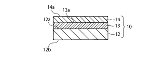
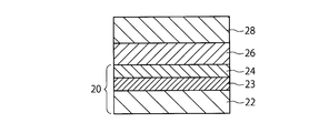
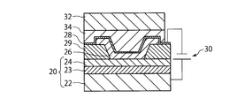
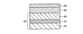
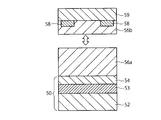
- FIG. 1 It is a schematic cross section which shows an example of the electrode foil by this invention. It is a schematic cross section which shows an example of the organic EL element which used the electrode foil by this invention as an anode. It is a schematic cross section which shows an example of the top emission type organic EL illumination by this invention. It is a schematic cross section which shows an example of the organic EL element which used the electrode foil by this invention as a cathode. It is a figure explaining an example of the lamination
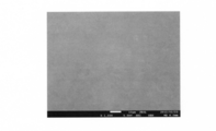
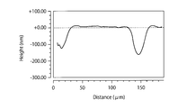
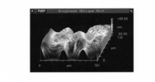
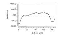
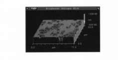
- FIG. 8 It is the image which observed the surface of the sample 6 shown by FIG. 8 by SEM (1000 times). It is the surface three-dimensional profile obtained by measuring the surface of the sample 6 shown by FIG. 8 with a non-contact surface shape measuring machine. It is the surface profile obtained by measuring the surface of the sample 6 shown by FIG. 8 with a non-contact surface shape measuring machine. It is the surface three-dimensional profile obtained by measuring the surface of the sample 7 shown by FIG. 8 with a non-contact surface shape measuring machine. It is the surface profile obtained by measuring the surface of the sample 7 shown by FIG. 8 with a non-contact surface shape measuring machine.
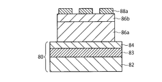
- FIG. 6 is a schematic cross-sectional view showing a layer configuration of a photoelectric element manufactured in Example 3.
- FIG. It is a figure which shows the relationship between the voltage measured with respect to the photoelectric element in Example 3, and an electric current. It is the image which observed the surface of the sample 8 produced in Example 4 by SEM (1000 times). It is the surface three-dimensional profile obtained by measuring the surface of the sample 8 shown by FIG. 16 with a non-contact surface shape measuring machine. It is the surface profile obtained by measuring the surface of the sample 8 shown by FIG. 16 with a non-contact surface shape measuring machine.
- FIG. 1 shows a schematic cross-sectional view of an example of an electrode foil according to the present invention.
- the electrode foil 10 shown in FIG. 1 has a metal foil 12 having a thickness of 1 to 250 ⁇ m.
- the electrode foil 10 may include a reflective layer 13 provided on one or both surfaces of the metal foil 12 directly or via a diffusion prevention layer as desired.
- the electrode foil 10 may include a buffer layer 14 provided directly on at least one surface or both surfaces of the metal foil 12 or the surface of the reflective layer 13 (if present) as desired.
- the electrode foil of the present invention is not limited to this, and has a one-layer configuration of the metal foil 12.
- the metal foil 12 There may be a two-layer structure of the metal foil 12 and the reflective layer 13. Alternatively, a five-layer configuration in which the reflective layer 13 and the buffer layer 14 are provided on both surfaces of the metal foil 12 may be employed.
- At least one outermost surface of the electrode foil 10 has a maximum valley depth Pv of the cross-sectional curve with respect to a maximum peak height Pp of the cross-sectional curve measured with respect to a rectangular area of 181 ⁇ m ⁇ 136 ⁇ m according to JIS B 0601-2001.
- a light scattering surface having a Pv / Pp ratio of 2.0 or more is provided.
- the maximum peak height Pp represents the height of the convex portion, while the maximum valley depth Pv represents the depth of the concave portion. Therefore, a Pv / Pp ratio of 2.0 or more means a specific surface profile having a concave portion preferentially over a convex portion.
- the electrode foil itself can exhibit excellent light scattering properties.
- the luminous efficiency and power generation efficiency can be improved with the electrode foil itself. This is because light is scattered due to the preferentially formed concave portions, and the formation of the convex portions is suppressed, thereby causing a short circuit between the electrodes (specifically, a short circuit with the counter electrode or between the semiconductor functional layers). This is thought to be due to prevention of short circuit.
- a preferable Pv / Pp ratio is 2.3 or more, more preferably 2.5 or more, still more preferably 2.8 or more, and particularly preferably 3.0 or more.
- the maximum peak height Pp and the maximum valley depth Pv can be measured in accordance with JIS B 0601-2001 using a commercially available non-contact surface shape measuring machine.
- the light scattering surface of the electrode foil 10 is the surface of the metal foil 12 in the case of a single layer configuration, and the outermost reflective layer 13 in the case of a multi-layer configuration including the reflective layer 13 and the buffer layer 14. Or the surface of the buffer layer 14 is meant.
- the above Pv / Pp ratio is realized by changing the Pv / Pp ratio of the surface 12a of the metal foil 12 on which the reflective layer 13 and / or the buffer layer 14 are formed as described above. Range, that is, 2.0 or more, preferably 2.3 or more, more preferably 2.5 or more, further preferably 2.8 or more, particularly preferably 3.0 or more, most preferably 3.3 or more.
- the reflective layer 13 and / or the buffer layer 14 can be formed thereon.
- a Pv / Pp ratio equal to or slightly higher than the arithmetic average roughness Pv / Pp ratio to be imparted on the outermost surface is imparted to the surface of the lower layer or foil.
- the evaluation of the Pv / Pp ratio of the surface of the metal foil that does not constitute the outermost surface due to the laminated state is made by creating a cross section from the surface of the metal foil by FIB (Focused Ion Beam) processing, The evaluation of the Pv / Pp ratio on the surface of the reflective layer that does not constitute the outermost surface due to the laminated state can be performed in the same manner.
- the light scattering surface of the electrode foil 10 preferably has innumerable recesses having a depth of 1 ⁇ m or less (typically 0.1 to 1 ⁇ m) and a major axis diameter of 100 ⁇ m or less (typically 1 to 100 ⁇ m).
- a depth typically 0.1 to 1 ⁇ m
- a major axis diameter typically 100 ⁇ m or less
- 200 or less (typically 1 to 200) of such recesses exist in a 10,000 ⁇ m 2 region.
- the metal foil 12 as an electrode as well as a supporting substrate, an electrode foil having the functions of a supporting substrate and an electrode can be provided.
- the thickness of the metal foil 12 is set to 1 to 250 ⁇ m, it can be used as an electrode that also serves as a supporting substrate for a flexible electronic device.
- the electrode foil 12 of the present invention is based on a metal foil, so that a support base material is not particularly required, for example, roll-to-roll. It can be manufactured efficiently by the process.
- the roll-to-roll process is an extremely advantageous process for efficiently mass-producing electronic devices in which a long foil wound in a roll shape is drawn out and subjected to a predetermined process and then wound up again.
- the electrode foil of this invention can make a support base material and a reflection layer unnecessary. For this reason, it is preferable that the electrode foil of this invention does not have an insulating layer in the part by which an electronic device is constructed
- the metal foil 12 is not particularly limited as long as it is a foil-like metal material having strength as a supporting substrate and electrical characteristics necessary as an electrode.
- a preferred metal foil is a nonmagnetic metal foil from the viewpoint of preventing adhesion of particulate matter generated during processing due to magnetism.
- Preferred examples of the nonmagnetic metal include copper, aluminum, nonmagnetic stainless steel, titanium, tantalum, and molybdenum, and more preferred are copper, aluminum, and nonmagnetic stainless steel.
- the most preferred metal foil is a copper foil. Copper foil is excellent in strength, flexibility, electrical characteristics and the like while being relatively inexpensive.
- the light scattering surface of the electrode foil 10 is preferably an ultra flat surface having an arithmetic average roughness Ra of 60.0 nm or less, more preferably 30.0 nm or less, still more preferably 20.0 nm or less, particularly preferably 10 It is 0.0 nm or less, more preferably 7.0 nm or less, and the roughness may be appropriately determined according to the application and performance required for the electrode foil.
- the lower limit of the arithmetic average roughness Ra is not particularly limited and may be zero. However, in consideration of the efficiency of the flattening process, 0.5 nm is cited as a guideline for the lower limit value.
- This arithmetic average roughness Ra can be measured using a commercially available roughness measuring device in accordance with JIS B 0601-2001.
- the light scattering surface of the electrode foil 10 is the surface of the metal foil 12 in the case of a single layer configuration, and is the outermost reflective layer in the case of a multi-layer configuration including the reflective layer 13 and the buffer layer 14. 13 or the surface of the buffer layer 14.
- realization of the said arithmetic mean roughness Ra in the case of such a multi-layer structure is the arithmetic mean roughness Ra of the surface 12a of the metal foil 12 in which the reflective layer 13 and / or the buffer layer 14 are formed.
- the reflection layer 13 and / or the buffer layer 14 can be formed thereon.
- an arithmetic average roughness Ra that is equal to or slightly smaller than the arithmetic average roughness Ra to be applied on the outermost surface is provided on the surface of the lower layer or foil.
- the arithmetic average roughness Ra of the surface of the metal foil that does not constitute the outermost surface due to the laminated state is evaluated by creating a cross section from the surface of the metal foil by FIB (Focused Ion Beam) processing, and using the transmission electron microscope (TEM), and the arithmetic average roughness Ra of the reflective layer surface that does not constitute the outermost surface due to the laminated state can be evaluated in the same manner.
- FIB Flucused Ion Beam
- Such an ultra-flat surface is formed by CMP (Chemical Mechanical This can be realized by polishing the metal foil by a polishing process.
- the CMP treatment can be performed according to known conditions using a known polishing liquid and a known polishing pad.
- a preferable polishing liquid it contains about 0.1 to 10% by weight of one or more kinds of abrasive grains selected from ceria, silica, alumina, zirconia and the like, and rust prevention such as benzotriazole (BTA).
- a preferable polishing pad includes a urethane pad.
- the polishing conditions are not particularly limited as long as the pad rotation speed, work load, polishing liquid application flow rate, etc. are adjusted appropriately, but the rotation speed is in the range of 20 to 1000 rpm, and the work load is in the range of 100 to 500 gf / cm 2 . In addition, it is preferable to adjust the polishing liquid application flow rate within the range of 20 to 200 cc / min.
- the ultra-flat surface 12a of the metal foil 12 can also be realized by polishing the metal foil 12 using an electrolytic polishing method, a buff polishing method, a chemical polishing method, or a combination thereof.
- the chemical polishing method is not particularly limited as long as the chemical solution, the chemical solution temperature, the chemical solution immersion time, etc. are appropriately adjusted.
- the chemical polishing of copper foil uses a mixture of 2-aminoethanol and ammonium chloride. Can be performed.
- the temperature of the chemical solution is preferably room temperature, and it is preferable to use an immersion method (Dip method). Further, since the chemical solution immersion time tends to deteriorate the flatness as it becomes longer, it is preferably 10 to 120 seconds, and more preferably 30 to 90 seconds.
- the metal foil after chemical polishing is preferably washed with running water. According to such a planarization process, it is possible to planarize a surface having a Ra arithmetic average roughness Ra of about 12 nm to Ra 10.0 nm or less, for example, about 3.0 nm.
- the ultra-flat surface 12a may be realized by a method of polishing the surface of the metal foil 12 by blasting, a method of rapidly cooling the surface of the metal foil 12 by melting it by a technique such as laser, resistance heating, or lamp heating. it can.
- the ultra-flat surface 12a obtained as described above cannot normally have a Pv / Pp ratio of 2.0 or more. Therefore, it is preferable to perform a process for imparting a Pv / Pp ratio of 2.0 or more to the ultra flat surface 12a.
- Preferable examples of such surface treatment include ultrasonic cleaning, chemical polishing using a chemical polishing liquid, and / or dry ice blasting.
- the ultrasonic cleaning can be performed, for example, by treating the surface of the metal foil for a predetermined time (for example, 10 minutes) with a predetermined high frequency output (for example, 60 W) using a commercially available flowing water type ultrasonic cleaning machine.
- a chemical polishing liquid for example, a polishing liquid for pure copper such as CPB-10 manufactured by Mitsubishi Gas Chemical Company
- the polishing liquid and water are mixed at a predetermined ratio (for example, a weight ratio of 1: 2). Then, it can be performed by immersing at room temperature for 1 minute, followed by washing with pure water, washing with dilute sulfuric acid (for example, 0.1N dilute sulfuric acid), washing with pure water again, and drying.
- a chemical polishing liquid for example, a polishing liquid for pure copper such as CPB-10 manufactured by Mitsubishi Gas Chemical Company
- dilute sulfuric acid for example, 0.1N dilute sulfuric acid
- the dry ice blasting method uses, for example, a commercially available apparatus such as a dry ice snow system (manufactured by Air Water) to inject carbon dioxide gas compressed to a high pressure from a thin nozzle, thereby causing the carbon dioxide solidified at a low temperature to be obtained on the ultra flat surface 12a. This can be done by spraying.
- a commercially available apparatus such as a dry ice snow system (manufactured by Air Water) to inject carbon dioxide gas compressed to a high pressure from a thin nozzle, thereby causing the carbon dioxide solidified at a low temperature to be obtained on the ultra flat surface 12a.
- This can be done by spraying.
- the electrolytic copper foil is electrodeposited, it is also possible to control the surface shape of the electrolytic copper foil by appropriately adjusting the presence or absence and amount of addition of organic matter, chlorine and the like.
- post-treatment for example, ultrasonic cleaning, chemical polishing, dry ice blast treatment, CMP treatment, etc.
- the thickness of the metal foil 12 is not particularly limited as long as it is a thickness that can be handled alone as a foil without impairing flexibility, but is 1 to 250 ⁇ m, preferably 5 to 200 ⁇ m, more preferably 10 to The thickness is 150 ⁇ m, more preferably 15 to 100 ⁇ m, but the thickness may be appropriately determined according to the application and performance required for the electrode foil. Therefore, the upper limit of the thickness is particularly preferably 50 ⁇ m, 35 ⁇ m, or 25 ⁇ m when reduction of the amount of metal used or weight reduction is desired, while the lower limit of the thickness is 25 ⁇ m when strength is more desired. , 35 ⁇ m or 50 ⁇ m is particularly preferable. With such a thickness, it is possible to easily cut using a commercially available cutting machine.
- the metal foil 12 has no problems such as cracking and chipping, and has advantages such as less generation of particles during cutting.
- the metal foil 12 can have various shapes other than a quadrangle, for example, a circle, a triangle, a polygon, and can be cut and welded. It is also possible to manufacture an electronic device. In this case, it is preferable not to form a semiconductor functional layer at the cut portion or welded portion of the metal foil 12.
- the ultra flat surface 12a is preferably washed with an alkaline solution.
- an alkaline solution a known alkaline solution such as a solution containing ammonia, a sodium hydroxide solution, or a potassium hydroxide solution can be used.
- a preferred alkaline solution is a solution containing ammonia, more preferably an organic alkaline solution containing ammonia, and even more preferably a tetramethylammonium hydroxide (TMAH) solution.
- TMAH tetramethylammonium hydroxide
- a preferable concentration of the TMAH solution is 0.1 to 3.0 wt%.
- cleaning is performed at 23 ° C. for 1 minute using a 0.4% TMAH solution.
- a similar cleaning effect can be obtained by performing UV (Ultra Violet) treatment in combination with such alkaline solution cleaning or instead of alkaline solution cleaning.
- UV Ultra Violet
- an acidic cleaning solution such as dilute sulfuric acid.
- the acid cleaning it is possible to perform cleaning for 30 seconds using dilute sulfuric acid.
- the dry ice blasting method is a method of removing particles by spraying carbon dioxide, which has been solidified at a low temperature, onto the ultra-flat surface 12a by spraying carbon dioxide gas compressed to a high pressure from a thin nozzle. Unlike the wet process, this dry ice blasting method has the advantages that the drying process can be omitted and organic substances can be removed.
- the dry ice blasting method can be performed using a commercially available apparatus such as a dry ice snow system (manufactured by Air Water). However, when particles have already been removed by a process (for example, dry ice blasting) for imparting a Pv / Pp ratio of 2.0 or more to the ultra-flat surface 12a, this particle removal step can be omitted. .
- the reflective layer 13 may be provided on the ultra-flat surface of the metal foil 12 directly or via an antireflection layer described later.
- the reflective layer 13 is preferably composed of at least one selected from the group consisting of aluminum, aluminum-based alloys, silver, and silver-based alloys. These materials are suitable for the reflective layer because of their high light reflectivity, and also have excellent flatness when thinned.
- aluminum or an aluminum-based alloy is preferable because it is an inexpensive material.
- an aluminum alloy and a silver alloy those having a general alloy composition used as an anode or a cathode in a light emitting element or a photoelectric element can be widely used.
- Examples of preferable aluminum-based alloy compositions include Al—Ni, Al—Cu, Al—Ag, Al—Ce, Al—Zn, Al—B, Al—Ta, Al—Nd, Al—Si, Al—La, Examples include Al—Co, Al—Ge, Al—Fe, Al—Li, Al—Mg, and Al—Mn alloys. Any element constituting these alloys can be arbitrarily combined according to the required characteristics.
- Examples of preferable silver alloy compositions include Ag—Pd, Ag—Cu, Ag—Al, Ag—Zn, Ag—Mg, Ag—Mn, Ag—Cr, Ag—Ti, Ag—Ta, and Ag—Co.
- the thickness of the reflective layer 13 is not particularly limited, but preferably has a thickness of 30 to 500 nm, more preferably 50 to 300 nm, and still more preferably 100 to 250 nm.
- the reflective layer 13 When the reflective layer 13 is composed of an aluminum film or an aluminum alloy film, the reflective layer may be composed of a laminated structure composed of at least two layers.
- the reflective layer 13 has a laminated structure of two layers partitioned by an interface, and the lower layer and the upper layer have different crystal orientations with the interface as a boundary. This effectively suppresses the thermal migration that can occur from the interface between the copper foil and the aluminum-containing reflective layer, even when the electrode foil is exposed to a considerably high temperature, resulting in surface flatness caused by thermal migration. It is possible to suppress a decrease in property and reflectance. That is, the heat resistance of the electrode foil can be improved.
- this aspect is particularly effective in the heat treatment after coating the hole injection layer performed at a temperature of 200 ° C. or higher, preferably 230 ° C. or higher, more preferably 250 ° C. or higher.
- Such an improvement in heat resistance is considered to be realized by preventing thermal migration that proceeds with priority given to crystal grain boundaries by an interface where the crystal grain boundaries become discontinuous.
- the number of interfaces in the reflective layer 13 may be two or more. In this case, the reflective layer has a laminated structure of three or more layers.
- the reflective layer having a multilayer structure can be manufactured by performing a film forming process such as sputtering a plurality of times at predetermined intervals.
- a film forming process such as sputtering a plurality of times at predetermined intervals.
- Preferred examples of such a method include the following. (1) The lower layer is preferably formed by sputtering until the thickness becomes 10 nm or more, and the sputtering is temporarily stopped. In this state, the lower layer is left in the chamber of the sputtering apparatus. This standing time is preferably 30 seconds or longer. Next, sputtering is resumed to form an upper layer. (2) The lower layer is preferably formed by sputtering until the thickness becomes 10 nm or more, and the sputtering is temporarily stopped. Then, the lower layer is brought into contact with the atmosphere.
- the metal foil on which the lower layer is formed may be taken out of the chamber of the sputtering apparatus and exposed to the atmosphere, or the chamber may be released to the atmosphere without taking out the metal foil.
- sputtering is resumed to form an upper layer.
- the time for exposing the lower layer to the atmosphere is about several seconds, and the desired effect can be obtained at the humidity and temperature as in a normal clean room environment.
- the lower layer is preferably formed by sputtering until the thickness becomes 10 nm or more, and the sputtering is temporarily stopped.
- oxygen is introduced into the chamber of the sputtering apparatus to form an oxygen atmosphere, and then vacuum is again applied to form an upper layer.
- the pressure in the chamber into which oxygen is introduced is preferably 0.01 Pa or more, more preferably 0.1 Pa or more, and further preferably 1 Pa or more.
- one interface is sufficient. Even one interface exhibits sufficient heat resistance at a high temperature of about 250 ° C. However, the heat resistance may be further improved by increasing the number of film formation processes and providing two or more interfaces.
- the diffusion prevention layer provided between the metal foil 12 and the reflection layer 13 as required may be any layer having a function of preventing the diffusion of the metal derived from the metal foil, and films of any known composition and structure are adopted. Is possible. This effectively suppresses the thermal migration that can occur from the interface between the copper foil and the aluminum-containing reflective layer, even when the electrode foil is exposed to a considerably high temperature, resulting in surface flatness caused by thermal migration. It is possible to suppress a decrease in property and reflectance. That is, the heat resistance of the electrode foil can be improved. Therefore, it can be said that this aspect is particularly effective in the heat treatment after coating the hole injection layer performed at a temperature of 200 ° C. or higher, preferably 230 ° C. or higher, more preferably 250 ° C. or higher. Note that the diffusion prevention layer may have a laminated structure of two or more layers.
- Preferred materials constituting the diffusion prevention layer include (i) refractory metals such as Mo, Ti, Ta, Cr and W, alloys and nitrides thereof, and (ii) transition metals such as Ni, Fe and Co and alloys thereof. (Iii) Conductive amorphous carbon, conductive oxide, magnesium-based alloy, and fluoride used in the buffer layer.
- examples of the diffusion prevention layer include Mo, Ti, Ta, Cr, W, Ni, Fe, Co, C, Zn, Li, Y, indium oxide, tin oxide, zinc oxide, molybdenum oxide, gallium oxide, vanadium oxide, tungsten oxide, ruthenium oxide, aluminum oxide, titanium oxide, titanium nitride, chromium nitride, tantalum nitride, NiP, Ni-Zn, LiF, MgF 2 , a layer comprising at least one selected from the group consisting of CaF 3 , NaAlF 6 , and NaF 6 . These compounds are not limited to the stoichiometric composition.
- the diffusion preventing layer For example, a substance in which oxygen in indium oxide (In 2 O 3 ) is partially deficient can be used as the diffusion preventing layer. It is. Thereby, thermal migration can be effectively prevented while the metal foil 12 and the reflective layer 13 are brought into close contact with each other electrically and mechanically. Formation of the diffusion preventing layer can be performed by various known methods such as sputtering, vacuum deposition, electrolytic plating, and electroless plating.
- the thickness of the diffusion preventing layer is not particularly limited as long as the effect of preventing metal diffusion required for the diffusion preventing layer is obtained, but is preferably 1 nm or more, more preferably 3 nm or more, and further preferably 5 nm or more. It is. Further, from the viewpoint of maintaining the surface flatness of the electrode foil, the thickness of the diffusion preventing layer is preferably 200 nm or less, and more preferably 100 nm or less.
- a buffer layer 14 is directly provided on at least one outermost surface of the metal foil 12 or the reflection layer 13 when present, and the surface of this buffer layer constitutes a light scattering surface.
- the buffer layer 14 is not particularly limited as long as it provides a desired work function in contact with the semiconductor functional layer.
- the buffer layer in the present invention is preferably transparent or translucent in order to ensure a sufficient light scattering effect.
- the buffer layer 14 is preferably at least one selected from a conductive amorphous carbon film, a conductive oxide film, a magnesium-based alloy film, and a fluoride film. What is necessary is just to select suitably according to the characteristic requested
- the conductive amorphous carbon film various amorphous carbon films imparted with conductivity by controlling the hydrogen concentration or impurity concentration can be used.
- the formation of the conductive amorphous carbon film is preferably performed by a sputtering method.
- a carbon target used for sputtering it is desirable to use a purified product. It is also possible to use porous carbon impregnated with B, Si, Al, Cu.
- a conductive amorphous carbon film is used as a buffer layer, any of an aluminum film, an aluminum-based alloy film, a silver film, and a silver-based alloy film is suitable as a reflective layer, but considering flatness and material cost Aluminum alloys are preferred.
- a preferable conductive amorphous carbon film is composed of conductive amorphous carbon having a hydrogen concentration of 15 at% or less.
- a more preferable hydrogen concentration is 12 at% or less, and further preferably 5 at% or less.
- the lower limit of the hydrogen concentration is not particularly limited and may be zero. However, considering the inevitable mixing of hydrogen due to the film formation environment during sputtering, 3 at% is an example of the lower limit.
- the hydrogen concentration in the buffer layer can be measured by various known methods, but is preferably performed by HFS (hydrogen forward scattering). In this specification, the hydrogen concentration in the conductive amorphous carbon film is defined as the hydrogen concentration when carbon and hydrogen are quantified with HFS or the like and the total number of these atoms is 100 at%.
- the conductive amorphous carbon is not substantially doped with impurities other than carbon and hydrogen.
- substantially undoped means that impurities are not intentionally doped in order to provide some function, and inevitably mixed due to the film forming environment during sputtering. Impurities are allowed.
- the conductive amorphous carbon in the present invention preferably has an oxygen concentration of 0 to 300 wtppm, a halogen element concentration of 0 to 1000 wtppm, and a nitrogen concentration of 0 to 500 wtppm.
- the thickness of the buffer layer 14 is not particularly limited, but is preferably 3 to 30 nm, more preferably 3 to 15 nm, and still more preferably 5 to 10 nm.
- Preferred InO x as the conductive oxide film SnO x, ZnO x, MoO x, GaO x, VO x, WO x, RuO x, 1 kind selected from the group consisting of AlO x, TiO x, and GeO x or
- a film composed of two or more kinds is exemplified, and typical examples include ITO (indium tin oxide) and IZO (indium zinc oxide).
- the conductive oxide film may be formed by a known method such as a sputtering method or a vacuum deposition method, and is preferably performed by a DC magnetron sputtering method.
- the target material used for the sputtering method can be manufactured by a hot press method or a cold press method, desired characteristics can be obtained by appropriately combining the above oxides.
- a conductive oxide film is used as the buffer layer, an Al—Ni alloy, Ag, or an Ag alloy is particularly suitable as the reflective layer.
- a preferable magnesium-based alloy film includes a film made of an alloy in which one or more selected from Ag, Al, Zn, Li, Y, and Ca are added to Mg.
- the magnesium-based alloy film may be formed by a known method such as a sputtering method or a vacuum deposition method, and is preferably performed by a vacuum deposition method.
- a preferable fluoride film includes a film composed of one or more selected from LiF, MgF 2 , CaF 2 , AlF 3 , Na 3 AlF 6 and NaF 6 .
- the fluoride film may be formed by a known method such as a sputtering method or a vacuum deposition method, and is preferably performed by a vacuum deposition method.
- An oxide film (not shown) may exist between the reflective layer 13 and the buffer layer 14. This oxide film is typically formed by unavoidably oxidizing the anode layer with oxygen in the atmosphere. Such an oxide film is preferably as thin as possible, and a preferable thickness is 3.0 nm or less, and more preferably 1.5 nm or less. Such an oxide film may be removed by etching or the like.
- the thickness of the electrode foil according to the present invention is preferably 1 to 300 ⁇ m, more preferably 1 to 250 ⁇ m, still more preferably 5 to 200 ⁇ m, particularly preferably 10 to 150 ⁇ m, most preferably 15 to 100 ⁇ m.
- the thickness may be appropriately determined according to the use and performance required for the electrode foil. Therefore, the upper limit of the thickness is particularly preferably 50 ⁇ m, 35 ⁇ m, or 25 ⁇ m when reduction of the amount of metal used or weight reduction is desired, while the lower limit of the thickness is 25 ⁇ m when strength is more desired. , 35 ⁇ m or 50 ⁇ m is particularly preferable.
- the thicknesses of these electrode foils are all the same as the thickness of the metal foil 12 described above, but this is usually the thickness of the reflective layer 13 and / or the buffer layer 14 that may be formed on the metal foil 12. This is because the thickness of the metal foil 12 is small enough to be ignored.
- the electrode foil according to the present invention can be preferably used as an electrode for various electronic devices (that is, an anode or a cathode).
- the electrode foil of the present invention is particularly preferably used as an electrode for a flexible electronic device because it is generally low stress and easily bent, but may be used for an electronic device having poor flexibility or rigidity.
- Examples of such electronic devices include i) light emitting elements such as organic EL elements, organic EL lighting, organic EL displays, electronic paper, liquid crystal displays, inorganic EL elements, inorganic EL displays, and LED lighting.
- Photoelectric elements such as thin film solar cells, are preferably organic EL elements, organic EL lighting, organic EL displays, organic solar cells, dye-sensitized solar cells, more preferably ultrathin.
- organic EL lighting in that light emission with high luminance can be obtained.
- the electrode foil according to the present invention can be preferably used as an anode or a cathode of the organic solar battery. . That is, by appropriately selecting the type of the organic semiconductor functional layer to be laminated on the electrode foil according to the present invention according to a known technique, the organic device can be configured as either an organic EL element or an organic solar battery.
- the electrode foil of the present invention may have both sides as light scattering surfaces, in which case it is advantageous to provide an electronic device on both sides of the electrode foil, thereby providing a double-sided functional element or a double-sided functional element provided with the electronic device on both sides.
- a foil can be provided. It is also possible to form a light emitting element on one side of the same electrode and a power generating element on the other side, thereby creating an unprecedented composite electronic device having both the function of an organic EL element and the function of an organic solar cell. It can also be produced.
- the electrode foil according to the present invention can be used not only for electrodes of organic EL elements but also for LED mounting substrates.
- the electrode foil according to the present invention can be preferably used as an anode or a cathode for LED illumination in that LED elements can be densely mounted.
- the length of the electrode foil according to the present invention is not particularly limited, but preferably has a certain length for application to a roll-to-roll process.
- the preferred length of the electrode foil varies depending on the specifications of the apparatus, etc., but is generally about 2 m or more. From the viewpoint of improving productivity, it is more preferably 20 m or more, further preferably 50 m or more, and particularly preferably 100 m or more. Most preferably, it is 1000 m or more.
- the preferred width of the electrode foil varies depending on the specifications of the apparatus, etc., but is generally 150 mm or more, and preferably 350 mm or more, more preferably 600 mm or more, and particularly preferably 1000 mm or more from the viewpoint of improving productivity. It is.
- wound which may be generated by winding can be prevented effectively. That is, as a measure to prevent scratches due to winding, it is effective to sandwich a material having higher elasticity than the electrode foil, such as a film, an embossed film, between the front and back surfaces, but when moving to the next process etc. Since the interlayer material needs to be wound, the handling becomes complicated. In this respect, the electrode foil whose both surfaces are light scattering layers can prevent scratches caused by winding without sandwiching such a material.
- an electronic device provided with a semiconductor functional layer having semiconductor characteristics on the light scattering surface of the electrode foil can be provided.
- the semiconductor functional layer is preferably formed directly on the light scattering surface.
- the semiconductor functional layer may be of any configuration or material as long as it has a semiconductor characteristic capable of exhibiting a desired function on or between electrodes, but it is an organic semiconductor, an inorganic semiconductor, or a mixture or combination thereof. It is preferable that it contains.
- the semiconductor functional layer has a function of excitation light emission or light excitation power generation, whereby the electronic device functions as a light emitting element or a photoelectric element.
- a transparent or translucent counter electrode is provided on the semiconductor functional layer.
- the electrode foil of the present invention is preferably applicable to a process in which a polymer material or a low molecular weight material is dissolved in a solvent such as chlorobenzene and applied in forming a semiconductor functional layer, and an in-line vacuum process is also applicable. It is suitable for improving productivity.
- the semiconductor functional layer may be provided on both sides of the electrode foil.
- the semiconductor functional layer is provided directly on the light scattering surfaces on both sides of the electrode foil, and one of the semiconductor functional layers has the same function as the other of the semiconductor functional layers. If it is set as the structure which gives the same function to both surfaces of an electrode foil, compared with the case where a function is provided only to one side, a significant functional improvement can be expected.
- the light emitting element can emit light in all directions, and the photoelectric element can obtain a higher voltage.
- the semiconductor functional layer is provided directly on the light scattering surfaces on both sides of the electrode foil, and one of the semiconductor functional layers has a function different from that of the other of the semiconductor functional layers.
- generation of the element which gave another function on the front side and back surface side (for example, indoor side and the outer side) is also attained.
- a light emitting element on one surface of the same electrode and a power generating element on the other surface, an unprecedented composite electronic device having both the function of an organic EL element and the function of an organic solar cell is provided.
- FIG. 2 shows an example of a layer structure of a top emission type organic EL element using the electrode foil of the present invention as an anode.
- the organic EL element shown in FIG. 2 includes an electrode foil 20 as an anode provided with a metal foil 22, a reflective layer 23, and optionally a buffer layer 24, an organic EL layer 26 provided directly on the surface of the buffer layer 24, and an organic And a cathode 28 as a translucent electrode provided directly on the surface of the EL layer 26.
- the buffer layer 24 is preferably composed of a conductive amorphous carbon film or a conductive oxide film so as to be suitable as an anode.
- organic EL layer 26 various known EL layer configurations used for organic EL elements can be used. If desired, a hole injection layer and / or a hole transport layer, a light emitting layer, and an electron transport layer as required. In addition, the electron injection layer may be sequentially provided from the anode electrode foil 20 toward the cathode 28. As the hole injection layer, the hole transport layer, the light emitting layer, the electron transport layer, and the electron injection layer, layers having various known configurations and compositions can be appropriately used and are not particularly limited.
- FIG. 3 shows an example of a layer configuration of a top emission type organic EL lighting in which the organic EL element shown in FIG. 2 is incorporated.
- the organic EL element can be electrically connected to the power source 30 through the metal foil 22 of the anode electrode foil 20.
- a region of the surface of the buffer layer 24 that is not in contact with the organic EL layer 26 is covered with an interlayer insulating film 29.
- the interlayer insulating film 29 As the interlayer insulating film 29, a Si-based insulating film formed by CVD is preferable because it has a high barrier property against moisture and oxygen that cause deterioration of the organic layer, and more preferably a SiN-based insulating film.
- a more preferred interlayer insulating film is a SiNO insulating film in that the internal stress of the film is small and the flexibility is excellent.
- a sealing material 32 is provided above the cathode 28 so as to face the organic EL element, and a sealing resin 34 is filled between the sealing material 32 and the cathode 28 to form a sealing film 34.
- the sealing material 32 glass or a film can be used. In the case of glass, it can be directly bonded onto the sealing film 34 using a hydrophobic adhesive tape. In the case of a film, both surfaces and end surfaces can be covered with a Si-based insulating film. When a film having a high barrier property is developed in the future, it is possible to perform sealing without performing a coating treatment, and it is expected that the film has excellent mass productivity.
- a film is desirable from the viewpoint of imparting flexibility, but a desired performance is obtained by using a sealing material in which a film is bonded to a very thin glass having a thickness of 20 to 100 ⁇ m. It is also possible.
- cathodes used in top emission type organic EL elements can be used as the cathode 28, and since it is necessary to transmit light, it is not particularly limited as long as it is transparent or translucent. A low one is preferred.
- Preferred cathodes include conductive oxide films, magnesium-based alloy films, and fluoride films, and it is more preferable to combine these in two or more layers. These films can be the same as those described for the buffer layer of the electrode foil.
- a particularly preferable cathode has a two-layer structure in which a transparent oxide layer as a cathode layer made of a conductive oxide film is laminated with a semi-transmissive metal layer as a buffer layer made of a magnesium alloy film and / or a fluoride film.
- a transparent oxide layer as a cathode layer made of a conductive oxide film is laminated with a semi-transmissive metal layer as a buffer layer made of a magnesium alloy film and / or a fluoride film.
- the most preferred example is a cathode structure in which a transparent oxide layer (cathode layer) made of IZO (indium zinc oxide) and a semi-transmissive metal layer (buffer layer) made of Mg—Ag are laminated. Further, the cathode structure may include two or more transparent oxide layers and / or two or more semi-transmissive metal layers.
- the light generated in the organic EL layer 26 passes through the cathode 28, the sealing film 34, and the sealing material 32 and is emitted to the outside.
- assistant base material suitably in the back surface of the electrode foil 20 according to a usage form. Since this portion does not affect the light emission characteristics, the degree of freedom in material selection is high. For example, if resin films such as polyethylene terephthalate (PET), polyimide (PI), polycarbonate (PC), polyethersulfone (PES), and polyethernitrile (PEN) are used, the flexibility will not be impaired, so it is optimal. I can say that.
- PET polyethylene terephthalate
- PI polyimide
- PC polycarbonate
- PES polyethersulfone
- PEN polyethernitrile
- FIG. 4 shows an example of a layer structure of a top emission type organic EL element using the electrode foil of the present invention as a cathode.
- a cathode electrode foil 40 including a metal foil 42, a reflective layer 43, and a buffer layer 44, an organic EL layer 46 provided directly on the surface of the buffer layer 44, and an organic EL layer 46.
- an anode 48 as a counter electrode provided directly on the surface.
- the organic EL layer 46 can be configured in the same manner as the organic EL layer 26 shown in FIG. 2, and the buffer layer 44 can be configured in the same manner as the cathode 28 shown in FIG. It is preferably composed of a system alloy film, a fluoride film, or a combination of two or more layers thereof.
- a more preferable buffer layer 44 is a semi-transmissive metal layer made of a magnesium-based alloy film and / or a fluoride film.
- the organic EL element using the cathode electrode foil 40 shown in FIG. 4 is the same as the organic EL element using the anode electrode foil 20 shown in FIG. 26 corresponds to a configuration in which the stacking order from the anode side to the cathode side in the interior 26 is reversed.
- a magnesium alloy film or a fluoride film is formed as the buffer layer 44 of the cathode electrode foil 40 by sputtering or vapor deposition, while a conductive amorphous carbon, MoO 3 or V 2 O 5 film is vapor deposited as the anode 48. It is preferable to form by.
- a conductive amorphous carbon film is formed on the organic EL layer, it is preferable to use a vacuum deposition method in order to avoid plasma damage during sputtering.
- a photoelectric device can be constructed on the light scattering surface.
- a photoelectric element according to a preferred embodiment of the present invention includes an electrode foil, a photoexcitation layer as a semiconductor functional layer provided directly on the surface of the electrode foil, and a translucent electrode as a counter electrode provided directly on the surface of the photoexcitation layer. Become.
- As the photoexcitation layer various structures and materials known as semiconductor functional layers of photoelectric devices can be used.
- an organic solar cell can be configured by replacing the organic EL layer 26 shown in FIG. 2 with a known organic solar cell active layer.
- a hole transport layer PEDOT: PSS (30 nm)
- a p-type organic semiconductor functional layer for example, BP (benzoic acid)
- a buffer layer for example, carbon buffer layer
- a solar cell can be formed by sequentially laminating a layer (for example, Mg—Ag) and a transparent electrode layer (for example, IZO).
- a metal foil 52 for example, a copper foil
- a reflective layer 53 for example, an aluminum film
- an n-type semiconductor buffer layer 54 for example, ZnO, SnO 2 , TiO 2 .
- the layer 56a (for example, P3HT: PCBM), the hole transport layer 56b (for example, PEDOT: PSS), and the electrode 58 may be sequentially stacked to constitute a solar cell.
- a known material can be appropriately used as a material constituting each of these layers, and is not particularly limited.
- the electrode used for the organic solar cell may have the same material and structure as the electrode used for the organic EL element.
- the electrode foil of the present invention is expected to improve the power generation efficiency due to light confinement due to the cavity effect by providing the reflective layer.
- the photoexcitation layer includes a plurality of known functional layers, and the lamination may be performed by sequentially laminating each phase from the electrode foil toward the counter electrode, or the electrode foil.
- the first stacked portion on the side and the second stacked portion on the counter electrode side are separately manufactured, and then the first and second stacked portions are bonded to each other to obtain a photoelectric device having a desired photoexcitation layer Also good. For example, as shown in FIG.
- an electrode foil 50 including a blend layer 56a of a p-type organic semiconductor and an n-type organic semiconductor is produced as a first laminated portion, while a resin film 59 (for example, polyethernitrile (PEN) ))
- PEN polyethernitrile
- a second laminated portion on which the counter electrode 58 and the hole transport layer 56b are formed is separately formed, and the blend layer 56a and the hole transport layer 56b are bonded to each other to bond the first and second layers. You may laminate
- the electrode foil 50 is prepared as a first laminated portion, while the counter electrode 58, the hole transport layer 56b and the p-type are formed on a resin film 59 (for example, polyethernitrile (PEN)).
- PEN polyethernitrile
- a second laminated portion in which an organic semiconductor and an n-type organic semiconductor blend layer 56a are formed is separately formed, and the first and second laminated layers are bonded together by bonding the blend layer 56a and the hole transport layer 56b together.
- the portions may be laminated.
- Example 1 Measurement of light scattering effect in electrode foils having various Pv / Pp ratios (1) Preparation of samples Electrode foil samples 1 to 5 having various Pv / Pp ratios were prepared. At that time, the measurement method of the surface property of each sample was as follows.
- Sample 1-Comparison In order to obtain Sample 1 provided with a standard reflective film for comparison, an aluminum film having a thickness of 200 nm was formed as a reflective layer on the surface of a quartz substrate having an arithmetic average roughness Ra of 0.2 nm by a sputtering method. In this sputtering, an Al target having a purity of 99.99% is mounted on a magnetron sputtering apparatus (MSL-464, manufactured by Tokki Co., Ltd.) connected to a cryo pump, and then input power (DC): 1000 W (3.
- MSL-464 magnetron sputtering apparatus
- Sample 2 having a low Pv / Pp ratio for comparison was prepared as follows. First, as a metal foil, a commercially available electrolytic copper foil having a thickness of 35 ⁇ m (DFF (Dual Flat Foil) manufactured by Mitsui Metal Mining Co., Ltd.) was prepared. The arithmetic average roughness Ra of the copper foil surface was 16.5 nm. The surface of the copper foil substrate was chemically polished using a chemical polishing agent (CPB-10, manufactured by Mitsubishi Gas Chemical Company), which was diluted by mixing the chemical polishing agent and water at a weight ratio of 1: 2.
- the copper foil substrate was immersed in the solution for 1 minute at room temperature, and the copper foil substrate thus treated was washed with pure water, washed with 0.1N dilute sulfuric acid, and washed again with pure water.
- an aluminum reflective layer was formed under the same conditions as in Sample 1.
- the surface property of Sample 2 obtained was measured in the same manner as Sample 1. As a result, the arithmetic average roughness Ra is 19.3 nm.
- the Pv / Pp ratio was 1.86.
- Sample 3 having a Pv / Pp ratio within the scope of the present invention was prepared as follows. First, as the metal foil, a commercially available electrolytic copper foil having a thickness of 35 ⁇ m (DFF (Dual Flat Foil) manufactured by Mitsui Metal Mining Co., Ltd.) was prepared. The surface of this copper foil was subjected to CMP treatment using a polishing machine manufactured by MT Corporation. This CMP treatment was performed for 40 seconds under the conditions of pad rotation speed: 30 rpm, load: 200 gf / cm 2 , and liquid supply amount: 100 cc / min using a polishing pad with XY grooves and a colloidal silica-based polishing liquid.
- DFF Double Flat Foil
- the arithmetic average roughness Ra of the CMP-treated copper foil surface was 6.2 nm, and the copper foil surface was applied for 20 minutes at a high frequency output of 60 W using a flowing water type ultrasonic cleaner (manufactured by Honda Electronics Co., Ltd.).
- a flowing water type ultrasonic cleaner manufactured by Honda Electronics Co., Ltd.
- an aluminum reflective layer was formed under the same conditions as in Sample 1.
- the surface properties of Sample 3 thus obtained were measured.
- the average roughness Ra is 16.2 nm, Pv / Pp ratio was 2.14.
- Sample 4 having a Pv / Pp ratio within the scope of the present invention was prepared as follows. First, as the metal foil, a commercially available electrolytic copper foil having a thickness of 35 ⁇ m (DFF (Dual Flat Foil) manufactured by Mitsui Metal Mining Co., Ltd.) was prepared. The surface of this copper foil was subjected to CMP treatment using a polishing machine manufactured by MT Corporation. This CMP treatment was performed for 60 seconds under the conditions of pad rotation speed: 30 rpm, load: 200 gf / cm 2 , and liquid supply amount: 100 cc / min, using a polishing pad with XY grooves and a colloidal silica-based polishing liquid.
- DFF Double Flat Foil
- the arithmetic average roughness Ra of the CMP-treated copper foil surface was 3.1 nm, and the copper foil surface was applied for 10 minutes at a high frequency output of 60 W using a flowing water ultrasonic cleaner (manufactured by Honda Electronics Co., Ltd.).
- An aluminum reflective layer was formed on the polished and surface-modified surface under the same conditions as in Sample 1. The properties of the surface of Sample 4 thus obtained were measured.
- the average roughness Ra is 6.1 nm, Pv / Pp ratio was 2.54.
- Sample 4 having a Pv / Pp ratio within the scope of the present invention was prepared as follows. First, as the metal foil, a commercially available electrolytic copper foil having a thickness of 35 ⁇ m (DFF (Dual Flat Foil) manufactured by Mitsui Metal Mining Co., Ltd.) was prepared. The surface of this copper foil was subjected to CMP treatment using a polishing machine manufactured by MT Corporation. This CMP treatment was performed for 40 seconds under the conditions of pad rotation speed: 30 rpm, load: 200 gf / cm 2 , and liquid supply amount: 100 cc / min using a polishing pad with XY grooves and a colloidal silica-based polishing liquid.
- DFF Double Flat Foil
- the arithmetic average roughness Ra of the CMP-treated copper foil surface was 6.8 nm, and the surface of the copper foil was applied for 10 minutes with a high-frequency output of 60 W using a flowing water ultrasonic cleaner (manufactured by Honda Electronics Co., Ltd.).
- An aluminum reflective layer was formed on the polished and surface-modified surface under the same conditions as in Sample 1. The properties of the surface of Sample 5 thus obtained were measured.
- the average roughness Ra is 13.7 nm, Pv / Pp ratio was 4.9.
- the evaluation of the light scattering effect is made with respect to the reflection angles of 10 °, 30 °, and 60 °, where the positive absolute reflectance of sample 1 as a standard reflection film is 1, and the positive absolute reflectance of samples 2 to 5 is relatively
- the positive and absolute reflectance values of Samples 2 to 5 were measured, and a value obtained by dividing the value by the positive and absolute reflectance value of the standard reflective film (Sample 1) was calculated as a light scattering relative value. Therefore, the larger the light scattering relative value, the better the light scattering effect.
- the reflective layer of each sample is made of the same material (aluminum film having a purity of 99.99%) and substantially the same film thickness (200 nm ( ⁇ 5%)). The light absorption conditions caused by the thickness were made to match.
- the sample size was 80 mm ⁇ 80 mm square.
- the light scattering relative values obtained for each sample were as shown in Tables 1 to 3 below.
- Example 2 Production and Evaluation of Electrode Foil with Various Surface Properties
- An electrode foil was prepared.
- the light scattering characteristics of these electrode foils were evaluated in the same manner as in Example 1, as shown in FIG. 8, the light scattering characteristics of all samples having a Pv / Pp ratio of 2.0 or more were improved by 1.2 times.
- samples having a Pv / Pp ratio of less than 2.0 did not have such a high light scattering property.
- a light emitting element or a power generation element was produced using these electrode foils, as shown in FIG.
- the surface profile shown in FIGS. 10 and 11 relates to the sample 6 in which the light scattering effect is improved according to the present invention, and is a desirable surface profile in which the formation of the convex portion is suppressed and the concave portion is formed preferentially.
- the surface profiles shown in FIGS. 12 and 13 relate to the sample 7 which was poor in improving the light scattering effect.
- Example 3 Evaluation of Photoelectric Characteristics (1) Production of Photoelectric Element As shown in FIG. 14, samples 6 and 7 having an aluminum reflective layer 83 on a copper foil 82 obtained as an electrode foil in Example 2 were used. Thus, a photoelectric element was manufactured. First, an n-type semiconductor buffer layer 84 made of ZnO and having a thickness of 20 nm was formed on the aluminum reflective layer 83 by sputtering. On the buffer layer 84, an interlayer insulating film made of silicon nitride was formed using a plasma CVD apparatus (manufactured by Samco, PD-2202L).
- a plurality of thin glasses having a thickness of 0.1 mm, a width of 2 mm, and a length of 10 mm were arranged on the electrode foil so as to have a width of 2 mm, thereby covering a portion to be a light receiving portion.
- the thin glass was removed. Thereafter, the electrode foil 80 was washed with an isopropyl alcohol solution heated to 40 to 50 ° C. and dried using nitrogen gas.
- PEDOT: PSS (poly (3,4-ethylenedioxythiophene / poly (4-styrenesulfonate)) dispersion (1.3 wt%) was spin coated on the electrode foil at 5000 rpm.
- the PEDOT: PSS layer 86b was obtained by drying on a hot plate for 30 minutes, and a counter electrode 88a was obtained by depositing gold so as to have a thickness of about 100 nm using a vacuum deposition apparatus.
- the portion that should become the light receiving portion was not shielded by using a comb-shaped metal mask, and was then baked in an inert atmosphere (nitrogen) at 150 ° C. for 30 minutes, as shown in FIG. A photoelectric element was obtained.
- the sample 6 with a high Pv / Pp ratio has a significantly higher fill factor FF and conversion efficiency ⁇ than the sample 7 with a low Pv / Pp ratio. It can be seen that is far superior.
- Example 4 Production and Evaluation of Electrode Foil Only for Concave Parts Sample 2 except that a commercially available electrolytic copper foil (Mitsui Metal Mining Co., Ltd., 3EC-III) with a thickness of 35 ⁇ m was used as the metal foil and the CMP treatment was performed for 2 minutes
- An electrode foil was prepared in the same manner as described above to obtain Sample 8.
- SEM SEM
- a surface property having substantially only concave portions was observed as shown in FIG.
- the surface profile was measured with the non-contact surface shape measuring machine (NewView5032, the product made by Zygo) about the sample 8, the profile image shown by FIG. 17 and 18 was obtained.
- the light scattering surface of the sample 8 had a highly desirable surface profile in which convex portions were substantially removed and only concave portions were formed.
- Most of the observed recesses had a depth of 1 ⁇ m or less and a longitudinal length of 100 ⁇ m or less.
- the number of the recesses was counted in the field of view of SEM 1000 times (10000 ⁇ m 2 ), it was about 170.
- it is possible to exhibit more excellent light scattering properties while more reliably preventing a short circuit between the electrodes, thereby improving luminous efficiency and The power generation efficiency can be further improved.
Landscapes
- Physics & Mathematics (AREA)
- Optics & Photonics (AREA)
- Electroluminescent Light Sources (AREA)
- Photovoltaic Devices (AREA)
- Electrodes Of Semiconductors (AREA)
- Led Devices (AREA)
Abstract
電極間の短絡を防止しながら、優れた光散乱性を発揮することが可能な電極箔が提供される。本発明の電極箔は、厚さ1~250μmの金属箔を備えてなり、電極箔の少なくとも一方の最表面に、JIS B 0601-2001に準拠して181μm×136μmの矩形領域に対して測定される、断面曲線の最大山高さPpに対する断面曲線の最大谷深さPvのPv/Pp比が2.0以上である光散乱面を備えてなる。
Description
この出願は、2012年4月23日に出願された日本国特許出願第2012-097854号に基づく優先権を主張するものであり、その全体の開示内容が参照により本明細書に組み込まれる。
本発明は、金属箔を用いた電極箔及びそれを用いた発光素子、光電素子等の電子デバイスに関するものである。
近年、有機EL照明等の発光素子が、環境に配慮したグリーンデバイスとして注目されている。有機EL照明の特徴としては、1)白熱灯に対して低消費電力であること、2)薄型かつ軽量であること、3)フレキシブルであることが挙げられる。現在、有機EL照明は、上記2)及び3)の特徴を実現すべく開発が進められている。この点、フラットパネルディスプレイ(FPD)等で従来使用されてきたガラス基板では、上記2)及び3)の特徴を実現することは不可能である。
そこで、有機EL照明のための支持体としての基板(以下、支持基材という)に対する研究が進められており、その候補として、極薄ガラス、樹脂フィルム、金属箔等が提案されている。極薄ガラスは、耐熱性、バリア性、及び光透過性に優れ、フレキシブル性も良好であるが、ハンドリング性がやや劣り、熱伝導性が低く、材料コストも高い。また、樹脂フィルムは、ハンドリング性及びフレキシブル性に優れ、材料コストも低く、光透過性も良好であるが、耐熱性及びバリア性に乏しく、熱伝導性が低い。
これに対し、金属箔は、光透過性が無いことを除けば、耐熱性、バリア性、ハンドリング性、熱伝導性に優れ、フレキシブル性も良好であり、材料コストも低いといった優れた特徴を有する。特に、熱伝導性については、典型的なフレキシブルガラスやフィルムが1W/m℃以下と極めて低いのに対し、銅箔の場合、280W/m℃程度と極めて高い。
金属基板を用いた発光素子を実現するために、特許文献1(特開2009-152113号公報)では金属基板の表面を研磨処理やメッキ処理により平滑化して、その上に有機層を形成することが提案されている。また、特許文献2(特開2008-243772号公報)では金属基板上にニッケルめっき層を設けることで研磨等をすることなく平滑面を形成し、その上に有機EL素子を形成することが提案されている。一方、金属基板を用いた光電素子も提案されており、例えば、特許文献3(特開2011-222819号公報)には平滑化処理された金属基材上に有機薄膜起電力層を設けた太陽電池が開示されている。これらの技術においては、電極間の短絡防止のため、金属基板表面の平滑化が重要な課題となっている。この課題に対処した技術として、特許文献4(国際出願第2011/152091号)及び特許文献5(国際出願第2011/152092号)では、算術平均粗さRaが10.0nm以下と極めて低い超平坦面を備えた金属箔を支持基材兼電極として用いることが提案されている。
ところで、発光素子や光電素子において、光を効率よく引き出す又は取り込むためには、金属箔上で光を散乱させた方が有利であることが知られている。すなわち、光散乱性が高いと、発光素子では発光効率が上がり、光電素子では発電効率が上がる。この点、通常の金属箔の表面で短絡を生じさせることなく光を十分に散乱させることは困難であるため、発光素子の場合には、光取り出し側の基板表面にマイクロレンズなどを配置して、発光効率を向上させる試みがなされている。しかしながら、マイクロレンズなどの形成は、微細加工が必要となることから生産性やコストの観点から有利とはいえず、それ故、大面積化に適しているとは言い難い。
本発明者らは、今般、金属箔の表面自体に凹部優位の特異的な表面プロファイルを付与することで、発光素子、光電素子等の電子デバイスに使用した際の電極間の短絡を防止しながら、優れた光散乱性を発揮することが可能な電極箔が得られ、それにより電極箔自体で発光効率や発電効率を向上できるとの知見を得た。
したがって、本発明の目的は、電極間の短絡を防止しながら、優れた光散乱性を発揮することが可能な電極箔を提供することにある。
本発明の一態様によれば、厚さ1~250μmの金属箔を備えてなる電極箔であって、 前記電極箔の少なくとも一方の最表面に、JIS B 0601-2001に準拠して181μm×136μmの矩形領域に対して測定される、断面曲線の最大山高さPpに対する断面曲線の最大谷深さPvのPv/Pp比が2.0以上である光散乱面を備えてなる、電極箔が提供される。
本発明の他の一態様によれば、
上記電極箔と、
前記電極箔の前記光散乱面上に設けられる、半導体特性を有する半導体機能層と、
を備えた、電子デバイスが提供される。
上記電極箔と、
前記電極箔の前記光散乱面上に設けられる、半導体特性を有する半導体機能層と、
を備えた、電子デバイスが提供される。
電極箔
図1に本発明による電極箔の一例の模式断面図を示す。図1に示される電極箔10は、厚さ1~250μmの金属箔12を有してなる。電極箔10は、所望により金属箔12の一方の面又は両面に直接、又は拡散防止層を介して設けられる反射層13を備えていてもよい。また、電極箔10は、所望により少なくとも金属箔12の一方の面若しくは両面又は(存在する場合には)反射層13の表面上に直接設けられるバッファ層14を備えていてもよい。図1に示される電極箔10は金属箔12、反射層13及びバッファ層14を備えた3層構成であるが、本発明の電極箔はこれに限定されず、金属箔12の1層構成であってもよいし、金属箔12及び反射層13の2層構成であってもよい。あるいは、金属箔12の両面に反射層13及びバッファ層14を備えた5層構成であってもよい。
図1に本発明による電極箔の一例の模式断面図を示す。図1に示される電極箔10は、厚さ1~250μmの金属箔12を有してなる。電極箔10は、所望により金属箔12の一方の面又は両面に直接、又は拡散防止層を介して設けられる反射層13を備えていてもよい。また、電極箔10は、所望により少なくとも金属箔12の一方の面若しくは両面又は(存在する場合には)反射層13の表面上に直接設けられるバッファ層14を備えていてもよい。図1に示される電極箔10は金属箔12、反射層13及びバッファ層14を備えた3層構成であるが、本発明の電極箔はこれに限定されず、金属箔12の1層構成であってもよいし、金属箔12及び反射層13の2層構成であってもよい。あるいは、金属箔12の両面に反射層13及びバッファ層14を備えた5層構成であってもよい。
電極箔10の少なくとも一方の最表面は、JIS B 0601-2001に準拠して181μm×136μmの矩形領域に対して測定される、断面曲線の最大山高さPpに対する断面曲線の最大谷深さPvのPv/Pp比が2.0以上である光散乱面を備えてなる。最大山高さPpは凸部の高さを表す一方、最大谷深さPvは凹部の深さを表す。したがって、2.0以上のPv/Pp比は、凹部を凸部よりも優先的に備えた特異的な表面プロファイルを意味する。そして、本発明者らの知見によれば、このような凹部優位の特異的な表面プロファイルを電極箔10に付与することにより、優れた光散乱性を電極箔自体に発揮させることができ、それにより電極箔自体で発光効率や発電効率を向上することができる。これは、優先的に形成される凹部に起因して光が散乱されるとともに、凸部の形成が抑制されることで電極間の短絡(具体的には対向電極との短絡や半導体機能層間における短絡)が防止されることによるものと考えられる。特に、本発明の電極箔にあっては、金属箔ないし電極箔の表面プロファイル自体で光散乱効果が得られるため、マイクロレンズ形成及びそれに伴う微細加工を不要として生産性やコスト効率の低下を回避することができ、それ故、大面積化にも適している。好ましいPv/Pp比は2.3以上であり、より好ましくは2.5以上、さらに好ましくは2.8以上、特に好ましくは3.0以上である。なお、最大山高さPp及び最大谷深さPvは、市販の非接触表面形状測定機を用いてJIS B 0601-2001に準拠して測定することができる。
ここで、電極箔10の光散乱面とは、1層構成の場合は金属箔12の表面となり、反射層13やバッファ層14を含む複数層構成の場合には最も外側に位置する反射層13又はバッファ層14の表面を意味する。もっとも、このような複数層構成の場合における上記Pv/Pp比の実現は、反射層13及び/又はバッファ層14が形成されることになる金属箔12の表面12aのPv/Pp比を上記同様の範囲、すなわち2.0以上、好ましくは2.3以上、より好ましくは2.5以上、さらに好ましくは2.8以上、特に好ましくは3.0以上、最も好ましくは3.3以上にしておき、その上に反射層13及び/又はバッファ層14を成膜することにより行うことができる。このように、最表面において付与されるべき算術平均粗さPv/Pp比と同等もしくは若干高めのPv/Pp比をそれよりも下の層ないし箔の表面に付与しておくのが好ましい。なお、積層状態のため最表面を構成しない金属箔表面のPv/Pp比の評価は、金属箔表面からFIB(Focused Ion Beam)加工にて断面を作製し、その断面を透過型電子顕微鏡(TEM)にて観察することにより行うことができ、積層状態のため最表面を構成しない反射層表面のPv/Pp比の評価も同様にして行うことができる。
電極箔10の光散乱面が、深さ1μm以下(典型的には0.1~1μm)で長軸径100μm以下(典型的には1~100μm)の凹部を無数に有するのが好ましく、それにより実質的に凸部を無くして顕著に高いPv/Pp比を実現することができる。深さが1μmより浅いとその上に形成される半導体機能層をより確実に支持することができる。また、長軸径が1μm以上であると光散乱効果を得やすくなる。このような凹部は10000μm2の領域内に200個以下(典型的には1~200個)存在するのが好ましい。
本発明にあっては、金属箔12を支持基材のみならず電極として用いることで、支持基材と電極の機能を兼ね備えた電極箔を提供することができる。その上、金属箔12の厚さを1~250μmとしたことで、フレキシブル電子デバイス用の支持基材を兼ねた電極として用いることができる。このようなフレキシブル電子デバイスの製造に関して、本発明の電極箔12は、金属箔をベースとしているため、支持基材を特に必要とすることなく、例えばロール・トゥ・ロール(roll-to-roll)プロセスによって効率的に製造することができる。ロール・トゥ・ロール・プロセスは、ロール状に巻いた長尺状の箔を引き出して所定のプロセスを施したのち再び巻き取るという電子デバイスを効率的に量産する上で極めて有利なプロセスであり、本願発明の用途である発光素子及び光電素子等の電子デバイスの量産化を実現する上で鍵になるプロセスである。このように、本発明の電極箔は、支持基材及び反射層を不要にすることができる。このため、本発明の電極箔は、少なくとも電子デバイスが構築される部分に絶縁層を有しないのが好ましく、より好ましくはいかなる部位にも絶縁層を有しない。
金属箔12は、支持基材としての強度及び電極として必要な電気的特性を有する箔状金属材料であれば特に限定されない。好ましい金属箔は、加工時に発生する粒子状物の帯磁による付着を防止できる観点から、非磁性金属箔である。非磁性金属の好ましい例としては、銅、アルミニウム、非磁性ステンレス、チタン、タンタル、モリブデン等が挙げられ、より好ましくは銅、アルミニウム、及び非磁性ステンレスである。最も好ましい金属箔は銅箔である。銅箔は比較的安価でありながら、強度、フレキシブル性、電気的特性等に優れる。
電極箔10の光散乱面は、60.0nm以下の算術平均粗さRaを有する超平坦面であるのが好ましく、より好ましくは30.0nm以下、さらに好ましくは20.0nm以下、特に好ましくは10.0nm以下、より特に好ましくは7.0nm以下であり、電極箔に求められる用途や性能等に応じて粗さを適宜決定すればよい。算術平均粗さRaの下限は特に限定されずゼロであってもよいが、平坦化処理の効率を考慮すると0.5nmが下限値の目安として挙げられる。この算術平均粗さRaは、JIS B 0601-2001に準拠して市販の粗さ測定装置を用いて測定することができる。
前述のとおり、電極箔10の光散乱面とは、1層構成の場合は金属箔12の表面となり、反射層13やバッファ層14を含む複数層構成の場合には最も外側に位置する反射層13又はバッファ層14の表面を意味する。もっとも、このような複数層構成の場合における上記算術平均粗さRaの実現は、反射層13及び/又はバッファ層14が形成されることになる金属箔12の表面12aの算術平均粗さRaを上記同様の範囲、すなわち60.0nm以下、好ましくは30.0nm以下、より好ましくは20.0nm以下、さらに好ましくは10.0nm以下、特に好ましくは7.0nm以下、最も好ましくは5.0nm以下にしておき、その上に反射層13及び/又はバッファ層14を成膜することにより行うことができる。このように、最表面において付与されるべき算術平均粗さRaよりも同等もしくは若干小さめの算術平均粗さRaをそれよりも下の層ないし箔の表面に付与しておくのが好ましい。なお、積層状態のため最表面を構成しない金属箔表面の算術平均粗さRaの評価は、金属箔表面からFIB(Focused Ion Beam)加工にて断面を作製し、その断面を透過型電子顕微鏡(TEM)にて観察することにより行うことができ、積層状態のため最表面を構成しない反射層表面の算術平均粗さRaの評価も同様にして行うことができる。
電極箔10の光散乱面の算術平均粗さRaが上述のごとく極めて小さいと、発光素子、光電素子等の電子デバイスに使用した際の電極間の短絡をより一層効果的に防止できる。
このような超平坦面は、CMP(Chemical Mechanical
Polishing)処理により金属箔を研磨することにより実現することができる。CMP処理は、公知の研磨液及び公知の研磨パッドを用いて、公知の条件に従って行うことができる。好ましい研磨液としては、セリア、シリカ、アルミナ、ジルコニア等から選択される1種以上の研磨砥粒約0.1~10重量%程度を含んでなり、かつ、ベンゾトリアゾール(BTA)等の防錆剤と、更に/又は、キナルシン酸、キノリン酸、ニコチン酸、リンゴ酸、アミノ酸、クエン酸、カルボン酸、ポリアクリル酸等の有機錯体形成剤と、カチオン性界面活性剤、アニオン性界面活性剤等の界面活性剤と、所望により防食剤とをさらに含むものが挙げられる。好ましい研磨パッドとしては、ウレタン製のパッドが挙げられる。研磨条件は、パッド回転速度、ワーク荷重、研磨液塗布流量等を適宜調整すればよく特に限定されないが、回転速度を20~1000rpmの範囲内に、ワーク荷重を100~500gf/cm2の範囲内に、研磨液塗布流量を20~200cc/min範囲内に調整するのが好ましい。
このような超平坦面は、CMP(Chemical Mechanical
Polishing)処理により金属箔を研磨することにより実現することができる。CMP処理は、公知の研磨液及び公知の研磨パッドを用いて、公知の条件に従って行うことができる。好ましい研磨液としては、セリア、シリカ、アルミナ、ジルコニア等から選択される1種以上の研磨砥粒約0.1~10重量%程度を含んでなり、かつ、ベンゾトリアゾール(BTA)等の防錆剤と、更に/又は、キナルシン酸、キノリン酸、ニコチン酸、リンゴ酸、アミノ酸、クエン酸、カルボン酸、ポリアクリル酸等の有機錯体形成剤と、カチオン性界面活性剤、アニオン性界面活性剤等の界面活性剤と、所望により防食剤とをさらに含むものが挙げられる。好ましい研磨パッドとしては、ウレタン製のパッドが挙げられる。研磨条件は、パッド回転速度、ワーク荷重、研磨液塗布流量等を適宜調整すればよく特に限定されないが、回転速度を20~1000rpmの範囲内に、ワーク荷重を100~500gf/cm2の範囲内に、研磨液塗布流量を20~200cc/min範囲内に調整するのが好ましい。
金属箔12の超平坦面12aは、電解研磨法、バフ研磨法、薬液研磨法、及びこれらの組み合わせ等を用いて金属箔12を研磨することによっても実現することができる。薬液研磨法は、薬液、薬液温度、薬液浸漬時間等を適宜調整して行えばよく特に限定されないが、例えば、銅箔の薬液研磨は、2-アミノエタノールと塩化アンモニウムとの混合物を使用することにより行うことができる。薬液温度は室温が好ましく、浸漬法(Dip法)を用いるのが好ましい。また、薬液浸漬時間は、長くなると平坦性が悪化する傾向があるため、10~120秒間が好ましく、30~90秒間がより好ましい。薬液研磨後の金属箔は流水により洗浄されるのが好ましい。このような平坦化処理によれば、Ra算術平均粗さRa12nm程度の表面をRa10.0nm以下、例えば3.0nm程度にまで平坦化することができる。
超平坦面12aは、金属箔12の表面をブラストにより研磨する方法や、金属箔12の表面をレーザー、抵抗加熱、ランプ加熱等の手法により溶融させた後に急冷させる方法等によっても実現することもできる。
ところで、上記のようにして得られる超平坦面12aは、凹部及び凸部が概ね同程度に形成されるため、2.0以上のPv/Pp比になることは通常あり得ない。そこで、2.0以上のPv/Pp比を超平坦面12aに付与するための処理が行われるのが好ましい。
そのような表面処理の好ましい例としては、超音波洗浄、化学研磨液を用いた化学研磨、及び/又はドライアイスブラスト法等が挙げられる。超音波洗浄は、例えば、市販の流水式超音波洗浄機を用い、所定の高周波出力(例えば60W)で金属箔表面を所定時間(例えば10分間)処理することによって行うことができる。化学研磨は、例えば、化学研磨液(例えば三菱ガス化学社製のCPB-10等の純銅用の研磨液)を用い、研磨液と水を所定の割合(例えば1:2の重量割合)で混合して室温下で1分間浸漬させ、純水洗浄、希硫酸(例えば0.1N希硫酸)での洗浄、再度の純水洗浄、及び乾燥を経ることにより行うことができる。ドライアイスブラスト法は、例えばドライアイススノーシステム(エアウォーター社製)等の市販の装置を用いて、高圧に圧縮した炭酸ガスを細いノズルから噴射させることにより、低温固化した炭酸を超平坦面12aに吹き付けることにより行うことができる。なお、電解銅箔を電積させる際に、有機物、塩素等添加の有無や量を適宜調整することにより、電解銅箔の表面形状を制御することも可能である。この場合、得られた金属箔の表面平坦度に応じて後処理(例えば超音波洗浄、化学研磨、ドライアイスブラスト処理、CMP処理等)を適宜選択すればよい。
そのような表面処理の好ましい例としては、超音波洗浄、化学研磨液を用いた化学研磨、及び/又はドライアイスブラスト法等が挙げられる。超音波洗浄は、例えば、市販の流水式超音波洗浄機を用い、所定の高周波出力(例えば60W)で金属箔表面を所定時間(例えば10分間)処理することによって行うことができる。化学研磨は、例えば、化学研磨液(例えば三菱ガス化学社製のCPB-10等の純銅用の研磨液)を用い、研磨液と水を所定の割合(例えば1:2の重量割合)で混合して室温下で1分間浸漬させ、純水洗浄、希硫酸(例えば0.1N希硫酸)での洗浄、再度の純水洗浄、及び乾燥を経ることにより行うことができる。ドライアイスブラスト法は、例えばドライアイススノーシステム(エアウォーター社製)等の市販の装置を用いて、高圧に圧縮した炭酸ガスを細いノズルから噴射させることにより、低温固化した炭酸を超平坦面12aに吹き付けることにより行うことができる。なお、電解銅箔を電積させる際に、有機物、塩素等添加の有無や量を適宜調整することにより、電解銅箔の表面形状を制御することも可能である。この場合、得られた金属箔の表面平坦度に応じて後処理(例えば超音波洗浄、化学研磨、ドライアイスブラスト処理、CMP処理等)を適宜選択すればよい。
金属箔12の厚さは、フレキシブル性を損なうことなく、箔として単独でハンドリングが可能な厚さである限り特に限定されないが、1~250μmであり、好ましくは5~200μm、より好ましくは10~150μm、さらに好ましくは15~100μmであるが、電極箔に求められる用途や性能等に応じて厚さを適宜決定すればよい。したがって、金属の使用量の低減や軽量化がより望まれる場合には厚さの上限は50μm、35μm又は25μmとするのが特に好ましい一方、強度がより望まれる場合には厚さの下限を25μm、35μm又は50μmとするのが特に好ましい。このような厚さであれば、市販の裁断機を用いて簡単に切断することが可能である。また、金属箔12は、ガラス基板と異なり、割れ、欠け等の問題が無く、また、切断時のパーティクルが発生しづらい等の利点も有する。金属箔12は、四角形以外の形状、例えば、円形、三角形、多角形といった様々な形状とすることができ、しかも切断及び溶接も可能なことから、切り貼りによりキュービック状やボール状といった立体的な形状の電子デバイスを作製することも可能である。この場合、金属箔12の切断部や溶接部には、半導体機能層を形成しないことが好ましい。
超平坦面12aはアルカリ溶液で洗浄することが好ましい。そのようなアルカリ溶液としては、アンモニアを含有した溶液、水酸化ナトリウム溶液、水酸化カリウム溶液等の公知のアルカリ溶液が使用可能である。好ましいアルカリ溶液はアンモニアを含有した溶液であり、より好ましくはアンモニアを含有した有機系アルカリ溶液、さらに好ましくはテトラメチルアンモニウムハイドロオキサイド(TMAH)溶液である。TMAH溶液の好ましい濃度は0.1~3.0wt%である。そのような洗浄の一例としては、0.4%TMAH溶液を用いて23℃で1分間の洗浄を行うことが挙げられる。このようなアルカリ溶液による洗浄と併せて、又は、アルカリ溶液による洗浄の代わりに、UV(Ultra Violet)処理を行っても同様の洗浄効果を得ることができる。さらに、銅箔等の場合、希硫酸等の酸性洗浄液を用いて、銅表面に形成されうる酸化物を除去することも可能である。酸洗浄の一例としては、希硫酸を用いて30秒間の洗浄を行うことが挙げられる。
超平坦面12a上に存在するパーティクルを除去することが好ましい。有効なパーティクル除去の手法としては、超純水によるソニック洗浄法やドライアイスブラスト法等が挙げられるが、ドライアイスブラスト法がより効果的である。ドライアイスブラスト法は、高圧に圧縮した炭酸ガスを細いノズルから噴射させることにより、低温固化した炭酸を超平坦面12aに吹き付けてパーティクルを除去する方法である。このドライアイスブラスト法は、ウェット工程とは異なり、乾燥工程を省くことができ、また有機物の除去ができる等の利点を有する。ドライアイスブラスト法は、例えばドライアイススノーシステム(エアウォーター社製)等の市販の装置を用いて行うことができる。もっとも、2.0以上のPv/Pp比を超平坦面12aに付与するための処理(例えばドライアイスブラスト法)によって既にパーティクルが除去されている場合には、このパーティクル除去工程は省略可能である。
所望により金属箔12の超平坦面上には反射層13が直接、又は後述する反射防止層を介して設けられてもよい。反射層13は、アルミニウム、アルミニウム系合金、銀、及び銀系合金からなる群から選択される少なくとも一種で構成されるのが好ましい。これらの材料は、光の反射率が高いため反射層に適しており、しかも薄膜化した際の平坦性にも優れる。特に、アルミニウム又はアルミニウム系合金は安価な材料であることから好ましい。アルミニウム系合金及び銀系合金としては、発光素子や光電素子においてアノード又はカソードとして使用される一般的な合金組成を有するものが幅広く採用可能である。好ましいアルミニウム系合金組成の例としては、Al-Ni、Al-Cu、Al-Ag、Al-Ce、Al-Zn、Al-B、Al-Ta、Al-Nd、Al-Si、Al-La、Al-Co、Al-Ge、Al-Fe、Al-Li、Al-Mg、Al-Mn合金が挙げられる。これらの合金を構成する元素であれば、必要な特性に合わせて任意に組み合わせることが可能である。また、好ましい銀合金組成の例としては、Ag-Pd、Ag-Cu、Ag-Al、Ag-Zn、Ag-Mg、Ag-Mn、Ag-Cr、Ag-Ti、Ag-Ta、Ag-Co、Ag-Si、Ag-Ge、Ag-Li、Ag-B、Ag-Pt、Ag-Fe、Ag-Nd、Ag-La、Ag-Ce合金が挙げられる。これらの合金を構成する元素であれば、必要な特性に合わせて任意に組み合わせることが可能である。反射層13の膜厚は特に限定されるものではないが、30~500nmの厚さを有するのが好ましく、より好ましくは50~300nmであり、さらに好ましくは100~250nmである。
反射層13がアルミニウム膜又はアルミニウム系合金膜で構成される場合、反射層を少なくとも2つの層からなる積層構造で構成してもよい。この態様にあっては、反射層13が界面によって仕切られた2つの層の積層構造を有し、この界面を境に下層及び上層が互いに異なる結晶方位を有する。これにより、電極箔がかなりの高温に曝される場合であっても、銅箔とアルミニウム含有反射層の間の界面から起こりうるサーマルマイグレーションを効果的に抑制して、サーマルマイグレーションに起因する表面平坦性や反射率の低下を抑制することができる。すなわち、電極箔の耐熱性を向上することができる。したがって、この態様は、200℃以上、好ましくは230℃以上、より好ましくは250℃以上の温度で行われる、正孔注入層塗布後の熱処理において特に有効であるといえる。このような耐熱性の向上は、結晶粒界を優先して進行するサーマルマイグレーションが、結晶粒界が不連続となる界面によって阻止されることにより実現されるものと考えられる。なお、反射層13中の界面の数は2つ以上であってもよく、この場合、反射層は3層以上の積層構造となる。
積層構造の反射層は、スパッタリング等の成膜プロセスを、所定のインターバルを経て複数回行うことにより作製することができる。そのような方法の好ましい例としては以下のものが挙げられる。
(1)スパッタリング法により下層の成膜を好ましくは厚さが10nm以上になるまで行い、スパッタリングを一時的に停止する。この状態で下層をスパッタリング装置のチャンバ内に放置する。この放置時間は30秒以上とすることが好ましい。次いで、スパッタリングを再開して上層の成膜を行う。
(2)スパッタリング法により下層の成膜を好ましくは厚さが10nm以上になるまで行い、スパッタリングを一時的に停止する。そして、下層を大気に接触させる。この大気接触は、下層が形成された金属箔をスパッタリング装置のチャンバから取り出して大気に曝してもよいし、金属箔を取り出すことなくチャンバを大気に解放してもよい。次いで、スパッタリングを再開して上層の成膜を行う。下層を大気に曝す時間は数秒程度で十分であり、通常のクリーンルーム環境におけるような湿度及び温度で所望の効果が得られる。
(3)スパッタリング法により下層の成膜を好ましくは厚さが10nm以上になるまで行い、スパッタリングを一時的に停止する。次いで、スパッタリング装置のチャンバ内に酸素を導入して酸素雰囲気にした後、再度真空引きして上層の成膜を行う。酸素を導入したチャンバ内の圧力は0.01Pa以上であるのが好ましく、より好ましくは0.1Pa以上、さらに好ましくは1Pa以上である。
(1)スパッタリング法により下層の成膜を好ましくは厚さが10nm以上になるまで行い、スパッタリングを一時的に停止する。この状態で下層をスパッタリング装置のチャンバ内に放置する。この放置時間は30秒以上とすることが好ましい。次いで、スパッタリングを再開して上層の成膜を行う。
(2)スパッタリング法により下層の成膜を好ましくは厚さが10nm以上になるまで行い、スパッタリングを一時的に停止する。そして、下層を大気に接触させる。この大気接触は、下層が形成された金属箔をスパッタリング装置のチャンバから取り出して大気に曝してもよいし、金属箔を取り出すことなくチャンバを大気に解放してもよい。次いで、スパッタリングを再開して上層の成膜を行う。下層を大気に曝す時間は数秒程度で十分であり、通常のクリーンルーム環境におけるような湿度及び温度で所望の効果が得られる。
(3)スパッタリング法により下層の成膜を好ましくは厚さが10nm以上になるまで行い、スパッタリングを一時的に停止する。次いで、スパッタリング装置のチャンバ内に酸素を導入して酸素雰囲気にした後、再度真空引きして上層の成膜を行う。酸素を導入したチャンバ内の圧力は0.01Pa以上であるのが好ましく、より好ましくは0.1Pa以上、さらに好ましくは1Pa以上である。
積層構造の反射層の場合において、界面の数は一つで十分である。一つの界面であっても250℃程度という高温下で十分な耐熱性を発揮する。もっとも、成膜プロセスの回数を増やして界面を2つ以上に設けることにより、更なる耐熱性の向上を図ってもよい。
所望により金属箔12と反射層13との間に設けられる拡散防止層は、金属箔に由来する金属の拡散を防止する機能を有するものであればよく、公知のあらゆる組成および構造の膜が採用可能である。これにより、電極箔がかなりの高温に曝される場合であっても、銅箔とアルミニウム含有反射層の間の界面から起こりうるサーマルマイグレーションを効果的に抑制して、サーマルマイグレーションに起因する表面平坦性や反射率の低下を抑制することができる。すなわち、電極箔の耐熱性を向上することができる。したがって、この態様は、200℃以上、好ましくは230℃以上、より好ましくは250℃以上の温度で行われる、正孔注入層塗布後の熱処理において特に有効であるといえる。なお、拡散防止層は2層以上の積層構造としてもよい。
拡散防止層を構成する好ましい材料としては、(i)Mo、Ti、Ta、Cr、W等の高融点金属、その合金および窒化物、(ii)Ni、Fe、Co等の遷移金属およびその合金、(iii)バッファ層にも使用される、導電性非晶質炭素、導電性酸化物、マグネシウム系合金、およびフッ化物が挙げられる。したがって、拡散防止層の例としては、Mo、Ti、Ta、Cr、W、Ni、Fe、Co、C、Zn、Li、
Y、酸化インジウム、酸化錫、酸化亜鉛、酸化モリブデン、酸化ガリウム、酸化バナジウム、酸化タングステン、酸化ルテニウム、酸化アルミニウム、酸化チタン、窒化チタン、窒化クロム、窒化タンタル、NiP、Ni-Zn、LiF、MgF2、CaF3、NaAlF6、NaF6らなる群から選択される少なくとも1種を含んでなる層が挙げられる。また、これらの化合物については化学量論的な組成に限定されるものではなく、例えば、酸化インジウム(In2O3)の酸素が一部不足しているような物質も拡散防止層として使用可能である。これにより、金属箔12と反射層13を電気的および機械的に密着させつつ、サーマルマイグレーションを効果的に防止することができる。拡散防止層の形成は、スパッタリング法、真空蒸着法、電解メッキ法、無電解メッキ法等の公知の種々の方法によって行うことができる。拡散防止層の厚さは、拡散防止層に求められる金属の拡散を防止する効果が得られるかぎり特に限定されるものではないが、1nm以上が好ましく、より好ましくは3nm以上、さらに好ましくは5nm以上である。また、電極箔の表面平坦性を維持する観点から、拡散防止層の厚さは200nm以下とするのが好ましく、より好ましくは100nm以下である。
Y、酸化インジウム、酸化錫、酸化亜鉛、酸化モリブデン、酸化ガリウム、酸化バナジウム、酸化タングステン、酸化ルテニウム、酸化アルミニウム、酸化チタン、窒化チタン、窒化クロム、窒化タンタル、NiP、Ni-Zn、LiF、MgF2、CaF3、NaAlF6、NaF6らなる群から選択される少なくとも1種を含んでなる層が挙げられる。また、これらの化合物については化学量論的な組成に限定されるものではなく、例えば、酸化インジウム(In2O3)の酸素が一部不足しているような物質も拡散防止層として使用可能である。これにより、金属箔12と反射層13を電気的および機械的に密着させつつ、サーマルマイグレーションを効果的に防止することができる。拡散防止層の形成は、スパッタリング法、真空蒸着法、電解メッキ法、無電解メッキ法等の公知の種々の方法によって行うことができる。拡散防止層の厚さは、拡散防止層に求められる金属の拡散を防止する効果が得られるかぎり特に限定されるものではないが、1nm以上が好ましく、より好ましくは3nm以上、さらに好ましくは5nm以上である。また、電極箔の表面平坦性を維持する観点から、拡散防止層の厚さは200nm以下とするのが好ましく、より好ましくは100nm以下である。
金属箔12又は存在する場合には反射層13の少なくとも一方の最表面にはバッファ層14が直接設けられ、このバッファ層の表面が光散乱面を構成するのが好ましい。発光素子又は光電素子の場合、バッファ層14は、半導体機能層と接触して所望の仕事関数を与えるものであれば特に限定されない。本発明におけるバッファ層は、光散乱効果を十分に確保するため、透明又は半透明であるのが好ましい。
バッファ層14は、導電性非晶質炭素膜、導電性酸化物膜、マグネシウム系合金膜、及びフッ化物膜から選択される少なくとも一種であるのが好ましく、電子デバイスのアノード又はカソードといった適用用途及び要求される特性に応じて適宜選択すればよい。
導電性非晶質炭素膜としては、水素濃度や不純物濃度を制御することにより導電性が付与された種々の非晶質炭素膜が使用可能である。導電性非晶質炭素膜の形成はスパッタリング法によって行われるのが好ましい。スパッタリングに用いるカーボンターゲットとしては、純化処理を施した物を使用することが望ましい。また、多孔質のカーボンに、B、Si、Al、Cuを含浸させたものを使用することも可能である。導電性非晶質炭素膜をバッファ層として用いる場合には、反射層として、アルミニウム膜、アルミニウム系合金膜、銀膜、及び銀系合金膜のいずれも適するが、平坦性及び材料コストを考慮するとアルミニウム合金が好ましい。
好ましい導電性非晶質炭素膜は、水素濃度が15at%以下である導電性非晶質炭素で構成される。より好ましい水素濃度は12at%以下であり、さらに好ましくは5at%以下である。なお、水素濃度の下限は特に限定されずゼロであってもよいが、スパッタリング時の成膜環境等に起因する水素の不可避的混入を考慮すると3at%が下限値の目安として挙げられる。なお、バッファ層中の水素濃度の測定は公知の各種方法により行うことができるが、HFS(水素前方散乱:Hydrogen Forward Scattering)により行われるのが好ましい。本明細書において、導電性非晶質炭素膜中の水素濃度は、HFS等で炭素及び水素を定量し、これらの原子数の合計を100at%としたときの水素濃度として定義される。このように水素濃度を極めて低くすることにより、バッファ層を構成する炭素が水素で終端されることによる導電性の低下ないし絶縁性の発現を回避して、電極としての高い導電性をバッファ層に持たせることができる。したがって、導電性非晶質炭素には炭素及び水素以外の不純物が実質的にドープされていないのが好ましい。ここで「実質的にドープされていない」とは何らかの機能を付与するために不純物が意図的にドープされていないとの意味であり、スパッタリング時の成膜環境等に起因して不可避的に混入される不純物は許容される。このような観点から、本発明において導電性非晶質炭素は、0~300wtppmの酸素濃度、0~1000wtppmのハロゲン元素濃度、0~500wtppmの窒素濃度を有するのが好ましい。バッファ層14の膜厚は特に限定されないが3~30nmであるのが好ましく、より好ましくは3~15nmであり、さらに好ましくは5~10nmである。
好ましい導電性酸化物膜としてはInOx、SnOx、ZnOx、MoOx、GaOx、VOx、WOx、RuOx、AlOx、TiOx、及びGeOxからなる群から選ばれる1種又は2種以上で構成される膜が挙げられ、典型例としてはITO(インジウム錫酸化物)やIZO(インジウム亜鉛酸化物)が挙げられる。導電性酸化物膜の形成は、スパッタリング法、真空蒸着法等の公知の手法によって行えばよく、好ましくはDCマグネトロンスパッタリング法により行われる。スパッタリング法に用いられるターゲット材は、ホットプレス法やコールドプレス法により作製可能であるため、上記酸化物を適宜組み合わせて所望の特性が得られるようにすることが可能である。導電性酸化物膜をバッファ層として用いる場合には、反射層としては、Al-Ni系合金、Ag、又はAg系合金が特に適する。
好ましいマグネシウム系合金膜としては、MgにAg、Al、Zn、Li、Y及びCaから選択される1種以上が添加された合金で構成される膜が挙げられる。マグネシウム系合金膜の形成はスパッタリング法、真空蒸着法等の公知の手法によって行えばよく、好ましくは真空蒸着法により行われる。
好ましいフッ化物膜としては、LiF、MgF2、CaF2、AlF3、Na3AlF6及びNaF6から選択される1種以上で構成される膜が挙げられる。フッ化物膜の形成はスパッタリング法、真空蒸着法等の公知の手法によって行えばよく、好ましくは真空蒸着法により行われる。
反射層13とバッファ層14との間には酸化膜(図示せず)が存在していてもよい。この酸化膜は、典型的にはアノード層が雰囲気中の酸素によって不可避的に酸化されることにより形成されることがある。このような酸化膜はできるだけ薄い方が好ましく、好ましい厚さは3.0nm以下であり、より好ましくは1.5nm以下である。このような酸化膜はエッチング等により除去してもよい。
本発明による電極箔の厚さは1~300μmであるのが好ましく、より好ましくは1~250μmであり、さらに好ましくは5~200μm、特に好ましくは10~150μm、最も好ましくは15~100μmであるが、電極箔に求められる用途や性能等に応じて厚さを適宜決定すればよい。したがって、金属の使用量の低減や軽量化がより望まれる場合には厚さの上限は50μm、35μm又は25μmとするのが特に好ましい一方、強度がより望まれる場合には厚さの下限を25μm、35μm又は50μmとするのが特に好ましい。これらの電極箔の厚さはいずれも前述した金属箔12の厚さと同様であるが、これは金属箔12上に形成されてもよい反射層13及び/又はバッファ層14の厚さは、通常、金属箔12の厚さに比べて無視できるほどに小さいためである。
本発明による電極箔は、各種電子デバイス用の電極(すなわちアノード又はカソード)として好ましく用いることができる。本発明の電極箔は、概して低応力で屈曲が容易なことからフレキシブル電子デバイス用の電極として用いるのが特に好ましいが、フレキシブル性に劣る又は剛性のある電子デバイスに用いるものであってもよい。そのような電子デバイス(主としてフレキシブル電子デバイス)の例としては、i)発光素子、例えば有機EL素子、有機EL照明、有機ELディスプレイ、電子ペーパー、液晶ディスプレイ、無機EL素子、無機ELディスプレイ、LED照明、LEDディスプレイ、ii)光電素子、例えば薄膜太陽電池が挙げられるが、好ましくは有機EL素子、有機EL照明、有機ELディスプレイ、有機太陽電池、色素増感太陽電池であり、より好ましくは極薄で高輝度の発光が得られる点で有機EL照明である。また、有機太陽電池の場合、電極材料に求められる特性の多くが有機EL素子の場合に求められる特性と共通するため、本発明による電極箔は有機太陽電池のアノード又はカソードとして好ましく用いることができる。すなわち、本発明による電極箔上に積層させる有機半導体機能層の種類を公知の技術に従い適宜選択することにより、有機デバイスを有機EL素子及び有機太陽電池のいずれにも構成することが可能となる。
本発明の電極箔はその両面を光散乱面としてもよく、その場合には電極箔の両側に電子デバイスを設けるのに有利となり、これにより電子デバイスを両面に備えた両面機能素子又は両面機能素子箔を提供することができる。また、同一電極の一方の面に発光素子を、他方の面に発電素子を形成することも可能となり、それによって有機EL素子の機能と有機太陽電池の機能を併せ持った従来に無い複合電子デバイスを作製することもできる。さらに、本発明による電極箔は、有機EL素子の電極のみならず、LEDの実装基板にも使用することができる。特に、本発明による電極箔は、LED素子を密に実装することができる点でLED照明用のアノード又はカソードとして好ましく用いることができる。
本発明による電極箔の長さは特に限定されないが、ロール・トゥ・ロール・プロセスに適用させるためにはある程度の長さを有するのが好ましい。電極箔の好ましい長さは、装置の仕様等に応じて異なってくるが、概ね2m以上であり、生産性向上の観点から、より好ましくは20m以上、さらに好ましくは50m以上、特に好ましくは100m以上、最も好ましくは1000m以上である。また、電極箔の好ましい幅は、装置の仕様等に応じて異なってくるが、概ね150mm以上であり、生産性向上の観点から、好ましくは350mm以上、より好ましくは600mm以上、特に好ましくは1000mm以上である。
なお、電極箔の両面を光散乱面とする態様においては、凸部の形成が両面において抑制されているため、巻きによって発生しうる傷を効果的に防止することができる。すなわち、巻きによる傷を防止する対策として、フィルム、エンボスフィルム等、電極箔よりも弾力性の高い材料を表面と裏面の間に挟むことも有効ではあるが、次工程などに移行する際、別途、層間材料を巻き取る必要があるため、取り扱いが複雑化する。この点、両面が光散乱層とされた電極箔はそのような材料を挟むことなく巻きによる傷を防止できる。
なお、電極箔の両面を光散乱面とする態様においては、凸部の形成が両面において抑制されているため、巻きによって発生しうる傷を効果的に防止することができる。すなわち、巻きによる傷を防止する対策として、フィルム、エンボスフィルム等、電極箔よりも弾力性の高い材料を表面と裏面の間に挟むことも有効ではあるが、次工程などに移行する際、別途、層間材料を巻き取る必要があるため、取り扱いが複雑化する。この点、両面が光散乱層とされた電極箔はそのような材料を挟むことなく巻きによる傷を防止できる。
電子デバイス
本発明による電極箔を用いることで、半導体特性を有する半導体機能層を電極箔の光散乱面上に備えた電子デバイスを提供することができる。半導体機能層は光散乱面に直接形成されるのが好ましい。半導体機能層は、電極上又は電極間で所望の機能を発現しうる半導体特性を有する層であればいかなる構成や材質のものであってもよいが、有機半導体、無機半導体又はそれらの混合物又は組合せを含むものであるのが好ましい。例えば、半導体機能層は、励起発光又は光励起発電の機能を有し、それにより電子デバイスが発光素子又は光電素子として機能するのが好ましい。また、発光素子や光電素子にあっては、半導体機能層上に透明又は半透明の対向電極が設けられるのが好ましい。本発明の電極箔は、半導体機能層の形成に際して、高分子材料や低分子材料をクロロベンゼン等の溶剤に溶解させて塗布するプロセスが好ましく適用可能であり、また、インライン式の真空プロセスも適用可能であり、生産性の向上に適する。
本発明による電極箔を用いることで、半導体特性を有する半導体機能層を電極箔の光散乱面上に備えた電子デバイスを提供することができる。半導体機能層は光散乱面に直接形成されるのが好ましい。半導体機能層は、電極上又は電極間で所望の機能を発現しうる半導体特性を有する層であればいかなる構成や材質のものであってもよいが、有機半導体、無機半導体又はそれらの混合物又は組合せを含むものであるのが好ましい。例えば、半導体機能層は、励起発光又は光励起発電の機能を有し、それにより電子デバイスが発光素子又は光電素子として機能するのが好ましい。また、発光素子や光電素子にあっては、半導体機能層上に透明又は半透明の対向電極が設けられるのが好ましい。本発明の電極箔は、半導体機能層の形成に際して、高分子材料や低分子材料をクロロベンゼン等の溶剤に溶解させて塗布するプロセスが好ましく適用可能であり、また、インライン式の真空プロセスも適用可能であり、生産性の向上に適する。
半導体機能層は電極箔の両面に設けられてもよい。本発明の好ましい態様によれば、半導体機能層が電極箔の両側の光散乱面に直接設けられ、半導体機能層の一方が半導体機能層の他方と同じ機能を有するものとすることができる。電極箔の両面に同じ機能を持たせる構成とすれば、片面だけに機能を付与する場合と比較して大幅な機能向上が期待できる。発光素子にあっては全方位への光放出が可能となり、光電素子にあってはより高い電圧を得ることができる。本発明の別の好ましい態様によれば、半導体機能層が電極箔の両側の光散乱面に直接設けられ、半導体機能層の一方が半導体機能層の他方と互いに異なる機能を有するものとすることができる。このように電極箔の面ごとに異なる機能を持たせる構成とすれば、表側と裏面側(例えば室内側と外側)で別の機能を持たせた素子の作製も可能となる。例えば、同一電極の一方の面に発光素子を、他方の面に発電素子を形成することで、有機EL素子の機能と有機太陽電池の機能を併せ持った従来に無い複合電子デバイスが提供される。
(1)有機EL素子及び有機EL照明
本発明による電極箔を反射電極として用いて、その光散乱面にトップエミッション型有機EL素子を備えた発光素子及び有機EL照明を構築することができる。
本発明による電極箔を反射電極として用いて、その光散乱面にトップエミッション型有機EL素子を備えた発光素子及び有機EL照明を構築することができる。
図2に、本発明の電極箔をアノードとして用いたトップエミッション型有機EL素子の層構成の一例を示す。図2に示される有機EL素子は、金属箔22、反射層23及び所望によりバッファ層24を備えたアノードとしての電極箔20と、バッファ層24の表面に直接設けられる有機EL層26と、有機EL層26の表面に直接設けられる透光電極としてのカソード28とを備えてなる。バッファ層24は、アノードとして適するように導電性非晶質炭素膜又は導電性酸化物膜で構成されるのが好ましい。
有機EL層26としては、有機EL素子に使用される公知の種々のEL層構成が使用可能であり、所望により正孔注入層及び/又は正孔輸送層、発光層、ならびに所望により電子輸送層及び/又は電子注入層を、アノード電極箔20からカソード28に向かって順次備えてなることができる。正孔注入層、正孔輸送層、発光層、電子輸送層、及び電子注入層としては、それぞれ公知の種々の構成ないし組成の層が適宜使用可能であり特に限定されるものではない。
図3に、図2に示される有機EL素子が組み込まれたトップエミッション型有機EL照明の層構成の一例が示される。図3に示される有機EL照明において、有機EL素子はアノード電極箔20の金属箔22を介して電源30に電気的に接続可能とされる。バッファ層24表面の、有機EL層26と非接触の領域は層間絶縁膜29で被覆される。層間絶縁膜29としては、CVD成膜したSi系絶縁膜が、有機層を劣化させる原因となる水分及び酸素に対するバリア性が高いことから好ましく、より好ましくはSiN系絶縁膜である。さらに好ましい層間絶縁膜は、膜の内部応力が小さく、屈曲性に優れる点で、SiNO系絶縁膜である。
カソード28の上方には有機EL素子と対向して封止材32が設けられ、封止材32とカソード28との間には封止用樹脂が充填されて封止膜34が形成される。封止材32としては、ガラスやフィルムを用いることができる。ガラスの場合は、封止膜34上に疎水性粘着テープを用いて直接接着することができる。フィルムの場合は、両面及び端面をSi系絶縁膜で被覆して用いることが可能である。将来的にバリア性の高いフィルムが開発された場合には、被覆処理を行うことなく封止することが可能となり、量産性に優れたものになることが予想される。封止材32としては、フレキシブル性を付与する観点からはフィルムの方が望ましいが、厚さ20~100μmの非常に薄いガラスにフィルムを接着させた封止材を使用して所望の性能を得ることも可能である。
カソード28としてはトップエミッション型有機EL素子に使用される公知の種々のカソードが使用可能であり、光を透過する必要があるため透明又は半透明のものであれば特に限定されないが、仕事関数の低いものが好ましい。好ましいカソードとしては、導電性酸化物膜、マグネシウム系合金膜及びフッ化物膜が挙げられ、これらを2層以上に組み合わせるのがより好ましい。これらの膜は、電極箔のバッファ層で述べたものと同様のものが使用可能である。
特に好ましいカソードは、導電性酸化物膜からなるカソード層としての透明酸化物層に、マグネシウム系合金膜及び/又はフッ化物膜からなるバッファ層としての半透過金属層を積層させた2層構造であり、抵抗の観点からも実用性が高い。この場合、カソード28の半透過金属層(バッファ層)側を有機EL層26と接触させて用いることにより、高い光透過性と低い仕事関数がもたらされ、有機EL素子の輝度及び電力効率を向上することができる。最も好ましい例としては、IZO(インジウム亜鉛酸化物)からなる透明酸化物層(カソード層)とMg-Agからなる半透過金属層(バッファ層)が積層されてなるカソード構造体が挙げられる。また、カソード構造体は、2層以上の透明酸化物層及び/又は2層以上の半透過金属層を備えるものであってもよい。こうして、有機EL層26で発生した光はカソード28及び封止膜34及び封止材32を通過して外部に放出される。
なお、電極箔20の裏面には、使用形態に応じて補助的な基材を適宜設置してもよい。
この部分は、発光特性に影響を与えない為、材料選択の自由度は高い。例えば、ポリエチレンテレフタレート(PET)、ポリイミド(PI)、ポリカーボネート(PC)、ポリエーテルサルフォン(PES)、ポリエーテルニトリル(PEN)等の樹脂フィルムを使用すればフレキシブル性を損なうことが無いので最適といえる。
この部分は、発光特性に影響を与えない為、材料選択の自由度は高い。例えば、ポリエチレンテレフタレート(PET)、ポリイミド(PI)、ポリカーボネート(PC)、ポリエーテルサルフォン(PES)、ポリエーテルニトリル(PEN)等の樹脂フィルムを使用すればフレキシブル性を損なうことが無いので最適といえる。
図4に、本発明の電極箔をカソードとして用いたトップエミッション型有機EL素子の層構成の一例を示す。図4に示される有機EL素子は、金属箔42、反射層43及びバッファ層44を備えたカソード電極箔40と、バッファ層44の表面に直接設けられる有機EL層46と、有機EL層46の表面に直接設けられる対向電極としてのアノード48とを備えてなる。有機EL層46は、図2に示される有機EL層26と同様に構成可能であり、バッファ層44は、図2に示されるカソード28と同様に構成可能であり、導電性酸化物膜、マグネシウム系合金膜、フッ化物膜、又はそれらの2層以上の組み合わせで構成されるのが好ましい。より好ましいバッファ層44は、マグネシウム系合金膜及び/又はフッ化物膜からなる半透過金属層である。
すなわち、図4に示されるカソード電極箔40を用いた有機EL素子は、図2に示されるアノード電極箔20を用いた有機EL素子において、バッファ層24とカソード28を入れ替え、かつ、有機EL層26内部のアノード側からカソード側への積層順序を逆転させた構成に相当する。例えば、カソード電極箔40のバッファ層44としてマグネシウム系合金膜又はフッ化物膜をスパッタリング又は蒸着により形成する一方、アノード48として導電性非晶質炭素、MoO3又はV2O5の膜を蒸着法により形成するのが好ましい。特に、導電性非晶質炭素膜を有機EL層上に成膜する場合には、スパッタ時のプラズマダメージを避けるため真空蒸着法を用いるのが好ましい。
(2)光電素子
本発明による電極箔を反射電極として用いて、その光散乱面に光電素子を構築することができる。本発明の好ましい態様による光電素子は、電極箔と、電極箔の表面に直接設けられる半導体機能層としての光励起層と、光励起層の表面に直接設けられる対向電極としての透光電極とを備えてなる。光励起層としては、光電素子の半導体機能層として知られる種々の構成及び材料が使用可能である。
本発明による電極箔を反射電極として用いて、その光散乱面に光電素子を構築することができる。本発明の好ましい態様による光電素子は、電極箔と、電極箔の表面に直接設けられる半導体機能層としての光励起層と、光励起層の表面に直接設けられる対向電極としての透光電極とを備えてなる。光励起層としては、光電素子の半導体機能層として知られる種々の構成及び材料が使用可能である。
例えば、図2に示される有機EL層26を公知の有機太陽電池活性層で置き換えることにより、有機太陽電池を構成することができる。本発明の電極箔をアノードとして用いる有機太陽電池の場合、バッファ層(例えばカーボンバッファ層)上に、正孔輸送層(PEDOT:PSS(30nm))、p型有機半導体機能層(例えばBP(ベンゾポルフィリン))、n型有機半導体とp型有機半導体のi型ミキシング層(例えばBP:PCBNB(フラーレン誘導体))、n型有機半導体機能層(例えばPCBM(フラーレン誘導体))、低い仕事関数を有するバッファ層(例えばMg-Ag)及び透明電極層(例えばIZO)を順次積層させて太陽電池を構成することが可能である。また、別の例としては、図5及び6に示されるように、金属箔52(例えば銅箔)が反射層53(例えばアルミニウム膜)及びn型半導体バッファ層54(例えばZnO、SnO2、TiO2、NbO、In2O3、Ga2O3、及びこれらの組合せ等のn型酸化物半導体)を備え、このn型半導体バッファ層54上に、p型有機半導体とn型有機半導体のブレンド層56a(例えばP3HT:PCBM)、正孔輸送層56b(例えばPEDOT:PSS)、並びに電極58を順次積層させて太陽電池を構成してもよい。これらの各層を構成する材料としては公知の材料を適宜使用することができ、特に限定されない。有機太陽電池に使用される電極は、有機EL素子に使用される電極と同じ材料及び構造を有するものであってよい。本発明の電極箔は反射層を備えることで、キャビティー効果に起因する光の閉じ込めによる発電効率の向上が期待される。
このように光励起層は公知の複数の機能層を有して構成されるが、その積層は電極箔から対向電極に向かって各相を順に積層させることによって行ってもよいし、あるいは、電極箔側の第一の積層部分と対向電極側の第二の積層部分とを別個に作製した後、第一及び第二の積層部分を互いに貼り合わせて所望の光励起層を備えた光電素子を得てもよい。例えば、図5に示されるように、p型有機半導体とn型有機半導体のブレンド層56aを備えた電極箔50を第一の積層部分として作製する一方、樹脂フィルム59(例えばポリエーテルニトリル(PEN))上に対向電極58及び正孔輸送層56bを形成した第二の積層部分を別途形成しておき、ブレンド層56aと正孔輸送層56bとを互いに貼り合わせることにより第一及び第二の積層部分を積層させてもよい。あるいは、図6に示されるように、電極箔50を第一の積層部分として用意する一方、樹脂フィルム59(例えばポリエーテルニトリル(PEN))上に対向電極58、正孔輸送層56b及びp型有機半導体とn型有機半導体のブレンド層56aとを形成した第二の積層部分を別途形成しておき、ブレンド層56aと正孔輸送層56bとを互いに貼り合わせることにより第一及び第二の積層部分を積層させてもよい。
本発明を以下の例によってさらに具体的に説明する。
例1:各種Pv/Pp比の電極箔における光散乱効果の測定
(1)試料の作製
各種Pv/Pp比の電極箔試料1~5の作製を行った。その際、各試料の表面性状の測定方法は以下のとおりとした。
(1)試料の作製
各種Pv/Pp比の電極箔試料1~5の作製を行った。その際、各試料の表面性状の測定方法は以下のとおりとした。
(算術平均粗さRa)
走査型プローブ顕微鏡(Veeco社製、Nano Scope V)を用いてJIS
B 0601-2001に準拠して各試料表面の算術平均粗さRaを測定した。この測定は、10μm平方の範囲について、Tapping Mode AFMにて行った。
走査型プローブ顕微鏡(Veeco社製、Nano Scope V)を用いてJIS
B 0601-2001に準拠して各試料表面の算術平均粗さRaを測定した。この測定は、10μm平方の範囲について、Tapping Mode AFMにて行った。
(Pv/Pp比)
非接触表面形状測定機(NewView5032、Zygo社製)を用いてJIS B
0601-2001に準拠して、181μm×136μmの矩形領域に対して、断面曲線の最大山高さPpに対する断面曲線の最大谷深さPvを測定し、Pv/Pp比を算出した。その際の測定条件及びフィルタリング条件は以下とした。
‐レンズ:50×
‐ImageZoom:0.8X
‐測定エリア:181×136μm
‐Filter High:Auto
‐Filter Low:Fixed(150μm)
非接触表面形状測定機(NewView5032、Zygo社製)を用いてJIS B
0601-2001に準拠して、181μm×136μmの矩形領域に対して、断面曲線の最大山高さPpに対する断面曲線の最大谷深さPvを測定し、Pv/Pp比を算出した。その際の測定条件及びフィルタリング条件は以下とした。
‐レンズ:50×
‐ImageZoom:0.8X
‐測定エリア:181×136μm
‐Filter High:Auto
‐Filter Low:Fixed(150μm)
(試料1‐比較)
比較のための標準反射膜を備えた試料1を得るために、算術平均粗さRaが0.2nmの石英基板の表面上に、反射層として厚さ200nmのアルミニウム膜をスパッタリング法により形成した。このスパッタリングは、純度99.99%のAlターゲットをクライオ(Cryo)ポンプが接続されたマグネトロンスパッタ装置(MSL-464、トッキ株式会社製)に装着した後、投入パワー(DC):1000W(3.1W/cm2)、到達真空度:<5×10-5Pa、スパッタ圧力:0.5Pa、Ar流量:100sccm、基板温度:室温の条件で行った。こうして得られた試料1の表面性状を測定したところ、算術平均粗さRaは0.8nmであり、Pv/Pp比は1.02であった。
比較のための標準反射膜を備えた試料1を得るために、算術平均粗さRaが0.2nmの石英基板の表面上に、反射層として厚さ200nmのアルミニウム膜をスパッタリング法により形成した。このスパッタリングは、純度99.99%のAlターゲットをクライオ(Cryo)ポンプが接続されたマグネトロンスパッタ装置(MSL-464、トッキ株式会社製)に装着した後、投入パワー(DC):1000W(3.1W/cm2)、到達真空度:<5×10-5Pa、スパッタ圧力:0.5Pa、Ar流量:100sccm、基板温度:室温の条件で行った。こうして得られた試料1の表面性状を測定したところ、算術平均粗さRaは0.8nmであり、Pv/Pp比は1.02であった。
(試料2‐比較)
比較のための低Pv/Pp比の試料2の作製を以下のとおり行った。まず、金属箔として、厚さ35μmの市販の電解銅箔(三井金属鉱業社製DFF(Dual Flat Foil)を用意した。この銅箔表面の算術平均粗さRaは16.5nmであった。この銅箔基板の表面を、化学研磨剤(三菱ガス化学社製、CPB-10)を用いて化学研磨した。この化学研磨は、化学研磨剤と水を1:2の重量割合で混合して希釈した溶液に、銅箔基板を室温で1分間浸漬させることにより行った。こうして処理された銅箔基板を純水で洗浄した後、0.1Nの希硫酸で洗浄を行い、純水で再度洗浄して、乾燥を行った。こうして研磨処理された表面上に、試料1と同様の条件でアルミニウム反射層の形成を行った。得られた試料2の表面の性状を試料1と同様にして測定したところ、算術平均粗さRaは19.3nm、Pv/Pp比は1.86であった。
比較のための低Pv/Pp比の試料2の作製を以下のとおり行った。まず、金属箔として、厚さ35μmの市販の電解銅箔(三井金属鉱業社製DFF(Dual Flat Foil)を用意した。この銅箔表面の算術平均粗さRaは16.5nmであった。この銅箔基板の表面を、化学研磨剤(三菱ガス化学社製、CPB-10)を用いて化学研磨した。この化学研磨は、化学研磨剤と水を1:2の重量割合で混合して希釈した溶液に、銅箔基板を室温で1分間浸漬させることにより行った。こうして処理された銅箔基板を純水で洗浄した後、0.1Nの希硫酸で洗浄を行い、純水で再度洗浄して、乾燥を行った。こうして研磨処理された表面上に、試料1と同様の条件でアルミニウム反射層の形成を行った。得られた試料2の表面の性状を試料1と同様にして測定したところ、算術平均粗さRaは19.3nm、Pv/Pp比は1.86であった。
(試料3)
本発明の範囲内のPv/Pp比の試料3の作製を以下のとおり行った。まず、金属箔として、厚さ35μmの市販の電解銅箔(三井金属鉱業社製DFF(Dual Flat Foil)を用意した。この銅箔の表面を、エムエーティー社製研磨機を用いたCMP処理に付した。このCMP処理は、XY溝付き研磨パット及びコロイダルシリカ系研磨液を用いて、パッド回転数:30rpm、荷重:200gf/cm2、液供給量:100cc/minの条件で40秒間行った。こうしてCMP処理された銅箔表面の算術平均粗さRaは6.2nmであった。流水式超音波洗浄機(本多電子社製)を用いて、高周波出力60Wで銅箔表面を20分間処理した。こうして研磨及び表面改質された表面上に、試料1と同様の条件でアルミニウム反射層の形成を行った。得られた試料3の表面の性状を測定したところ、算術平均粗さRaは16.2nm、Pv/Pp比は2.14であった。
本発明の範囲内のPv/Pp比の試料3の作製を以下のとおり行った。まず、金属箔として、厚さ35μmの市販の電解銅箔(三井金属鉱業社製DFF(Dual Flat Foil)を用意した。この銅箔の表面を、エムエーティー社製研磨機を用いたCMP処理に付した。このCMP処理は、XY溝付き研磨パット及びコロイダルシリカ系研磨液を用いて、パッド回転数:30rpm、荷重:200gf/cm2、液供給量:100cc/minの条件で40秒間行った。こうしてCMP処理された銅箔表面の算術平均粗さRaは6.2nmであった。流水式超音波洗浄機(本多電子社製)を用いて、高周波出力60Wで銅箔表面を20分間処理した。こうして研磨及び表面改質された表面上に、試料1と同様の条件でアルミニウム反射層の形成を行った。得られた試料3の表面の性状を測定したところ、算術平均粗さRaは16.2nm、Pv/Pp比は2.14であった。
(試料4)
本発明の範囲内のPv/Pp比の試料4の作製を以下のとおり行った。まず、金属箔として、厚さ35μmの市販の電解銅箔(三井金属鉱業社製DFF(Dual Flat Foil)を用意した。この銅箔の表面を、エムエーティー社製研磨機を用いたCMP処理に付した。このCMP処理は、XY溝付き研磨パット及びコロイダルシリカ系研磨液を用いて、パッド回転数:30rpm、荷重:200gf/cm2、液供給量:100cc/minの条件で60秒間行った。こうしてCMP処理された銅箔表面の算術平均粗さRaは3.1nmであった。流水式超音波洗浄機(本多電子社製)を用いて、高周波出力60Wで銅箔表面を10分間処理した。こうして研磨及び表面改質された表面上に、試料1と同様の条件でアルミニウム反射層の形成を行った。得られた試料4の表面の性状を測定したところ、算術平均粗さRaは6.1nm、Pv/Pp比は2.54であった。
本発明の範囲内のPv/Pp比の試料4の作製を以下のとおり行った。まず、金属箔として、厚さ35μmの市販の電解銅箔(三井金属鉱業社製DFF(Dual Flat Foil)を用意した。この銅箔の表面を、エムエーティー社製研磨機を用いたCMP処理に付した。このCMP処理は、XY溝付き研磨パット及びコロイダルシリカ系研磨液を用いて、パッド回転数:30rpm、荷重:200gf/cm2、液供給量:100cc/minの条件で60秒間行った。こうしてCMP処理された銅箔表面の算術平均粗さRaは3.1nmであった。流水式超音波洗浄機(本多電子社製)を用いて、高周波出力60Wで銅箔表面を10分間処理した。こうして研磨及び表面改質された表面上に、試料1と同様の条件でアルミニウム反射層の形成を行った。得られた試料4の表面の性状を測定したところ、算術平均粗さRaは6.1nm、Pv/Pp比は2.54であった。
(試料5)
本発明の範囲内のPv/Pp比の試料4の作製を以下のとおり行った。まず、金属箔として、厚さ35μmの市販の電解銅箔(三井金属鉱業社製DFF(Dual Flat Foil)を用意した。この銅箔の表面を、エムエーティー社製研磨機を用いたCMP処理に付した。このCMP処理は、XY溝付き研磨パット及びコロイダルシリカ系研磨液を用いて、パッド回転数:30rpm、荷重:200gf/cm2、液供給量:100cc/minの条件で40秒間行った。こうしてCMP処理された銅箔表面の算術平均粗さRaは6.8nmであった。流水式超音波洗浄機(本多電子社製)を用いて、高周波出力60Wで銅箔表面を10分間処理した。こうして研磨及び表面改質された表面上に、試料1と同様の条件でアルミニウム反射層の形成を行った。得られた試料5の表面の性状を測定したところ、算術平均粗さRaは13.7nm、Pv/Pp比は4.9であった。
本発明の範囲内のPv/Pp比の試料4の作製を以下のとおり行った。まず、金属箔として、厚さ35μmの市販の電解銅箔(三井金属鉱業社製DFF(Dual Flat Foil)を用意した。この銅箔の表面を、エムエーティー社製研磨機を用いたCMP処理に付した。このCMP処理は、XY溝付き研磨パット及びコロイダルシリカ系研磨液を用いて、パッド回転数:30rpm、荷重:200gf/cm2、液供給量:100cc/minの条件で40秒間行った。こうしてCMP処理された銅箔表面の算術平均粗さRaは6.8nmであった。流水式超音波洗浄機(本多電子社製)を用いて、高周波出力60Wで銅箔表面を10分間処理した。こうして研磨及び表面改質された表面上に、試料1と同様の条件でアルミニウム反射層の形成を行った。得られた試料5の表面の性状を測定したところ、算術平均粗さRaは13.7nm、Pv/Pp比は4.9であった。
(2)光散乱特性の測定
試料1~5について光散乱特性の測定を、分光光度計(日立ハイテクノロジーズ社製、U4100)を用いて行った。この測定は、図7に示されるように、各試料Sに対して所定の角度θで光を入射及び反射させて積分球74に導くように複数のミラー72a,72b,72c,72dを配置させてなる光学測定系70を用意して、測定波長域:250nm~800nm(可視光域全域)、スキャン速度:300nm/minの条件で行った。
この測定系70においては、試料Sによる光散乱が大きいほど、積分球74に取り込まれる光量が減少する。
試料1~5について光散乱特性の測定を、分光光度計(日立ハイテクノロジーズ社製、U4100)を用いて行った。この測定は、図7に示されるように、各試料Sに対して所定の角度θで光を入射及び反射させて積分球74に導くように複数のミラー72a,72b,72c,72dを配置させてなる光学測定系70を用意して、測定波長域:250nm~800nm(可視光域全域)、スキャン速度:300nm/minの条件で行った。
この測定系70においては、試料Sによる光散乱が大きいほど、積分球74に取り込まれる光量が減少する。
光散乱効果の評価は、10°、30°及び60°の各反射角について、標準反射膜としての試料1の正絶対反射率を1として、試料2~5の正絶対反射率を相対的に評価することにより行った。すなわち、試料2~5の正絶対反射率の値を測定し、これを標準反射膜(試料1)の正絶対反射率の値で割った値を光散乱相対値として算出した。したがって、光散乱相対値が大きいほど光散乱効果が改善したことを意味する。なお、上述のとおり、各試料の反射層はいずれも同一の材質(純度99.99%のアルミニウム被膜)及び実質的に同一の膜厚(200nm(±5%))として、反射膜の材質や厚さに起因する光吸収条件等が一致するようにした。また、試料のサイズは80mm×80mm平方とした。
各試料について得られた光散乱相対値は以下の表1~3に示されるとおりであった。

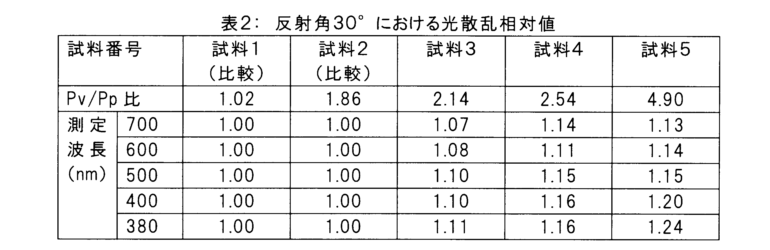
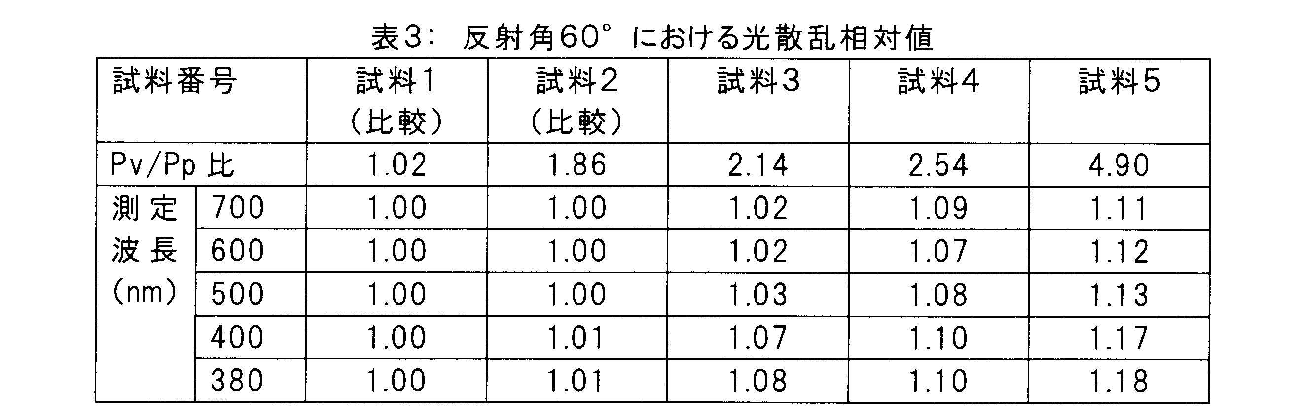
その結果、各測定反射角及び、各測定波長領域において、Pv/Ppが2.0以上の時、0.1以上の散乱効果がえられた。
例2:各種表面性状の電極箔の作製及び評価
例1の試料2~5に示される各種の条件を適宜変更して、図8に示される算術平均粗さRa及びPv/Pp比を有する各種の電極箔を作製した。これらの電極箔について例1と同様にして光散乱特性を評価したところ、図8に示されるように、Pv/Pp比が2.0以上の試料はいずれも光散乱特性が1.2倍向上する一方、Pv/Pp比が2.0未満の試料はそのような高い光散乱性が得られなかった。また、これらの電極箔を用いて発光素子又は発電素子を作製したところ、図8に示されるように、Raが60nm以下の場合には対向電極との短絡を回避して初期の素子特性が得られた。したがって、Pv/Pp比が2.0以上で、かつ、Raが60nm以下の表面プロファイルが好ましいことが分かる。
例1の試料2~5に示される各種の条件を適宜変更して、図8に示される算術平均粗さRa及びPv/Pp比を有する各種の電極箔を作製した。これらの電極箔について例1と同様にして光散乱特性を評価したところ、図8に示されるように、Pv/Pp比が2.0以上の試料はいずれも光散乱特性が1.2倍向上する一方、Pv/Pp比が2.0未満の試料はそのような高い光散乱性が得られなかった。また、これらの電極箔を用いて発光素子又は発電素子を作製したところ、図8に示されるように、Raが60nm以下の場合には対向電極との短絡を回避して初期の素子特性が得られた。したがって、Pv/Pp比が2.0以上で、かつ、Raが60nm以下の表面プロファイルが好ましいことが分かる。
図8に矢印で特定される試料6の光散乱面をSEM(1000倍)で観察したところ、図9に示されるように凹凸形状の判別が困難であった。そこで、図8に矢印で特定される試料6及び7について表面プロファイルを非接触表面形状測定機(NewView5032、Zygo社製)で測定したところ、図10~図13に示されるプロファイル画像が得られた。図10及び11に示される表面プロファイルは本発明による光散乱効果の改善がみられた試料6に関するものであり、凸部の形成が抑制され凹部が優先的に形成された望ましい表面プロファイルである。一方、図12及び13に示される表面プロファイルは光散乱効果の改善に乏しかった試料7に関するものである。
例3:光電特性の評価
(1)光電素子の作製
図14に示されるように、電極箔として例2で得られた、銅箔82上にアルミニウム反射層83を備えた試料6及び7を用いて光電素子を作製した。まず、このアルミニウム反射層83に、スパッタリングによってZnOからなる厚さ20nmのn型半導体バッファ層84を形成した。このバッファ層84上に、プラズマCVD装置(サムコ社製、PD-2202L)を用いて、窒化ケイ素からなる層間絶縁膜を形成した。その際、厚さ0.1mm、幅2mm、長さ10mmの複数枚の薄ガラスを2mm幅で電極箔上に並べることにより、受光部となるべき個所を覆った。窒化ケイ素成膜後、薄ガラスを除去した。その後、電極箔80を、40~50℃に加熱したイソプロピルアルコール溶液で洗浄し、窒素ガスを用いて乾燥させた。次に、クロロベンゼン溶液中にP3HT(ポリ-3-ヘキシルチオフェン)とPCBM((6,6)-フェニル-C61-ブチル酸メチルエステル)を各々10mg/ml浸漬させ、24時間で25℃前後の環境下で放置させ、完全に溶解させた。P3HTとPCBMが溶解した混合クロロベンゼン溶液を1500rpmで電極箔80にスピンコートし、P3HT:PCBM層86aが100nmの厚さになるように調整した。次に、PEDOT:PSS(ポリ(3,4-エチレンジオキシチオフェン/ポリ(4-スチレンスルホネート))分散溶液(1.3重量%)を5000rpmで電極箔にスピンコートした。コーティングを180℃で30分間、ホットプレート上で乾燥させて、PEDOT:PSS層86bを得た。金を真空蒸着装置にて約100nmの厚さになるように成膜して対向電極88aを得た。その際、受光部となるべき箇所は、櫛形のメタルマスクを用いて光を遮蔽しないようにした。その後、150℃で30分間、不活性雰囲気(窒素)下で焼成を行った。こうして図14に示される光電素子を得た。
(1)光電素子の作製
図14に示されるように、電極箔として例2で得られた、銅箔82上にアルミニウム反射層83を備えた試料6及び7を用いて光電素子を作製した。まず、このアルミニウム反射層83に、スパッタリングによってZnOからなる厚さ20nmのn型半導体バッファ層84を形成した。このバッファ層84上に、プラズマCVD装置(サムコ社製、PD-2202L)を用いて、窒化ケイ素からなる層間絶縁膜を形成した。その際、厚さ0.1mm、幅2mm、長さ10mmの複数枚の薄ガラスを2mm幅で電極箔上に並べることにより、受光部となるべき個所を覆った。窒化ケイ素成膜後、薄ガラスを除去した。その後、電極箔80を、40~50℃に加熱したイソプロピルアルコール溶液で洗浄し、窒素ガスを用いて乾燥させた。次に、クロロベンゼン溶液中にP3HT(ポリ-3-ヘキシルチオフェン)とPCBM((6,6)-フェニル-C61-ブチル酸メチルエステル)を各々10mg/ml浸漬させ、24時間で25℃前後の環境下で放置させ、完全に溶解させた。P3HTとPCBMが溶解した混合クロロベンゼン溶液を1500rpmで電極箔80にスピンコートし、P3HT:PCBM層86aが100nmの厚さになるように調整した。次に、PEDOT:PSS(ポリ(3,4-エチレンジオキシチオフェン/ポリ(4-スチレンスルホネート))分散溶液(1.3重量%)を5000rpmで電極箔にスピンコートした。コーティングを180℃で30分間、ホットプレート上で乾燥させて、PEDOT:PSS層86bを得た。金を真空蒸着装置にて約100nmの厚さになるように成膜して対向電極88aを得た。その際、受光部となるべき箇所は、櫛形のメタルマスクを用いて光を遮蔽しないようにした。その後、150℃で30分間、不活性雰囲気(窒素)下で焼成を行った。こうして図14に示される光電素子を得た。
(2)光電特性の評価
得られた光電素子について、シミュレータ(三永電機製、XES-40S1)、IV測定器(ADCMT製、6241A)及びソフトウェア(サンライズ社製)を用いて太陽電池発電効率を、AM(エアマス):1.5(規準光)以下及び入射光強度:100mW/cm2の計測条件で測定した。測定結果は以下の表4及び図15に示されるとおりであった。
得られた光電素子について、シミュレータ(三永電機製、XES-40S1)、IV測定器(ADCMT製、6241A)及びソフトウェア(サンライズ社製)を用いて太陽電池発電効率を、AM(エアマス):1.5(規準光)以下及び入射光強度:100mW/cm2の計測条件で測定した。測定結果は以下の表4及び図15に示されるとおりであった。

表4及び図15に示されるように、Pv/Pp比が高い試料6においては、Pv/Pp比が低い試料7と比べて、曲線因子FF及び変換効率ηが有意に高いことから、発電効率が格段に優れていることが分かる。
例4:凹部のみ電極箔の作製及び評価
金属箔として厚さ35μmの市販の電解銅箔(三井金属鉱業社製、3EC-III)を用い、CMP処理を2分間行ったこと以外は、試料2と同様にして電極箔の作製を行い、試料8とした。この試料8の光散乱面をSEM(1000倍)で観察したところ、図16に示されるように実質的に凹部のみを有する表面性状が観察された。また、試料8について表面プロファイルを非接触表面形状測定機(NewView5032、Zygo社製)で測定したところ、図17及び18に示されるプロファイル画像が得られた。これらの結果から明らかなように、試料8の光散乱面は凸部が実質的に除去され、実質的に凹部のみが形成された極めて望ましい表面プロファイルを有していた。観察した凹部の殆どが深さ1μm以下、長手方向長さ100μm以下のものであった。凹部の個数を、SEM1000倍視野(10000μm2)の視野においてカウントしたところ約170個であった。このような実質的に凹部のみが形成された電極箔にあっては、電極間の短絡をより一層確実に防止しながら、より優れた光散乱性を発揮することができ、それにより発光効率や発電効率が更に向上することが可能である。
金属箔として厚さ35μmの市販の電解銅箔(三井金属鉱業社製、3EC-III)を用い、CMP処理を2分間行ったこと以外は、試料2と同様にして電極箔の作製を行い、試料8とした。この試料8の光散乱面をSEM(1000倍)で観察したところ、図16に示されるように実質的に凹部のみを有する表面性状が観察された。また、試料8について表面プロファイルを非接触表面形状測定機(NewView5032、Zygo社製)で測定したところ、図17及び18に示されるプロファイル画像が得られた。これらの結果から明らかなように、試料8の光散乱面は凸部が実質的に除去され、実質的に凹部のみが形成された極めて望ましい表面プロファイルを有していた。観察した凹部の殆どが深さ1μm以下、長手方向長さ100μm以下のものであった。凹部の個数を、SEM1000倍視野(10000μm2)の視野においてカウントしたところ約170個であった。このような実質的に凹部のみが形成された電極箔にあっては、電極間の短絡をより一層確実に防止しながら、より優れた光散乱性を発揮することができ、それにより発光効率や発電効率が更に向上することが可能である。
Claims (19)
- 厚さ1~250μmの金属箔を備えてなる電極箔であって、
前記電極箔の少なくとも一方の最表面に、JIS B 0601-2001に準拠して181μm×136μmの矩形領域に対して測定される、断面曲線の最大山高さPpに対する断面曲線の最大谷深さPvのPv/Pp比が2.0以上である光散乱面を備えてなる、電極箔。 - 前記Pv/Pp比が2.5以上である、請求項1に記載の電極箔。
- 前記光散乱面が、JIS B 0601-2001に準拠して測定される、60nm以下の算術平均粗さRaを有する、請求項1又は2に記載の電極箔。
- 10~150μmの厚さを有する、請求項1~3のいずれか一項に記載の電極箔。
- 1~50μmの厚さを有する、請求項1~3のいずれか一項に記載の電極箔。
- 前記金属箔が、銅箔である、請求項1~5のいずれか一項に記載の電極箔。
- 前記金属箔の少なくとも一方の面に設けられる反射層をさらに備えてなり、前記反射層の表面が前記光散乱面を構成する、請求項1~6のいずれか一項に記載の電極箔。
- 前記金属箔の少なくとも一方の面に直接設けられる透明又は半透明のバッファ層をさらに備えてなり、前記バッファ層の表面が前記光散乱面を構成する、請求項1~6のいずれか一項に記載の電極箔。
- 前記金属箔の少なくとも一方の面に設けられる反射層と、該反射層上に直接設けられる透明又は半透明のバッファ層とをさらに備えてなり、前記バッファ層の表面が前記光散乱面を構成する、請求項1~6のいずれか一項に記載の電極箔。
- 前記電極箔が、1~300μmの厚さを有する、請求項1~9のいずれか一項に記載の電極箔。
- フレキシブル電子デバイスの支持基材を兼ねた電極として用いられる、請求項1~10のいずれか一項に記載の電極箔。
- 発光素子又は光電素子の電極として用いられる、請求項1~11のいずれか一項に記載の電極箔。
- 前記光散乱面を前記電極箔の両面に備えた、請求項1~12のいずれか一項に記載の電極箔。
- 前記光散乱面が、深さ1μm以下で長軸径100μm以下の凹部を無数に有し、該凹部が10000μm2の領域内に200個以下存在する、請求項1~13のいずれか一項に記載の電極箔。
- 請求項1~14のいずれか一項に記載の電極箔と、
前記電極箔の前記光散乱面上に設けられる、半導体特性を有する半導体機能層と、
を備えた、電子デバイス。 - 前記半導体機能層が前記光散乱面に直接形成されてなる、請求項15に記載の電子デバイス。
- 前記半導体機能層が励起発光又は光励起発電の機能を有し、それにより前記電子デバイスが発光素子又は光電素子として機能する、請求項15又は16に記載の電子デバイス。
- 前記半導体機能層上に透明又は半透明の対向電極を備えた、請求項15~17のいずれか一項に記載の電子デバイス。
- 前記半導体機能層を前記電極箔の両面に備えた、請求項15~18のいずれか一項に記載の電子デバイス。
Priority Applications (2)
| Application Number | Priority Date | Filing Date | Title |
|---|---|---|---|
| US13/981,804 US9029885B2 (en) | 2012-04-23 | 2012-12-26 | Electrode foil and electronic device |
| EP12875694.7A EP2844038B1 (en) | 2012-04-23 | 2012-12-26 | Electrode foil and electronic device |
Applications Claiming Priority (2)
| Application Number | Priority Date | Filing Date | Title |
|---|---|---|---|
| JP2012-097854 | 2012-04-23 | ||
| JP2012097854A JP5297546B1 (ja) | 2012-04-23 | 2012-04-23 | 電極箔及び電子デバイス |
Publications (1)
| Publication Number | Publication Date |
|---|---|
| WO2013161129A1 true WO2013161129A1 (ja) | 2013-10-31 |
Family
ID=49396810
Family Applications (1)
| Application Number | Title | Priority Date | Filing Date |
|---|---|---|---|
| PCT/JP2012/083620 Ceased WO2013161129A1 (ja) | 2012-04-23 | 2012-12-26 | 電極箔及び電子デバイス |
Country Status (5)
| Country | Link |
|---|---|
| US (1) | US9029885B2 (ja) |
| EP (1) | EP2844038B1 (ja) |
| JP (1) | JP5297546B1 (ja) |
| TW (1) | TWI508345B (ja) |
| WO (1) | WO2013161129A1 (ja) |
Cited By (1)
| Publication number | Priority date | Publication date | Assignee | Title |
|---|---|---|---|---|
| WO2020208774A1 (ja) * | 2019-04-11 | 2020-10-15 | シャープ株式会社 | 発光素子および表示装置 |
Families Citing this family (16)
| Publication number | Priority date | Publication date | Assignee | Title |
|---|---|---|---|---|
| KR101597749B1 (ko) * | 2012-07-27 | 2016-02-25 | 미쓰이금속광업주식회사 | 금속박 및 전자 디바이스 |
| JP6039540B2 (ja) * | 2013-12-13 | 2016-12-07 | 三井金属鉱業株式会社 | 電解銅箔及びその製造方法 |
| JP6431486B2 (ja) * | 2013-12-26 | 2018-11-28 | 株式会社カネカ | 太陽電池のi‐v測定方法、太陽電池のi‐v測定装置、太陽電池の製造方法、太陽電池モジュールの製造方法、および太陽電池モジュール |
| DE102014106549B4 (de) * | 2014-05-09 | 2023-10-19 | Pictiva Displays International Limited | Organisches Licht emittierendes Bauelement |
| WO2016134703A1 (de) * | 2015-02-26 | 2016-09-01 | Dynamic Solar Systems Ag | Raumtemperatur-verfahren zur herstellung elektrotechnischer dünnschichten und verfahrensgemäss erhaltene dünnschichtfolge |
| MY186397A (en) * | 2015-07-29 | 2021-07-22 | Namics Corp | Roughened copper foil, copper-clad laminate, and printed wiring board |
| US20190013155A1 (en) * | 2016-02-19 | 2019-01-10 | Sekisui Chemical Co., Ltd. | Solid junction-type photovoltaic device and method for producing same |
| JP6745116B2 (ja) * | 2016-02-23 | 2020-08-26 | 積水化学工業株式会社 | フレキシブル太陽電池 |
| GB2554422A (en) * | 2016-09-27 | 2018-04-04 | Sumitomo Chemical Co | Organic microcavity photodetectors with narrow and tunable spectral response |
| JP2019536210A (ja) * | 2016-11-09 | 2019-12-12 | ケンブリッジ エンタープライズ リミティッド | リチウムイオン電池用アノード材料 |
| DE102017123154B4 (de) * | 2017-10-05 | 2025-07-03 | OSRAM Opto Semiconductors Gesellschaft mit beschränkter Haftung | Verfahren zur Herstellung eines optoelektronischen Bauelements und optoelektronisches Bauelement |
| JP7308831B2 (ja) * | 2017-12-14 | 2023-07-14 | ルミレッズ リミテッド ライアビリティ カンパニー | Ledダイの汚染を防止する方法 |
| TWI760906B (zh) * | 2020-10-28 | 2022-04-11 | 肇昇精密科技有限公司 | 預浸料製造設備及其加熱件 |
| CN114449693A (zh) * | 2020-10-30 | 2022-05-06 | 肇昇精密科技有限公司 | 预浸料制造设备及其加热件 |
| US20260059939A1 (en) * | 2022-08-22 | 2026-02-26 | Sharp Display Technology Corporation | Light-emitting element, display device, and method for manufacturing the light-emiting element |
| WO2024150719A1 (ja) * | 2023-01-10 | 2024-07-18 | 東洋紡株式会社 | 光電変換素子の製造方法および光電変換素子 |
Citations (8)
| Publication number | Priority date | Publication date | Assignee | Title |
|---|---|---|---|---|
| JP2005216705A (ja) * | 2004-01-30 | 2005-08-11 | Toppan Printing Co Ltd | 有機el表示素子およびその製造方法 |
| JP2007234254A (ja) * | 2006-02-27 | 2007-09-13 | Sanyo Electric Co Ltd | 有機エレクトロルミネッセンス素子及びその製造方法 |
| JP2008243772A (ja) | 2007-03-29 | 2008-10-09 | Seiko Epson Corp | 発光装置およびその製造方法 |
| JP2009152113A (ja) | 2007-12-21 | 2009-07-09 | Rohm Co Ltd | 有機el素子 |
| WO2011111629A1 (ja) * | 2010-03-08 | 2011-09-15 | 旭硝子株式会社 | 有機led発光素子及びその製造方法 |
| JP2011222819A (ja) | 2010-04-12 | 2011-11-04 | Mitsubishi Chemicals Corp | 太陽電池 |
| WO2011152092A1 (ja) | 2010-06-04 | 2011-12-08 | 三井金属鉱業株式会社 | 電極箔および有機デバイス |
| WO2011152091A1 (ja) | 2010-06-04 | 2011-12-08 | 三井金属鉱業株式会社 | 電極箔および有機デバイス |
Family Cites Families (5)
| Publication number | Priority date | Publication date | Assignee | Title |
|---|---|---|---|---|
| SE514309C2 (sv) * | 1999-05-28 | 2001-02-05 | Ericsson Telefon Ab L M | Förfarande för att bestämma ytstruktur |
| KR100975491B1 (ko) * | 2005-03-31 | 2010-08-11 | 미쓰이 긴조꾸 고교 가부시키가이샤 | 전해 동박 및 전해 동박의 제조 방법 |
| JP2006331694A (ja) * | 2005-05-23 | 2006-12-07 | Matsushita Electric Works Ltd | 有機発光素子及び有機発光素子用基板 |
| JP5016712B2 (ja) * | 2010-09-21 | 2012-09-05 | 三井金属鉱業株式会社 | 電極箔および有機デバイス |
| JP5626644B2 (ja) * | 2010-11-18 | 2014-11-19 | 三洋電機株式会社 | リチウム二次電池負極用バインダー、リチウム二次電池用負極、リチウム二次電池、リチウム二次電池負極用バインダー前駆体溶液及びリチウム二次電池用負極の製造方法 |
-
2012
- 2012-04-23 JP JP2012097854A patent/JP5297546B1/ja active Active
- 2012-12-26 EP EP12875694.7A patent/EP2844038B1/en active Active
- 2012-12-26 US US13/981,804 patent/US9029885B2/en not_active Expired - Fee Related
- 2012-12-26 WO PCT/JP2012/083620 patent/WO2013161129A1/ja not_active Ceased
-
2013
- 2013-01-03 TW TW102100105A patent/TWI508345B/zh not_active IP Right Cessation
Patent Citations (8)
| Publication number | Priority date | Publication date | Assignee | Title |
|---|---|---|---|---|
| JP2005216705A (ja) * | 2004-01-30 | 2005-08-11 | Toppan Printing Co Ltd | 有機el表示素子およびその製造方法 |
| JP2007234254A (ja) * | 2006-02-27 | 2007-09-13 | Sanyo Electric Co Ltd | 有機エレクトロルミネッセンス素子及びその製造方法 |
| JP2008243772A (ja) | 2007-03-29 | 2008-10-09 | Seiko Epson Corp | 発光装置およびその製造方法 |
| JP2009152113A (ja) | 2007-12-21 | 2009-07-09 | Rohm Co Ltd | 有機el素子 |
| WO2011111629A1 (ja) * | 2010-03-08 | 2011-09-15 | 旭硝子株式会社 | 有機led発光素子及びその製造方法 |
| JP2011222819A (ja) | 2010-04-12 | 2011-11-04 | Mitsubishi Chemicals Corp | 太陽電池 |
| WO2011152092A1 (ja) | 2010-06-04 | 2011-12-08 | 三井金属鉱業株式会社 | 電極箔および有機デバイス |
| WO2011152091A1 (ja) | 2010-06-04 | 2011-12-08 | 三井金属鉱業株式会社 | 電極箔および有機デバイス |
Non-Patent Citations (1)
| Title |
|---|
| See also references of EP2844038A4 |
Cited By (1)
| Publication number | Priority date | Publication date | Assignee | Title |
|---|---|---|---|---|
| WO2020208774A1 (ja) * | 2019-04-11 | 2020-10-15 | シャープ株式会社 | 発光素子および表示装置 |
Also Published As
| Publication number | Publication date |
|---|---|
| EP2844038A1 (en) | 2015-03-04 |
| US20140061701A1 (en) | 2014-03-06 |
| TWI508345B (zh) | 2015-11-11 |
| EP2844038A4 (en) | 2016-01-13 |
| EP2844038B1 (en) | 2019-05-08 |
| JP2013225447A (ja) | 2013-10-31 |
| US9029885B2 (en) | 2015-05-12 |
| JP5297546B1 (ja) | 2013-09-25 |
| TW201347256A (zh) | 2013-11-16 |
Similar Documents
| Publication | Publication Date | Title |
|---|---|---|
| JP5297546B1 (ja) | 電極箔及び電子デバイス | |
| JP6141641B2 (ja) | 電解銅箔及び電子デバイス | |
| JP5016712B2 (ja) | 電極箔および有機デバイス | |
| JP5832034B2 (ja) | 電極箔および有機デバイス | |
| WO2013118325A1 (ja) | 電極箔および電子デバイス | |
| WO2011152092A1 (ja) | 電極箔および有機デバイス | |
| JP6039540B2 (ja) | 電解銅箔及びその製造方法 | |
| WO2012137525A1 (ja) | 有機デバイス用電極シート、有機デバイスモジュールおよびその製造方法 | |
| JP6134317B2 (ja) | 金属箔及び電子デバイス |
Legal Events
| Date | Code | Title | Description |
|---|---|---|---|
| WWE | Wipo information: entry into national phase |
Ref document number: 13981804 Country of ref document: US |
|
| 121 | Ep: the epo has been informed by wipo that ep was designated in this application |
Ref document number: 12875694 Country of ref document: EP Kind code of ref document: A1 |
|
| WWE | Wipo information: entry into national phase |
Ref document number: 2012875694 Country of ref document: EP |
|
| NENP | Non-entry into the national phase |
Ref country code: DE |