WO2013161129A1 - Feuille d'électrode et dispositif électronique - Google Patents
Feuille d'électrode et dispositif électronique Download PDFInfo
- Publication number
- WO2013161129A1 WO2013161129A1 PCT/JP2012/083620 JP2012083620W WO2013161129A1 WO 2013161129 A1 WO2013161129 A1 WO 2013161129A1 JP 2012083620 W JP2012083620 W JP 2012083620W WO 2013161129 A1 WO2013161129 A1 WO 2013161129A1
- Authority
- WO
- WIPO (PCT)
- Prior art keywords
- electrode foil
- electrode
- layer
- foil
- light scattering
- Prior art date
- Legal status (The legal status is an assumption and is not a legal conclusion. Google has not performed a legal analysis and makes no representation as to the accuracy of the status listed.)
- Ceased
Links
Images






Classifications
-
- H—ELECTRICITY
- H05—ELECTRIC TECHNIQUES NOT OTHERWISE PROVIDED FOR
- H05B—ELECTRIC HEATING; ELECTRIC LIGHT SOURCES NOT OTHERWISE PROVIDED FOR; CIRCUIT ARRANGEMENTS FOR ELECTRIC LIGHT SOURCES, IN GENERAL
- H05B33/00—Electroluminescent light sources
- H05B33/12—Light sources with substantially two-dimensional [2D] radiating surfaces
- H05B33/26—Light sources with substantially two-dimensional [2D] radiating surfaces characterised by the composition or arrangement of the conductive material used as an electrode
-
- H—ELECTRICITY
- H10—SEMICONDUCTOR DEVICES; ELECTRIC SOLID-STATE DEVICES NOT OTHERWISE PROVIDED FOR
- H10F—INORGANIC SEMICONDUCTOR DEVICES SENSITIVE TO INFRARED RADIATION, LIGHT, ELECTROMAGNETIC RADIATION OF SHORTER WAVELENGTH OR CORPUSCULAR RADIATION
- H10F77/00—Constructional details of devices covered by this subclass
- H10F77/10—Semiconductor bodies
- H10F77/16—Material structures, e.g. crystalline structures, film structures or crystal plane orientations
- H10F77/169—Thin semiconductor films on metallic or insulating substrates
-
- H—ELECTRICITY
- H10—SEMICONDUCTOR DEVICES; ELECTRIC SOLID-STATE DEVICES NOT OTHERWISE PROVIDED FOR
- H10F—INORGANIC SEMICONDUCTOR DEVICES SENSITIVE TO INFRARED RADIATION, LIGHT, ELECTROMAGNETIC RADIATION OF SHORTER WAVELENGTH OR CORPUSCULAR RADIATION
- H10F77/00—Constructional details of devices covered by this subclass
- H10F77/40—Optical elements or arrangements
- H10F77/42—Optical elements or arrangements directly associated or integrated with photovoltaic cells, e.g. light-reflecting means or light-concentrating means
- H10F77/48—Back surface reflectors [BSR]
-
- H—ELECTRICITY
- H10—SEMICONDUCTOR DEVICES; ELECTRIC SOLID-STATE DEVICES NOT OTHERWISE PROVIDED FOR
- H10H—INORGANIC LIGHT-EMITTING SEMICONDUCTOR DEVICES HAVING POTENTIAL BARRIERS
- H10H20/00—Individual inorganic light-emitting semiconductor devices having potential barriers, e.g. light-emitting diodes [LED]
- H10H20/80—Constructional details
- H10H20/83—Electrodes
- H10H20/831—Electrodes characterised by their shape
-
- H—ELECTRICITY
- H10—SEMICONDUCTOR DEVICES; ELECTRIC SOLID-STATE DEVICES NOT OTHERWISE PROVIDED FOR
- H10K—ORGANIC ELECTRIC SOLID-STATE DEVICES
- H10K50/00—Organic light-emitting devices
- H10K50/80—Constructional details
- H10K50/85—Arrangements for extracting light from the devices
- H10K50/854—Arrangements for extracting light from the devices comprising scattering means
-
- H—ELECTRICITY
- H10—SEMICONDUCTOR DEVICES; ELECTRIC SOLID-STATE DEVICES NOT OTHERWISE PROVIDED FOR
- H10K—ORGANIC ELECTRIC SOLID-STATE DEVICES
- H10K77/00—Constructional details of devices covered by this subclass and not covered by groups H10K10/80, H10K30/80, H10K50/80 or H10K59/80
- H10K77/10—Substrates, e.g. flexible substrates
-
- H—ELECTRICITY
- H10—SEMICONDUCTOR DEVICES; ELECTRIC SOLID-STATE DEVICES NOT OTHERWISE PROVIDED FOR
- H10H—INORGANIC LIGHT-EMITTING SEMICONDUCTOR DEVICES HAVING POTENTIAL BARRIERS
- H10H20/00—Individual inorganic light-emitting semiconductor devices having potential barriers, e.g. light-emitting diodes [LED]
- H10H20/80—Constructional details
- H10H20/83—Electrodes
- H10H20/832—Electrodes characterised by their material
- H10H20/833—Transparent materials
-
- H—ELECTRICITY
- H10—SEMICONDUCTOR DEVICES; ELECTRIC SOLID-STATE DEVICES NOT OTHERWISE PROVIDED FOR
- H10H—INORGANIC LIGHT-EMITTING SEMICONDUCTOR DEVICES HAVING POTENTIAL BARRIERS
- H10H20/00—Individual inorganic light-emitting semiconductor devices having potential barriers, e.g. light-emitting diodes [LED]
- H10H20/80—Constructional details
- H10H20/83—Electrodes
- H10H20/832—Electrodes characterised by their material
- H10H20/835—Reflective materials
-
- H—ELECTRICITY
- H10—SEMICONDUCTOR DEVICES; ELECTRIC SOLID-STATE DEVICES NOT OTHERWISE PROVIDED FOR
- H10K—ORGANIC ELECTRIC SOLID-STATE DEVICES
- H10K30/00—Organic devices sensitive to infrared radiation, light, electromagnetic radiation of shorter wavelength or corpuscular radiation
- H10K30/80—Constructional details
- H10K30/87—Light-trapping means
-
- Y—GENERAL TAGGING OF NEW TECHNOLOGICAL DEVELOPMENTS; GENERAL TAGGING OF CROSS-SECTIONAL TECHNOLOGIES SPANNING OVER SEVERAL SECTIONS OF THE IPC; TECHNICAL SUBJECTS COVERED BY FORMER USPC CROSS-REFERENCE ART COLLECTIONS [XRACs] AND DIGESTS
- Y02—TECHNOLOGIES OR APPLICATIONS FOR MITIGATION OR ADAPTATION AGAINST CLIMATE CHANGE
- Y02E—REDUCTION OF GREENHOUSE GAS [GHG] EMISSIONS, RELATED TO ENERGY GENERATION, TRANSMISSION OR DISTRIBUTION
- Y02E10/00—Energy generation through renewable energy sources
- Y02E10/50—Photovoltaic [PV] energy
- Y02E10/52—PV systems with concentrators
-
- Y—GENERAL TAGGING OF NEW TECHNOLOGICAL DEVELOPMENTS; GENERAL TAGGING OF CROSS-SECTIONAL TECHNOLOGIES SPANNING OVER SEVERAL SECTIONS OF THE IPC; TECHNICAL SUBJECTS COVERED BY FORMER USPC CROSS-REFERENCE ART COLLECTIONS [XRACs] AND DIGESTS
- Y02—TECHNOLOGIES OR APPLICATIONS FOR MITIGATION OR ADAPTATION AGAINST CLIMATE CHANGE
- Y02E—REDUCTION OF GREENHOUSE GAS [GHG] EMISSIONS, RELATED TO ENERGY GENERATION, TRANSMISSION OR DISTRIBUTION
- Y02E10/00—Energy generation through renewable energy sources
- Y02E10/50—Photovoltaic [PV] energy
- Y02E10/549—Organic PV cells
-
- Y—GENERAL TAGGING OF NEW TECHNOLOGICAL DEVELOPMENTS; GENERAL TAGGING OF CROSS-SECTIONAL TECHNOLOGIES SPANNING OVER SEVERAL SECTIONS OF THE IPC; TECHNICAL SUBJECTS COVERED BY FORMER USPC CROSS-REFERENCE ART COLLECTIONS [XRACs] AND DIGESTS
- Y10—TECHNICAL SUBJECTS COVERED BY FORMER USPC
- Y10T—TECHNICAL SUBJECTS COVERED BY FORMER US CLASSIFICATION
- Y10T428/00—Stock material or miscellaneous articles
- Y10T428/12—All metal or with adjacent metals
- Y10T428/12993—Surface feature [e.g., rough, mirror]
-
- Y—GENERAL TAGGING OF NEW TECHNOLOGICAL DEVELOPMENTS; GENERAL TAGGING OF CROSS-SECTIONAL TECHNOLOGIES SPANNING OVER SEVERAL SECTIONS OF THE IPC; TECHNICAL SUBJECTS COVERED BY FORMER USPC CROSS-REFERENCE ART COLLECTIONS [XRACs] AND DIGESTS
- Y10—TECHNICAL SUBJECTS COVERED BY FORMER USPC
- Y10T—TECHNICAL SUBJECTS COVERED BY FORMER US CLASSIFICATION
- Y10T428/00—Stock material or miscellaneous articles
- Y10T428/24—Structurally defined web or sheet [e.g., overall dimension, etc.]
- Y10T428/24355—Continuous and nonuniform or irregular surface on layer or component [e.g., roofing, etc.]
-
- Y—GENERAL TAGGING OF NEW TECHNOLOGICAL DEVELOPMENTS; GENERAL TAGGING OF CROSS-SECTIONAL TECHNOLOGIES SPANNING OVER SEVERAL SECTIONS OF THE IPC; TECHNICAL SUBJECTS COVERED BY FORMER USPC CROSS-REFERENCE ART COLLECTIONS [XRACs] AND DIGESTS
- Y10—TECHNICAL SUBJECTS COVERED BY FORMER USPC
- Y10T—TECHNICAL SUBJECTS COVERED BY FORMER US CLASSIFICATION
- Y10T428/00—Stock material or miscellaneous articles
- Y10T428/24—Structurally defined web or sheet [e.g., overall dimension, etc.]
- Y10T428/24355—Continuous and nonuniform or irregular surface on layer or component [e.g., roofing, etc.]
- Y10T428/24364—Continuous and nonuniform or irregular surface on layer or component [e.g., roofing, etc.] with transparent or protective coating
Definitions
- the present invention relates to an electrode foil using a metal foil and an electronic device such as a light emitting element and a photoelectric element using the same.
- organic EL lighting In recent years, light-emitting elements such as organic EL lighting have attracted attention as environmentally friendly green devices.
- Features of organic EL lighting include 1) low power consumption compared to incandescent lamps, 2) thin and lightweight, and 3) flexibility.
- organic EL lighting is being developed to realize the features 2) and 3). In this regard, it is impossible to realize the characteristics 2) and 3) above with a glass substrate that has been conventionally used in flat panel displays (FPD) or the like.
- Ultra-thin glass is excellent in heat resistance, barrier properties, and light transmission properties, and has good flexibility, but handling properties are slightly inferior, thermal conductivity is low, and material cost is high.
- the resin film is excellent in handling properties and flexibility, has a low material cost, and has good light transmittance, but has poor heat resistance and barrier properties, and has low thermal conductivity.
- the metal foil has excellent characteristics such as excellent heat resistance, barrier properties, handling properties, thermal conductivity, good flexibility, and low material cost, except that it has no light transmittance.
- the thermal conductivity of a typical flexible glass or film is as low as 1 W / m ° C. or less, whereas in the case of a copper foil, it is as high as about 280 W / m ° C.
- Patent Document 1 Japanese Patent Laid-Open No. 2009-152113
- Patent Document 2 Japanese Patent Laid-Open No. 2008-243772 proposes that a nickel plating layer is provided on a metal substrate so that a smooth surface is formed without polishing and an organic EL element is formed thereon.
- Patent Document 3 Japanese Patent Application Laid-Open No.
- Patent Document 4 International Application No. 2011/152091
- Patent Document 5 International Application No. 2011/152092
- the arithmetic average roughness Ra is extremely low as 10.0 nm or less. It has been proposed to use a metal foil having a surface as a supporting substrate and electrode.
- a microlens or the like is disposed on the surface of the substrate on the light extraction side. Attempts have been made to improve luminous efficiency.
- formation of a microlens or the like is not advantageous from the viewpoint of productivity and cost because fine processing is required, and therefore, it is difficult to say that it is suitable for increasing the area.
- Inventors of the present invention by imparting a specific surface profile with a concave advantage to the surface of the metal foil itself, prevents short-circuiting between electrodes when used in electronic devices such as light-emitting elements and photoelectric elements.
- an electrode foil capable of exhibiting excellent light scattering properties was obtained, and it was found that the electrode foil itself can improve luminous efficiency and power generation efficiency.
- an object of the present invention is to provide an electrode foil capable of exhibiting excellent light scattering properties while preventing a short circuit between the electrodes.
- an electrode foil comprising a metal foil having a thickness of 1 to 250 ⁇ m, wherein at least one outermost surface of the electrode foil is 181 ⁇ m ⁇ 136 ⁇ m in accordance with JIS B 0601-2001.
- an electrode foil comprising a light scattering surface having a Pv / Pp ratio of 2.0 or more of the maximum valley depth Pv of the cross-sectional curve to the maximum peak height Pp of the cross-sectional curve measured with respect to the rectangular region of Is done.
- the electrode foil A semiconductor functional layer having semiconductor characteristics, provided on the light scattering surface of the electrode foil; An electronic device is provided.
- FIG. 1 It is a schematic cross section which shows an example of the electrode foil by this invention. It is a schematic cross section which shows an example of the organic EL element which used the electrode foil by this invention as an anode. It is a schematic cross section which shows an example of the top emission type organic EL illumination by this invention. It is a schematic cross section which shows an example of the organic EL element which used the electrode foil by this invention as a cathode. It is a figure explaining an example of the lamination
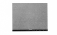
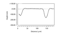
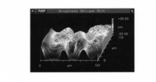
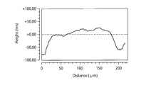
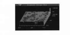
- FIG. 8 It is the image which observed the surface of the sample 6 shown by FIG. 8 by SEM (1000 times). It is the surface three-dimensional profile obtained by measuring the surface of the sample 6 shown by FIG. 8 with a non-contact surface shape measuring machine. It is the surface profile obtained by measuring the surface of the sample 6 shown by FIG. 8 with a non-contact surface shape measuring machine. It is the surface three-dimensional profile obtained by measuring the surface of the sample 7 shown by FIG. 8 with a non-contact surface shape measuring machine. It is the surface profile obtained by measuring the surface of the sample 7 shown by FIG. 8 with a non-contact surface shape measuring machine.
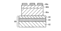
- FIG. 6 is a schematic cross-sectional view showing a layer configuration of a photoelectric element manufactured in Example 3.
- FIG. It is a figure which shows the relationship between the voltage measured with respect to the photoelectric element in Example 3, and an electric current. It is the image which observed the surface of the sample 8 produced in Example 4 by SEM (1000 times). It is the surface three-dimensional profile obtained by measuring the surface of the sample 8 shown by FIG. 16 with a non-contact surface shape measuring machine. It is the surface profile obtained by measuring the surface of the sample 8 shown by FIG. 16 with a non-contact surface shape measuring machine.
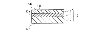
- FIG. 1 shows a schematic cross-sectional view of an example of an electrode foil according to the present invention.
- the electrode foil 10 shown in FIG. 1 has a metal foil 12 having a thickness of 1 to 250 ⁇ m.
- the electrode foil 10 may include a reflective layer 13 provided on one or both surfaces of the metal foil 12 directly or via a diffusion prevention layer as desired.
- the electrode foil 10 may include a buffer layer 14 provided directly on at least one surface or both surfaces of the metal foil 12 or the surface of the reflective layer 13 (if present) as desired.
- the electrode foil of the present invention is not limited to this, and has a one-layer configuration of the metal foil 12.
- the metal foil 12 There may be a two-layer structure of the metal foil 12 and the reflective layer 13. Alternatively, a five-layer configuration in which the reflective layer 13 and the buffer layer 14 are provided on both surfaces of the metal foil 12 may be employed.
- At least one outermost surface of the electrode foil 10 has a maximum valley depth Pv of the cross-sectional curve with respect to a maximum peak height Pp of the cross-sectional curve measured with respect to a rectangular area of 181 ⁇ m ⁇ 136 ⁇ m according to JIS B 0601-2001.
- a light scattering surface having a Pv / Pp ratio of 2.0 or more is provided.
- the maximum peak height Pp represents the height of the convex portion, while the maximum valley depth Pv represents the depth of the concave portion. Therefore, a Pv / Pp ratio of 2.0 or more means a specific surface profile having a concave portion preferentially over a convex portion.
- the electrode foil itself can exhibit excellent light scattering properties.
- the luminous efficiency and power generation efficiency can be improved with the electrode foil itself. This is because light is scattered due to the preferentially formed concave portions, and the formation of the convex portions is suppressed, thereby causing a short circuit between the electrodes (specifically, a short circuit with the counter electrode or between the semiconductor functional layers). This is thought to be due to prevention of short circuit.
- a preferable Pv / Pp ratio is 2.3 or more, more preferably 2.5 or more, still more preferably 2.8 or more, and particularly preferably 3.0 or more.
- the maximum peak height Pp and the maximum valley depth Pv can be measured in accordance with JIS B 0601-2001 using a commercially available non-contact surface shape measuring machine.
- the light scattering surface of the electrode foil 10 is the surface of the metal foil 12 in the case of a single layer configuration, and the outermost reflective layer 13 in the case of a multi-layer configuration including the reflective layer 13 and the buffer layer 14. Or the surface of the buffer layer 14 is meant.
- the above Pv / Pp ratio is realized by changing the Pv / Pp ratio of the surface 12a of the metal foil 12 on which the reflective layer 13 and / or the buffer layer 14 are formed as described above. Range, that is, 2.0 or more, preferably 2.3 or more, more preferably 2.5 or more, further preferably 2.8 or more, particularly preferably 3.0 or more, most preferably 3.3 or more.
- the reflective layer 13 and / or the buffer layer 14 can be formed thereon.
- a Pv / Pp ratio equal to or slightly higher than the arithmetic average roughness Pv / Pp ratio to be imparted on the outermost surface is imparted to the surface of the lower layer or foil.
- the evaluation of the Pv / Pp ratio of the surface of the metal foil that does not constitute the outermost surface due to the laminated state is made by creating a cross section from the surface of the metal foil by FIB (Focused Ion Beam) processing, The evaluation of the Pv / Pp ratio on the surface of the reflective layer that does not constitute the outermost surface due to the laminated state can be performed in the same manner.
- the light scattering surface of the electrode foil 10 preferably has innumerable recesses having a depth of 1 ⁇ m or less (typically 0.1 to 1 ⁇ m) and a major axis diameter of 100 ⁇ m or less (typically 1 to 100 ⁇ m).
- a depth typically 0.1 to 1 ⁇ m
- a major axis diameter typically 100 ⁇ m or less
- 200 or less (typically 1 to 200) of such recesses exist in a 10,000 ⁇ m 2 region.
- the metal foil 12 as an electrode as well as a supporting substrate, an electrode foil having the functions of a supporting substrate and an electrode can be provided.
- the thickness of the metal foil 12 is set to 1 to 250 ⁇ m, it can be used as an electrode that also serves as a supporting substrate for a flexible electronic device.
- the electrode foil 12 of the present invention is based on a metal foil, so that a support base material is not particularly required, for example, roll-to-roll. It can be manufactured efficiently by the process.
- the roll-to-roll process is an extremely advantageous process for efficiently mass-producing electronic devices in which a long foil wound in a roll shape is drawn out and subjected to a predetermined process and then wound up again.
- the electrode foil of this invention can make a support base material and a reflection layer unnecessary. For this reason, it is preferable that the electrode foil of this invention does not have an insulating layer in the part by which an electronic device is constructed
- the metal foil 12 is not particularly limited as long as it is a foil-like metal material having strength as a supporting substrate and electrical characteristics necessary as an electrode.
- a preferred metal foil is a nonmagnetic metal foil from the viewpoint of preventing adhesion of particulate matter generated during processing due to magnetism.
- Preferred examples of the nonmagnetic metal include copper, aluminum, nonmagnetic stainless steel, titanium, tantalum, and molybdenum, and more preferred are copper, aluminum, and nonmagnetic stainless steel.
- the most preferred metal foil is a copper foil. Copper foil is excellent in strength, flexibility, electrical characteristics and the like while being relatively inexpensive.
- the light scattering surface of the electrode foil 10 is preferably an ultra flat surface having an arithmetic average roughness Ra of 60.0 nm or less, more preferably 30.0 nm or less, still more preferably 20.0 nm or less, particularly preferably 10 It is 0.0 nm or less, more preferably 7.0 nm or less, and the roughness may be appropriately determined according to the application and performance required for the electrode foil.
- the lower limit of the arithmetic average roughness Ra is not particularly limited and may be zero. However, in consideration of the efficiency of the flattening process, 0.5 nm is cited as a guideline for the lower limit value.
- This arithmetic average roughness Ra can be measured using a commercially available roughness measuring device in accordance with JIS B 0601-2001.
- the light scattering surface of the electrode foil 10 is the surface of the metal foil 12 in the case of a single layer configuration, and is the outermost reflective layer in the case of a multi-layer configuration including the reflective layer 13 and the buffer layer 14. 13 or the surface of the buffer layer 14.
- realization of the said arithmetic mean roughness Ra in the case of such a multi-layer structure is the arithmetic mean roughness Ra of the surface 12a of the metal foil 12 in which the reflective layer 13 and / or the buffer layer 14 are formed.
- the reflection layer 13 and / or the buffer layer 14 can be formed thereon.
- an arithmetic average roughness Ra that is equal to or slightly smaller than the arithmetic average roughness Ra to be applied on the outermost surface is provided on the surface of the lower layer or foil.
- the arithmetic average roughness Ra of the surface of the metal foil that does not constitute the outermost surface due to the laminated state is evaluated by creating a cross section from the surface of the metal foil by FIB (Focused Ion Beam) processing, and using the transmission electron microscope (TEM), and the arithmetic average roughness Ra of the reflective layer surface that does not constitute the outermost surface due to the laminated state can be evaluated in the same manner.
- FIB Flucused Ion Beam
- Such an ultra-flat surface is formed by CMP (Chemical Mechanical This can be realized by polishing the metal foil by a polishing process.
- the CMP treatment can be performed according to known conditions using a known polishing liquid and a known polishing pad.
- a preferable polishing liquid it contains about 0.1 to 10% by weight of one or more kinds of abrasive grains selected from ceria, silica, alumina, zirconia and the like, and rust prevention such as benzotriazole (BTA).
- a preferable polishing pad includes a urethane pad.
- the polishing conditions are not particularly limited as long as the pad rotation speed, work load, polishing liquid application flow rate, etc. are adjusted appropriately, but the rotation speed is in the range of 20 to 1000 rpm, and the work load is in the range of 100 to 500 gf / cm 2 . In addition, it is preferable to adjust the polishing liquid application flow rate within the range of 20 to 200 cc / min.
- the ultra-flat surface 12a of the metal foil 12 can also be realized by polishing the metal foil 12 using an electrolytic polishing method, a buff polishing method, a chemical polishing method, or a combination thereof.
- the chemical polishing method is not particularly limited as long as the chemical solution, the chemical solution temperature, the chemical solution immersion time, etc. are appropriately adjusted.
- the chemical polishing of copper foil uses a mixture of 2-aminoethanol and ammonium chloride. Can be performed.
- the temperature of the chemical solution is preferably room temperature, and it is preferable to use an immersion method (Dip method). Further, since the chemical solution immersion time tends to deteriorate the flatness as it becomes longer, it is preferably 10 to 120 seconds, and more preferably 30 to 90 seconds.
- the metal foil after chemical polishing is preferably washed with running water. According to such a planarization process, it is possible to planarize a surface having a Ra arithmetic average roughness Ra of about 12 nm to Ra 10.0 nm or less, for example, about 3.0 nm.
- the ultra-flat surface 12a may be realized by a method of polishing the surface of the metal foil 12 by blasting, a method of rapidly cooling the surface of the metal foil 12 by melting it by a technique such as laser, resistance heating, or lamp heating. it can.
- the ultra-flat surface 12a obtained as described above cannot normally have a Pv / Pp ratio of 2.0 or more. Therefore, it is preferable to perform a process for imparting a Pv / Pp ratio of 2.0 or more to the ultra flat surface 12a.
- Preferable examples of such surface treatment include ultrasonic cleaning, chemical polishing using a chemical polishing liquid, and / or dry ice blasting.
- the ultrasonic cleaning can be performed, for example, by treating the surface of the metal foil for a predetermined time (for example, 10 minutes) with a predetermined high frequency output (for example, 60 W) using a commercially available flowing water type ultrasonic cleaning machine.
- a chemical polishing liquid for example, a polishing liquid for pure copper such as CPB-10 manufactured by Mitsubishi Gas Chemical Company
- the polishing liquid and water are mixed at a predetermined ratio (for example, a weight ratio of 1: 2). Then, it can be performed by immersing at room temperature for 1 minute, followed by washing with pure water, washing with dilute sulfuric acid (for example, 0.1N dilute sulfuric acid), washing with pure water again, and drying.
- a chemical polishing liquid for example, a polishing liquid for pure copper such as CPB-10 manufactured by Mitsubishi Gas Chemical Company
- dilute sulfuric acid for example, 0.1N dilute sulfuric acid
- the dry ice blasting method uses, for example, a commercially available apparatus such as a dry ice snow system (manufactured by Air Water) to inject carbon dioxide gas compressed to a high pressure from a thin nozzle, thereby causing the carbon dioxide solidified at a low temperature to be obtained on the ultra flat surface 12a. This can be done by spraying.
- a commercially available apparatus such as a dry ice snow system (manufactured by Air Water) to inject carbon dioxide gas compressed to a high pressure from a thin nozzle, thereby causing the carbon dioxide solidified at a low temperature to be obtained on the ultra flat surface 12a.
- This can be done by spraying.
- the electrolytic copper foil is electrodeposited, it is also possible to control the surface shape of the electrolytic copper foil by appropriately adjusting the presence or absence and amount of addition of organic matter, chlorine and the like.
- post-treatment for example, ultrasonic cleaning, chemical polishing, dry ice blast treatment, CMP treatment, etc.
- the thickness of the metal foil 12 is not particularly limited as long as it is a thickness that can be handled alone as a foil without impairing flexibility, but is 1 to 250 ⁇ m, preferably 5 to 200 ⁇ m, more preferably 10 to The thickness is 150 ⁇ m, more preferably 15 to 100 ⁇ m, but the thickness may be appropriately determined according to the application and performance required for the electrode foil. Therefore, the upper limit of the thickness is particularly preferably 50 ⁇ m, 35 ⁇ m, or 25 ⁇ m when reduction of the amount of metal used or weight reduction is desired, while the lower limit of the thickness is 25 ⁇ m when strength is more desired. , 35 ⁇ m or 50 ⁇ m is particularly preferable. With such a thickness, it is possible to easily cut using a commercially available cutting machine.
- the metal foil 12 has no problems such as cracking and chipping, and has advantages such as less generation of particles during cutting.
- the metal foil 12 can have various shapes other than a quadrangle, for example, a circle, a triangle, a polygon, and can be cut and welded. It is also possible to manufacture an electronic device. In this case, it is preferable not to form a semiconductor functional layer at the cut portion or welded portion of the metal foil 12.
- the ultra flat surface 12a is preferably washed with an alkaline solution.
- an alkaline solution a known alkaline solution such as a solution containing ammonia, a sodium hydroxide solution, or a potassium hydroxide solution can be used.
- a preferred alkaline solution is a solution containing ammonia, more preferably an organic alkaline solution containing ammonia, and even more preferably a tetramethylammonium hydroxide (TMAH) solution.
- TMAH tetramethylammonium hydroxide
- a preferable concentration of the TMAH solution is 0.1 to 3.0 wt%.
- cleaning is performed at 23 ° C. for 1 minute using a 0.4% TMAH solution.
- a similar cleaning effect can be obtained by performing UV (Ultra Violet) treatment in combination with such alkaline solution cleaning or instead of alkaline solution cleaning.
- UV Ultra Violet
- an acidic cleaning solution such as dilute sulfuric acid.
- the acid cleaning it is possible to perform cleaning for 30 seconds using dilute sulfuric acid.
- the dry ice blasting method is a method of removing particles by spraying carbon dioxide, which has been solidified at a low temperature, onto the ultra-flat surface 12a by spraying carbon dioxide gas compressed to a high pressure from a thin nozzle. Unlike the wet process, this dry ice blasting method has the advantages that the drying process can be omitted and organic substances can be removed.
- the dry ice blasting method can be performed using a commercially available apparatus such as a dry ice snow system (manufactured by Air Water). However, when particles have already been removed by a process (for example, dry ice blasting) for imparting a Pv / Pp ratio of 2.0 or more to the ultra-flat surface 12a, this particle removal step can be omitted. .
- the reflective layer 13 may be provided on the ultra-flat surface of the metal foil 12 directly or via an antireflection layer described later.
- the reflective layer 13 is preferably composed of at least one selected from the group consisting of aluminum, aluminum-based alloys, silver, and silver-based alloys. These materials are suitable for the reflective layer because of their high light reflectivity, and also have excellent flatness when thinned.
- aluminum or an aluminum-based alloy is preferable because it is an inexpensive material.
- an aluminum alloy and a silver alloy those having a general alloy composition used as an anode or a cathode in a light emitting element or a photoelectric element can be widely used.
- Examples of preferable aluminum-based alloy compositions include Al—Ni, Al—Cu, Al—Ag, Al—Ce, Al—Zn, Al—B, Al—Ta, Al—Nd, Al—Si, Al—La, Examples include Al—Co, Al—Ge, Al—Fe, Al—Li, Al—Mg, and Al—Mn alloys. Any element constituting these alloys can be arbitrarily combined according to the required characteristics.
- Examples of preferable silver alloy compositions include Ag—Pd, Ag—Cu, Ag—Al, Ag—Zn, Ag—Mg, Ag—Mn, Ag—Cr, Ag—Ti, Ag—Ta, and Ag—Co.
- the thickness of the reflective layer 13 is not particularly limited, but preferably has a thickness of 30 to 500 nm, more preferably 50 to 300 nm, and still more preferably 100 to 250 nm.
- the reflective layer 13 When the reflective layer 13 is composed of an aluminum film or an aluminum alloy film, the reflective layer may be composed of a laminated structure composed of at least two layers.
- the reflective layer 13 has a laminated structure of two layers partitioned by an interface, and the lower layer and the upper layer have different crystal orientations with the interface as a boundary. This effectively suppresses the thermal migration that can occur from the interface between the copper foil and the aluminum-containing reflective layer, even when the electrode foil is exposed to a considerably high temperature, resulting in surface flatness caused by thermal migration. It is possible to suppress a decrease in property and reflectance. That is, the heat resistance of the electrode foil can be improved.
- this aspect is particularly effective in the heat treatment after coating the hole injection layer performed at a temperature of 200 ° C. or higher, preferably 230 ° C. or higher, more preferably 250 ° C. or higher.
- Such an improvement in heat resistance is considered to be realized by preventing thermal migration that proceeds with priority given to crystal grain boundaries by an interface where the crystal grain boundaries become discontinuous.
- the number of interfaces in the reflective layer 13 may be two or more. In this case, the reflective layer has a laminated structure of three or more layers.
- the reflective layer having a multilayer structure can be manufactured by performing a film forming process such as sputtering a plurality of times at predetermined intervals.
- a film forming process such as sputtering a plurality of times at predetermined intervals.
- Preferred examples of such a method include the following. (1) The lower layer is preferably formed by sputtering until the thickness becomes 10 nm or more, and the sputtering is temporarily stopped. In this state, the lower layer is left in the chamber of the sputtering apparatus. This standing time is preferably 30 seconds or longer. Next, sputtering is resumed to form an upper layer. (2) The lower layer is preferably formed by sputtering until the thickness becomes 10 nm or more, and the sputtering is temporarily stopped. Then, the lower layer is brought into contact with the atmosphere.
- the metal foil on which the lower layer is formed may be taken out of the chamber of the sputtering apparatus and exposed to the atmosphere, or the chamber may be released to the atmosphere without taking out the metal foil.
- sputtering is resumed to form an upper layer.
- the time for exposing the lower layer to the atmosphere is about several seconds, and the desired effect can be obtained at the humidity and temperature as in a normal clean room environment.
- the lower layer is preferably formed by sputtering until the thickness becomes 10 nm or more, and the sputtering is temporarily stopped.
- oxygen is introduced into the chamber of the sputtering apparatus to form an oxygen atmosphere, and then vacuum is again applied to form an upper layer.
- the pressure in the chamber into which oxygen is introduced is preferably 0.01 Pa or more, more preferably 0.1 Pa or more, and further preferably 1 Pa or more.
- one interface is sufficient. Even one interface exhibits sufficient heat resistance at a high temperature of about 250 ° C. However, the heat resistance may be further improved by increasing the number of film formation processes and providing two or more interfaces.
- the diffusion prevention layer provided between the metal foil 12 and the reflection layer 13 as required may be any layer having a function of preventing the diffusion of the metal derived from the metal foil, and films of any known composition and structure are adopted. Is possible. This effectively suppresses the thermal migration that can occur from the interface between the copper foil and the aluminum-containing reflective layer, even when the electrode foil is exposed to a considerably high temperature, resulting in surface flatness caused by thermal migration. It is possible to suppress a decrease in property and reflectance. That is, the heat resistance of the electrode foil can be improved. Therefore, it can be said that this aspect is particularly effective in the heat treatment after coating the hole injection layer performed at a temperature of 200 ° C. or higher, preferably 230 ° C. or higher, more preferably 250 ° C. or higher. Note that the diffusion prevention layer may have a laminated structure of two or more layers.
- Preferred materials constituting the diffusion prevention layer include (i) refractory metals such as Mo, Ti, Ta, Cr and W, alloys and nitrides thereof, and (ii) transition metals such as Ni, Fe and Co and alloys thereof. (Iii) Conductive amorphous carbon, conductive oxide, magnesium-based alloy, and fluoride used in the buffer layer.
- examples of the diffusion prevention layer include Mo, Ti, Ta, Cr, W, Ni, Fe, Co, C, Zn, Li, Y, indium oxide, tin oxide, zinc oxide, molybdenum oxide, gallium oxide, vanadium oxide, tungsten oxide, ruthenium oxide, aluminum oxide, titanium oxide, titanium nitride, chromium nitride, tantalum nitride, NiP, Ni-Zn, LiF, MgF 2 , a layer comprising at least one selected from the group consisting of CaF 3 , NaAlF 6 , and NaF 6 . These compounds are not limited to the stoichiometric composition.
- the diffusion preventing layer For example, a substance in which oxygen in indium oxide (In 2 O 3 ) is partially deficient can be used as the diffusion preventing layer. It is. Thereby, thermal migration can be effectively prevented while the metal foil 12 and the reflective layer 13 are brought into close contact with each other electrically and mechanically. Formation of the diffusion preventing layer can be performed by various known methods such as sputtering, vacuum deposition, electrolytic plating, and electroless plating.
- the thickness of the diffusion preventing layer is not particularly limited as long as the effect of preventing metal diffusion required for the diffusion preventing layer is obtained, but is preferably 1 nm or more, more preferably 3 nm or more, and further preferably 5 nm or more. It is. Further, from the viewpoint of maintaining the surface flatness of the electrode foil, the thickness of the diffusion preventing layer is preferably 200 nm or less, and more preferably 100 nm or less.
- a buffer layer 14 is directly provided on at least one outermost surface of the metal foil 12 or the reflection layer 13 when present, and the surface of this buffer layer constitutes a light scattering surface.
- the buffer layer 14 is not particularly limited as long as it provides a desired work function in contact with the semiconductor functional layer.
- the buffer layer in the present invention is preferably transparent or translucent in order to ensure a sufficient light scattering effect.
- the buffer layer 14 is preferably at least one selected from a conductive amorphous carbon film, a conductive oxide film, a magnesium-based alloy film, and a fluoride film. What is necessary is just to select suitably according to the characteristic requested
- the conductive amorphous carbon film various amorphous carbon films imparted with conductivity by controlling the hydrogen concentration or impurity concentration can be used.
- the formation of the conductive amorphous carbon film is preferably performed by a sputtering method.
- a carbon target used for sputtering it is desirable to use a purified product. It is also possible to use porous carbon impregnated with B, Si, Al, Cu.
- a conductive amorphous carbon film is used as a buffer layer, any of an aluminum film, an aluminum-based alloy film, a silver film, and a silver-based alloy film is suitable as a reflective layer, but considering flatness and material cost Aluminum alloys are preferred.
- a preferable conductive amorphous carbon film is composed of conductive amorphous carbon having a hydrogen concentration of 15 at% or less.
- a more preferable hydrogen concentration is 12 at% or less, and further preferably 5 at% or less.
- the lower limit of the hydrogen concentration is not particularly limited and may be zero. However, considering the inevitable mixing of hydrogen due to the film formation environment during sputtering, 3 at% is an example of the lower limit.
- the hydrogen concentration in the buffer layer can be measured by various known methods, but is preferably performed by HFS (hydrogen forward scattering). In this specification, the hydrogen concentration in the conductive amorphous carbon film is defined as the hydrogen concentration when carbon and hydrogen are quantified with HFS or the like and the total number of these atoms is 100 at%.
- the conductive amorphous carbon is not substantially doped with impurities other than carbon and hydrogen.
- substantially undoped means that impurities are not intentionally doped in order to provide some function, and inevitably mixed due to the film forming environment during sputtering. Impurities are allowed.
- the conductive amorphous carbon in the present invention preferably has an oxygen concentration of 0 to 300 wtppm, a halogen element concentration of 0 to 1000 wtppm, and a nitrogen concentration of 0 to 500 wtppm.
- the thickness of the buffer layer 14 is not particularly limited, but is preferably 3 to 30 nm, more preferably 3 to 15 nm, and still more preferably 5 to 10 nm.
- Preferred InO x as the conductive oxide film SnO x, ZnO x, MoO x, GaO x, VO x, WO x, RuO x, 1 kind selected from the group consisting of AlO x, TiO x, and GeO x or
- a film composed of two or more kinds is exemplified, and typical examples include ITO (indium tin oxide) and IZO (indium zinc oxide).
- the conductive oxide film may be formed by a known method such as a sputtering method or a vacuum deposition method, and is preferably performed by a DC magnetron sputtering method.
- the target material used for the sputtering method can be manufactured by a hot press method or a cold press method, desired characteristics can be obtained by appropriately combining the above oxides.
- a conductive oxide film is used as the buffer layer, an Al—Ni alloy, Ag, or an Ag alloy is particularly suitable as the reflective layer.
- a preferable magnesium-based alloy film includes a film made of an alloy in which one or more selected from Ag, Al, Zn, Li, Y, and Ca are added to Mg.
- the magnesium-based alloy film may be formed by a known method such as a sputtering method or a vacuum deposition method, and is preferably performed by a vacuum deposition method.
- a preferable fluoride film includes a film composed of one or more selected from LiF, MgF 2 , CaF 2 , AlF 3 , Na 3 AlF 6 and NaF 6 .
- the fluoride film may be formed by a known method such as a sputtering method or a vacuum deposition method, and is preferably performed by a vacuum deposition method.
- An oxide film (not shown) may exist between the reflective layer 13 and the buffer layer 14. This oxide film is typically formed by unavoidably oxidizing the anode layer with oxygen in the atmosphere. Such an oxide film is preferably as thin as possible, and a preferable thickness is 3.0 nm or less, and more preferably 1.5 nm or less. Such an oxide film may be removed by etching or the like.
- the thickness of the electrode foil according to the present invention is preferably 1 to 300 ⁇ m, more preferably 1 to 250 ⁇ m, still more preferably 5 to 200 ⁇ m, particularly preferably 10 to 150 ⁇ m, most preferably 15 to 100 ⁇ m.
- the thickness may be appropriately determined according to the use and performance required for the electrode foil. Therefore, the upper limit of the thickness is particularly preferably 50 ⁇ m, 35 ⁇ m, or 25 ⁇ m when reduction of the amount of metal used or weight reduction is desired, while the lower limit of the thickness is 25 ⁇ m when strength is more desired. , 35 ⁇ m or 50 ⁇ m is particularly preferable.
- the thicknesses of these electrode foils are all the same as the thickness of the metal foil 12 described above, but this is usually the thickness of the reflective layer 13 and / or the buffer layer 14 that may be formed on the metal foil 12. This is because the thickness of the metal foil 12 is small enough to be ignored.
- the electrode foil according to the present invention can be preferably used as an electrode for various electronic devices (that is, an anode or a cathode).
- the electrode foil of the present invention is particularly preferably used as an electrode for a flexible electronic device because it is generally low stress and easily bent, but may be used for an electronic device having poor flexibility or rigidity.
- Examples of such electronic devices include i) light emitting elements such as organic EL elements, organic EL lighting, organic EL displays, electronic paper, liquid crystal displays, inorganic EL elements, inorganic EL displays, and LED lighting.
- Photoelectric elements such as thin film solar cells, are preferably organic EL elements, organic EL lighting, organic EL displays, organic solar cells, dye-sensitized solar cells, more preferably ultrathin.
- organic EL lighting in that light emission with high luminance can be obtained.
- the electrode foil according to the present invention can be preferably used as an anode or a cathode of the organic solar battery. . That is, by appropriately selecting the type of the organic semiconductor functional layer to be laminated on the electrode foil according to the present invention according to a known technique, the organic device can be configured as either an organic EL element or an organic solar battery.
- the electrode foil of the present invention may have both sides as light scattering surfaces, in which case it is advantageous to provide an electronic device on both sides of the electrode foil, thereby providing a double-sided functional element or a double-sided functional element provided with the electronic device on both sides.
- a foil can be provided. It is also possible to form a light emitting element on one side of the same electrode and a power generating element on the other side, thereby creating an unprecedented composite electronic device having both the function of an organic EL element and the function of an organic solar cell. It can also be produced.
- the electrode foil according to the present invention can be used not only for electrodes of organic EL elements but also for LED mounting substrates.
- the electrode foil according to the present invention can be preferably used as an anode or a cathode for LED illumination in that LED elements can be densely mounted.
- the length of the electrode foil according to the present invention is not particularly limited, but preferably has a certain length for application to a roll-to-roll process.
- the preferred length of the electrode foil varies depending on the specifications of the apparatus, etc., but is generally about 2 m or more. From the viewpoint of improving productivity, it is more preferably 20 m or more, further preferably 50 m or more, and particularly preferably 100 m or more. Most preferably, it is 1000 m or more.
- the preferred width of the electrode foil varies depending on the specifications of the apparatus, etc., but is generally 150 mm or more, and preferably 350 mm or more, more preferably 600 mm or more, and particularly preferably 1000 mm or more from the viewpoint of improving productivity. It is.
- wound which may be generated by winding can be prevented effectively. That is, as a measure to prevent scratches due to winding, it is effective to sandwich a material having higher elasticity than the electrode foil, such as a film, an embossed film, between the front and back surfaces, but when moving to the next process etc. Since the interlayer material needs to be wound, the handling becomes complicated. In this respect, the electrode foil whose both surfaces are light scattering layers can prevent scratches caused by winding without sandwiching such a material.
- an electronic device provided with a semiconductor functional layer having semiconductor characteristics on the light scattering surface of the electrode foil can be provided.
- the semiconductor functional layer is preferably formed directly on the light scattering surface.
- the semiconductor functional layer may be of any configuration or material as long as it has a semiconductor characteristic capable of exhibiting a desired function on or between electrodes, but it is an organic semiconductor, an inorganic semiconductor, or a mixture or combination thereof. It is preferable that it contains.
- the semiconductor functional layer has a function of excitation light emission or light excitation power generation, whereby the electronic device functions as a light emitting element or a photoelectric element.
- a transparent or translucent counter electrode is provided on the semiconductor functional layer.
- the electrode foil of the present invention is preferably applicable to a process in which a polymer material or a low molecular weight material is dissolved in a solvent such as chlorobenzene and applied in forming a semiconductor functional layer, and an in-line vacuum process is also applicable. It is suitable for improving productivity.
- the semiconductor functional layer may be provided on both sides of the electrode foil.
- the semiconductor functional layer is provided directly on the light scattering surfaces on both sides of the electrode foil, and one of the semiconductor functional layers has the same function as the other of the semiconductor functional layers. If it is set as the structure which gives the same function to both surfaces of an electrode foil, compared with the case where a function is provided only to one side, a significant functional improvement can be expected.
- the light emitting element can emit light in all directions, and the photoelectric element can obtain a higher voltage.
- the semiconductor functional layer is provided directly on the light scattering surfaces on both sides of the electrode foil, and one of the semiconductor functional layers has a function different from that of the other of the semiconductor functional layers.
- generation of the element which gave another function on the front side and back surface side (for example, indoor side and the outer side) is also attained.
- a light emitting element on one surface of the same electrode and a power generating element on the other surface, an unprecedented composite electronic device having both the function of an organic EL element and the function of an organic solar cell is provided.
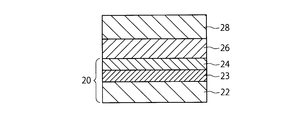
- FIG. 2 shows an example of a layer structure of a top emission type organic EL element using the electrode foil of the present invention as an anode.
- the organic EL element shown in FIG. 2 includes an electrode foil 20 as an anode provided with a metal foil 22, a reflective layer 23, and optionally a buffer layer 24, an organic EL layer 26 provided directly on the surface of the buffer layer 24, and an organic And a cathode 28 as a translucent electrode provided directly on the surface of the EL layer 26.
- the buffer layer 24 is preferably composed of a conductive amorphous carbon film or a conductive oxide film so as to be suitable as an anode.
- organic EL layer 26 various known EL layer configurations used for organic EL elements can be used. If desired, a hole injection layer and / or a hole transport layer, a light emitting layer, and an electron transport layer as required. In addition, the electron injection layer may be sequentially provided from the anode electrode foil 20 toward the cathode 28. As the hole injection layer, the hole transport layer, the light emitting layer, the electron transport layer, and the electron injection layer, layers having various known configurations and compositions can be appropriately used and are not particularly limited.
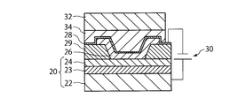
- FIG. 3 shows an example of a layer configuration of a top emission type organic EL lighting in which the organic EL element shown in FIG. 2 is incorporated.
- the organic EL element can be electrically connected to the power source 30 through the metal foil 22 of the anode electrode foil 20.
- a region of the surface of the buffer layer 24 that is not in contact with the organic EL layer 26 is covered with an interlayer insulating film 29.
- the interlayer insulating film 29 As the interlayer insulating film 29, a Si-based insulating film formed by CVD is preferable because it has a high barrier property against moisture and oxygen that cause deterioration of the organic layer, and more preferably a SiN-based insulating film.
- a more preferred interlayer insulating film is a SiNO insulating film in that the internal stress of the film is small and the flexibility is excellent.
- a sealing material 32 is provided above the cathode 28 so as to face the organic EL element, and a sealing resin 34 is filled between the sealing material 32 and the cathode 28 to form a sealing film 34.
- the sealing material 32 glass or a film can be used. In the case of glass, it can be directly bonded onto the sealing film 34 using a hydrophobic adhesive tape. In the case of a film, both surfaces and end surfaces can be covered with a Si-based insulating film. When a film having a high barrier property is developed in the future, it is possible to perform sealing without performing a coating treatment, and it is expected that the film has excellent mass productivity.
- a film is desirable from the viewpoint of imparting flexibility, but a desired performance is obtained by using a sealing material in which a film is bonded to a very thin glass having a thickness of 20 to 100 ⁇ m. It is also possible.
- cathodes used in top emission type organic EL elements can be used as the cathode 28, and since it is necessary to transmit light, it is not particularly limited as long as it is transparent or translucent. A low one is preferred.
- Preferred cathodes include conductive oxide films, magnesium-based alloy films, and fluoride films, and it is more preferable to combine these in two or more layers. These films can be the same as those described for the buffer layer of the electrode foil.
- a particularly preferable cathode has a two-layer structure in which a transparent oxide layer as a cathode layer made of a conductive oxide film is laminated with a semi-transmissive metal layer as a buffer layer made of a magnesium alloy film and / or a fluoride film.
- a transparent oxide layer as a cathode layer made of a conductive oxide film is laminated with a semi-transmissive metal layer as a buffer layer made of a magnesium alloy film and / or a fluoride film.
- the most preferred example is a cathode structure in which a transparent oxide layer (cathode layer) made of IZO (indium zinc oxide) and a semi-transmissive metal layer (buffer layer) made of Mg—Ag are laminated. Further, the cathode structure may include two or more transparent oxide layers and / or two or more semi-transmissive metal layers.
- the light generated in the organic EL layer 26 passes through the cathode 28, the sealing film 34, and the sealing material 32 and is emitted to the outside.
- assistant base material suitably in the back surface of the electrode foil 20 according to a usage form. Since this portion does not affect the light emission characteristics, the degree of freedom in material selection is high. For example, if resin films such as polyethylene terephthalate (PET), polyimide (PI), polycarbonate (PC), polyethersulfone (PES), and polyethernitrile (PEN) are used, the flexibility will not be impaired, so it is optimal. I can say that.
- PET polyethylene terephthalate
- PI polyimide
- PC polycarbonate
- PES polyethersulfone
- PEN polyethernitrile
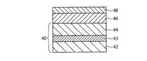
- FIG. 4 shows an example of a layer structure of a top emission type organic EL element using the electrode foil of the present invention as a cathode.
- a cathode electrode foil 40 including a metal foil 42, a reflective layer 43, and a buffer layer 44, an organic EL layer 46 provided directly on the surface of the buffer layer 44, and an organic EL layer 46.
- an anode 48 as a counter electrode provided directly on the surface.
- the organic EL layer 46 can be configured in the same manner as the organic EL layer 26 shown in FIG. 2, and the buffer layer 44 can be configured in the same manner as the cathode 28 shown in FIG. It is preferably composed of a system alloy film, a fluoride film, or a combination of two or more layers thereof.
- a more preferable buffer layer 44 is a semi-transmissive metal layer made of a magnesium-based alloy film and / or a fluoride film.
- the organic EL element using the cathode electrode foil 40 shown in FIG. 4 is the same as the organic EL element using the anode electrode foil 20 shown in FIG. 26 corresponds to a configuration in which the stacking order from the anode side to the cathode side in the interior 26 is reversed.
- a magnesium alloy film or a fluoride film is formed as the buffer layer 44 of the cathode electrode foil 40 by sputtering or vapor deposition, while a conductive amorphous carbon, MoO 3 or V 2 O 5 film is vapor deposited as the anode 48. It is preferable to form by.
- a conductive amorphous carbon film is formed on the organic EL layer, it is preferable to use a vacuum deposition method in order to avoid plasma damage during sputtering.
- a photoelectric device can be constructed on the light scattering surface.
- a photoelectric element according to a preferred embodiment of the present invention includes an electrode foil, a photoexcitation layer as a semiconductor functional layer provided directly on the surface of the electrode foil, and a translucent electrode as a counter electrode provided directly on the surface of the photoexcitation layer. Become.
- As the photoexcitation layer various structures and materials known as semiconductor functional layers of photoelectric devices can be used.
- an organic solar cell can be configured by replacing the organic EL layer 26 shown in FIG. 2 with a known organic solar cell active layer.
- a hole transport layer PEDOT: PSS (30 nm)
- a p-type organic semiconductor functional layer for example, BP (benzoic acid)
- a buffer layer for example, carbon buffer layer
- a solar cell can be formed by sequentially laminating a layer (for example, Mg—Ag) and a transparent electrode layer (for example, IZO).
- a metal foil 52 for example, a copper foil
- a reflective layer 53 for example, an aluminum film
- an n-type semiconductor buffer layer 54 for example, ZnO, SnO 2 , TiO 2 .
- the layer 56a (for example, P3HT: PCBM), the hole transport layer 56b (for example, PEDOT: PSS), and the electrode 58 may be sequentially stacked to constitute a solar cell.
- a known material can be appropriately used as a material constituting each of these layers, and is not particularly limited.
- the electrode used for the organic solar cell may have the same material and structure as the electrode used for the organic EL element.
- the electrode foil of the present invention is expected to improve the power generation efficiency due to light confinement due to the cavity effect by providing the reflective layer.
- the photoexcitation layer includes a plurality of known functional layers, and the lamination may be performed by sequentially laminating each phase from the electrode foil toward the counter electrode, or the electrode foil.
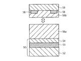
- the first stacked portion on the side and the second stacked portion on the counter electrode side are separately manufactured, and then the first and second stacked portions are bonded to each other to obtain a photoelectric device having a desired photoexcitation layer Also good. For example, as shown in FIG.
- an electrode foil 50 including a blend layer 56a of a p-type organic semiconductor and an n-type organic semiconductor is produced as a first laminated portion, while a resin film 59 (for example, polyethernitrile (PEN) ))
- PEN polyethernitrile
- a second laminated portion on which the counter electrode 58 and the hole transport layer 56b are formed is separately formed, and the blend layer 56a and the hole transport layer 56b are bonded to each other to bond the first and second layers. You may laminate
- the electrode foil 50 is prepared as a first laminated portion, while the counter electrode 58, the hole transport layer 56b and the p-type are formed on a resin film 59 (for example, polyethernitrile (PEN)).
- PEN polyethernitrile
- a second laminated portion in which an organic semiconductor and an n-type organic semiconductor blend layer 56a are formed is separately formed, and the first and second laminated layers are bonded together by bonding the blend layer 56a and the hole transport layer 56b together.
- the portions may be laminated.
- Example 1 Measurement of light scattering effect in electrode foils having various Pv / Pp ratios (1) Preparation of samples Electrode foil samples 1 to 5 having various Pv / Pp ratios were prepared. At that time, the measurement method of the surface property of each sample was as follows.
- Sample 1-Comparison In order to obtain Sample 1 provided with a standard reflective film for comparison, an aluminum film having a thickness of 200 nm was formed as a reflective layer on the surface of a quartz substrate having an arithmetic average roughness Ra of 0.2 nm by a sputtering method. In this sputtering, an Al target having a purity of 99.99% is mounted on a magnetron sputtering apparatus (MSL-464, manufactured by Tokki Co., Ltd.) connected to a cryo pump, and then input power (DC): 1000 W (3.
- MSL-464 magnetron sputtering apparatus
- Sample 2 having a low Pv / Pp ratio for comparison was prepared as follows. First, as a metal foil, a commercially available electrolytic copper foil having a thickness of 35 ⁇ m (DFF (Dual Flat Foil) manufactured by Mitsui Metal Mining Co., Ltd.) was prepared. The arithmetic average roughness Ra of the copper foil surface was 16.5 nm. The surface of the copper foil substrate was chemically polished using a chemical polishing agent (CPB-10, manufactured by Mitsubishi Gas Chemical Company), which was diluted by mixing the chemical polishing agent and water at a weight ratio of 1: 2.
- the copper foil substrate was immersed in the solution for 1 minute at room temperature, and the copper foil substrate thus treated was washed with pure water, washed with 0.1N dilute sulfuric acid, and washed again with pure water.
- an aluminum reflective layer was formed under the same conditions as in Sample 1.
- the surface property of Sample 2 obtained was measured in the same manner as Sample 1. As a result, the arithmetic average roughness Ra is 19.3 nm.
- the Pv / Pp ratio was 1.86.
- Sample 3 having a Pv / Pp ratio within the scope of the present invention was prepared as follows. First, as the metal foil, a commercially available electrolytic copper foil having a thickness of 35 ⁇ m (DFF (Dual Flat Foil) manufactured by Mitsui Metal Mining Co., Ltd.) was prepared. The surface of this copper foil was subjected to CMP treatment using a polishing machine manufactured by MT Corporation. This CMP treatment was performed for 40 seconds under the conditions of pad rotation speed: 30 rpm, load: 200 gf / cm 2 , and liquid supply amount: 100 cc / min using a polishing pad with XY grooves and a colloidal silica-based polishing liquid.
- DFF Double Flat Foil
- the arithmetic average roughness Ra of the CMP-treated copper foil surface was 6.2 nm, and the copper foil surface was applied for 20 minutes at a high frequency output of 60 W using a flowing water type ultrasonic cleaner (manufactured by Honda Electronics Co., Ltd.).
- a flowing water type ultrasonic cleaner manufactured by Honda Electronics Co., Ltd.
- an aluminum reflective layer was formed under the same conditions as in Sample 1.
- the surface properties of Sample 3 thus obtained were measured.
- the average roughness Ra is 16.2 nm, Pv / Pp ratio was 2.14.
- Sample 4 having a Pv / Pp ratio within the scope of the present invention was prepared as follows. First, as the metal foil, a commercially available electrolytic copper foil having a thickness of 35 ⁇ m (DFF (Dual Flat Foil) manufactured by Mitsui Metal Mining Co., Ltd.) was prepared. The surface of this copper foil was subjected to CMP treatment using a polishing machine manufactured by MT Corporation. This CMP treatment was performed for 60 seconds under the conditions of pad rotation speed: 30 rpm, load: 200 gf / cm 2 , and liquid supply amount: 100 cc / min, using a polishing pad with XY grooves and a colloidal silica-based polishing liquid.
- DFF Double Flat Foil
- the arithmetic average roughness Ra of the CMP-treated copper foil surface was 3.1 nm, and the copper foil surface was applied for 10 minutes at a high frequency output of 60 W using a flowing water ultrasonic cleaner (manufactured by Honda Electronics Co., Ltd.).
- An aluminum reflective layer was formed on the polished and surface-modified surface under the same conditions as in Sample 1. The properties of the surface of Sample 4 thus obtained were measured.
- the average roughness Ra is 6.1 nm, Pv / Pp ratio was 2.54.
- Sample 4 having a Pv / Pp ratio within the scope of the present invention was prepared as follows. First, as the metal foil, a commercially available electrolytic copper foil having a thickness of 35 ⁇ m (DFF (Dual Flat Foil) manufactured by Mitsui Metal Mining Co., Ltd.) was prepared. The surface of this copper foil was subjected to CMP treatment using a polishing machine manufactured by MT Corporation. This CMP treatment was performed for 40 seconds under the conditions of pad rotation speed: 30 rpm, load: 200 gf / cm 2 , and liquid supply amount: 100 cc / min using a polishing pad with XY grooves and a colloidal silica-based polishing liquid.
- DFF Double Flat Foil
- the arithmetic average roughness Ra of the CMP-treated copper foil surface was 6.8 nm, and the surface of the copper foil was applied for 10 minutes with a high-frequency output of 60 W using a flowing water ultrasonic cleaner (manufactured by Honda Electronics Co., Ltd.).
- An aluminum reflective layer was formed on the polished and surface-modified surface under the same conditions as in Sample 1. The properties of the surface of Sample 5 thus obtained were measured.
- the average roughness Ra is 13.7 nm, Pv / Pp ratio was 4.9.
- the evaluation of the light scattering effect is made with respect to the reflection angles of 10 °, 30 °, and 60 °, where the positive absolute reflectance of sample 1 as a standard reflection film is 1, and the positive absolute reflectance of samples 2 to 5 is relatively
- the positive and absolute reflectance values of Samples 2 to 5 were measured, and a value obtained by dividing the value by the positive and absolute reflectance value of the standard reflective film (Sample 1) was calculated as a light scattering relative value. Therefore, the larger the light scattering relative value, the better the light scattering effect.
- the reflective layer of each sample is made of the same material (aluminum film having a purity of 99.99%) and substantially the same film thickness (200 nm ( ⁇ 5%)). The light absorption conditions caused by the thickness were made to match.
- the sample size was 80 mm ⁇ 80 mm square.
- the light scattering relative values obtained for each sample were as shown in Tables 1 to 3 below.
- Example 2 Production and Evaluation of Electrode Foil with Various Surface Properties
- An electrode foil was prepared.
- the light scattering characteristics of these electrode foils were evaluated in the same manner as in Example 1, as shown in FIG. 8, the light scattering characteristics of all samples having a Pv / Pp ratio of 2.0 or more were improved by 1.2 times.
- samples having a Pv / Pp ratio of less than 2.0 did not have such a high light scattering property.
- a light emitting element or a power generation element was produced using these electrode foils, as shown in FIG.
- the surface profile shown in FIGS. 10 and 11 relates to the sample 6 in which the light scattering effect is improved according to the present invention, and is a desirable surface profile in which the formation of the convex portion is suppressed and the concave portion is formed preferentially.
- the surface profiles shown in FIGS. 12 and 13 relate to the sample 7 which was poor in improving the light scattering effect.
- Example 3 Evaluation of Photoelectric Characteristics (1) Production of Photoelectric Element As shown in FIG. 14, samples 6 and 7 having an aluminum reflective layer 83 on a copper foil 82 obtained as an electrode foil in Example 2 were used. Thus, a photoelectric element was manufactured. First, an n-type semiconductor buffer layer 84 made of ZnO and having a thickness of 20 nm was formed on the aluminum reflective layer 83 by sputtering. On the buffer layer 84, an interlayer insulating film made of silicon nitride was formed using a plasma CVD apparatus (manufactured by Samco, PD-2202L).
- a plurality of thin glasses having a thickness of 0.1 mm, a width of 2 mm, and a length of 10 mm were arranged on the electrode foil so as to have a width of 2 mm, thereby covering a portion to be a light receiving portion.
- the thin glass was removed. Thereafter, the electrode foil 80 was washed with an isopropyl alcohol solution heated to 40 to 50 ° C. and dried using nitrogen gas.
- PEDOT: PSS (poly (3,4-ethylenedioxythiophene / poly (4-styrenesulfonate)) dispersion (1.3 wt%) was spin coated on the electrode foil at 5000 rpm.
- the PEDOT: PSS layer 86b was obtained by drying on a hot plate for 30 minutes, and a counter electrode 88a was obtained by depositing gold so as to have a thickness of about 100 nm using a vacuum deposition apparatus.
- the portion that should become the light receiving portion was not shielded by using a comb-shaped metal mask, and was then baked in an inert atmosphere (nitrogen) at 150 ° C. for 30 minutes, as shown in FIG. A photoelectric element was obtained.
- the sample 6 with a high Pv / Pp ratio has a significantly higher fill factor FF and conversion efficiency ⁇ than the sample 7 with a low Pv / Pp ratio. It can be seen that is far superior.
- Example 4 Production and Evaluation of Electrode Foil Only for Concave Parts Sample 2 except that a commercially available electrolytic copper foil (Mitsui Metal Mining Co., Ltd., 3EC-III) with a thickness of 35 ⁇ m was used as the metal foil and the CMP treatment was performed for 2 minutes
- An electrode foil was prepared in the same manner as described above to obtain Sample 8.
- SEM SEM
- a surface property having substantially only concave portions was observed as shown in FIG.
- the surface profile was measured with the non-contact surface shape measuring machine (NewView5032, the product made by Zygo) about the sample 8, the profile image shown by FIG. 17 and 18 was obtained.
- the light scattering surface of the sample 8 had a highly desirable surface profile in which convex portions were substantially removed and only concave portions were formed.
- Most of the observed recesses had a depth of 1 ⁇ m or less and a longitudinal length of 100 ⁇ m or less.
- the number of the recesses was counted in the field of view of SEM 1000 times (10000 ⁇ m 2 ), it was about 170.
- it is possible to exhibit more excellent light scattering properties while more reliably preventing a short circuit between the electrodes, thereby improving luminous efficiency and The power generation efficiency can be further improved.
Landscapes
- Physics & Mathematics (AREA)
- Optics & Photonics (AREA)
- Electroluminescent Light Sources (AREA)
- Photovoltaic Devices (AREA)
- Electrodes Of Semiconductors (AREA)
- Led Devices (AREA)
Abstract
L'invention concerne une feuille d'électrode qui permet, tout en évitant les courts-circuits entre électrodes, d'effectuer une diffusion de lumière supérieure. Cette feuille d'électrode comprend une feuille métallique d'une épaisseur de 1-250 µm. Cette feuille d'électrode comprend, sur au moins sa surface la plus à l'extérieur, une face de diffusion de lumière dans laquelle le rapport Pv/Pp de la vallée maximale (Pv) au pic maximal (Pp) d'une courbe de section transversale mesurée pour une région rectangulaire de 181µm * 136µm en fonction de JIS B 0601-2001, est de 2,0 ou plus.
Priority Applications (2)
| Application Number | Priority Date | Filing Date | Title |
|---|---|---|---|
| US13/981,804 US9029885B2 (en) | 2012-04-23 | 2012-12-26 | Electrode foil and electronic device |
| EP12875694.7A EP2844038B1 (fr) | 2012-04-23 | 2012-12-26 | Feuille d'électrode et dispositif électronique |
Applications Claiming Priority (2)
| Application Number | Priority Date | Filing Date | Title |
|---|---|---|---|
| JP2012-097854 | 2012-04-23 | ||
| JP2012097854A JP5297546B1 (ja) | 2012-04-23 | 2012-04-23 | 電極箔及び電子デバイス |
Publications (1)
| Publication Number | Publication Date |
|---|---|
| WO2013161129A1 true WO2013161129A1 (fr) | 2013-10-31 |
Family
ID=49396810
Family Applications (1)
| Application Number | Title | Priority Date | Filing Date |
|---|---|---|---|
| PCT/JP2012/083620 Ceased WO2013161129A1 (fr) | 2012-04-23 | 2012-12-26 | Feuille d'électrode et dispositif électronique |
Country Status (5)
| Country | Link |
|---|---|
| US (1) | US9029885B2 (fr) |
| EP (1) | EP2844038B1 (fr) |
| JP (1) | JP5297546B1 (fr) |
| TW (1) | TWI508345B (fr) |
| WO (1) | WO2013161129A1 (fr) |
Cited By (1)
| Publication number | Priority date | Publication date | Assignee | Title |
|---|---|---|---|---|
| WO2020208774A1 (fr) * | 2019-04-11 | 2020-10-15 | シャープ株式会社 | Élément électroluminescent et dispositif d'affichage |
Families Citing this family (16)
| Publication number | Priority date | Publication date | Assignee | Title |
|---|---|---|---|---|
| KR101597749B1 (ko) * | 2012-07-27 | 2016-02-25 | 미쓰이금속광업주식회사 | 금속박 및 전자 디바이스 |
| JP6039540B2 (ja) * | 2013-12-13 | 2016-12-07 | 三井金属鉱業株式会社 | 電解銅箔及びその製造方法 |
| JP6431486B2 (ja) * | 2013-12-26 | 2018-11-28 | 株式会社カネカ | 太陽電池のi‐v測定方法、太陽電池のi‐v測定装置、太陽電池の製造方法、太陽電池モジュールの製造方法、および太陽電池モジュール |
| DE102014106549B4 (de) * | 2014-05-09 | 2023-10-19 | Pictiva Displays International Limited | Organisches Licht emittierendes Bauelement |
| WO2016134703A1 (fr) * | 2015-02-26 | 2016-09-01 | Dynamic Solar Systems Ag | Procédé à température ambiante pour la production de couches minces électrotechniques et succession de couches minces obtenues selon le procédé |
| MY186397A (en) * | 2015-07-29 | 2021-07-22 | Namics Corp | Roughened copper foil, copper-clad laminate, and printed wiring board |
| US20190013155A1 (en) * | 2016-02-19 | 2019-01-10 | Sekisui Chemical Co., Ltd. | Solid junction-type photovoltaic device and method for producing same |
| JP6745116B2 (ja) * | 2016-02-23 | 2020-08-26 | 積水化学工業株式会社 | フレキシブル太陽電池 |
| GB2554422A (en) * | 2016-09-27 | 2018-04-04 | Sumitomo Chemical Co | Organic microcavity photodetectors with narrow and tunable spectral response |
| JP2019536210A (ja) * | 2016-11-09 | 2019-12-12 | ケンブリッジ エンタープライズ リミティッド | リチウムイオン電池用アノード材料 |
| DE102017123154B4 (de) * | 2017-10-05 | 2025-07-03 | OSRAM Opto Semiconductors Gesellschaft mit beschränkter Haftung | Verfahren zur Herstellung eines optoelektronischen Bauelements und optoelektronisches Bauelement |
| JP7308831B2 (ja) * | 2017-12-14 | 2023-07-14 | ルミレッズ リミテッド ライアビリティ カンパニー | Ledダイの汚染を防止する方法 |
| TWI760906B (zh) * | 2020-10-28 | 2022-04-11 | 肇昇精密科技有限公司 | 預浸料製造設備及其加熱件 |
| CN114449693A (zh) * | 2020-10-30 | 2022-05-06 | 肇昇精密科技有限公司 | 预浸料制造设备及其加热件 |
| US20260059939A1 (en) * | 2022-08-22 | 2026-02-26 | Sharp Display Technology Corporation | Light-emitting element, display device, and method for manufacturing the light-emiting element |
| WO2024150719A1 (fr) * | 2023-01-10 | 2024-07-18 | 東洋紡株式会社 | Élément de conversion photoélectrique, et procédé de conversion de celui-ci |
Citations (8)
| Publication number | Priority date | Publication date | Assignee | Title |
|---|---|---|---|---|
| JP2005216705A (ja) * | 2004-01-30 | 2005-08-11 | Toppan Printing Co Ltd | 有機el表示素子およびその製造方法 |
| JP2007234254A (ja) * | 2006-02-27 | 2007-09-13 | Sanyo Electric Co Ltd | 有機エレクトロルミネッセンス素子及びその製造方法 |
| JP2008243772A (ja) | 2007-03-29 | 2008-10-09 | Seiko Epson Corp | 発光装置およびその製造方法 |
| JP2009152113A (ja) | 2007-12-21 | 2009-07-09 | Rohm Co Ltd | 有機el素子 |
| WO2011111629A1 (fr) * | 2010-03-08 | 2011-09-15 | 旭硝子株式会社 | Élément électroluminescent de del organique et son procédé de production |
| JP2011222819A (ja) | 2010-04-12 | 2011-11-04 | Mitsubishi Chemicals Corp | 太陽電池 |
| WO2011152092A1 (fr) | 2010-06-04 | 2011-12-08 | 三井金属鉱業株式会社 | Film d'électrode et dispositif organique |
| WO2011152091A1 (fr) | 2010-06-04 | 2011-12-08 | 三井金属鉱業株式会社 | Feuille d'électrode et dispositif organique |
Family Cites Families (5)
| Publication number | Priority date | Publication date | Assignee | Title |
|---|---|---|---|---|
| SE514309C2 (sv) * | 1999-05-28 | 2001-02-05 | Ericsson Telefon Ab L M | Förfarande för att bestämma ytstruktur |
| KR100975491B1 (ko) * | 2005-03-31 | 2010-08-11 | 미쓰이 긴조꾸 고교 가부시키가이샤 | 전해 동박 및 전해 동박의 제조 방법 |
| JP2006331694A (ja) * | 2005-05-23 | 2006-12-07 | Matsushita Electric Works Ltd | 有機発光素子及び有機発光素子用基板 |
| JP5016712B2 (ja) * | 2010-09-21 | 2012-09-05 | 三井金属鉱業株式会社 | 電極箔および有機デバイス |
| JP5626644B2 (ja) * | 2010-11-18 | 2014-11-19 | 三洋電機株式会社 | リチウム二次電池負極用バインダー、リチウム二次電池用負極、リチウム二次電池、リチウム二次電池負極用バインダー前駆体溶液及びリチウム二次電池用負極の製造方法 |
-
2012
- 2012-04-23 JP JP2012097854A patent/JP5297546B1/ja active Active
- 2012-12-26 EP EP12875694.7A patent/EP2844038B1/fr active Active
- 2012-12-26 US US13/981,804 patent/US9029885B2/en not_active Expired - Fee Related
- 2012-12-26 WO PCT/JP2012/083620 patent/WO2013161129A1/fr not_active Ceased
-
2013
- 2013-01-03 TW TW102100105A patent/TWI508345B/zh not_active IP Right Cessation
Patent Citations (8)
| Publication number | Priority date | Publication date | Assignee | Title |
|---|---|---|---|---|
| JP2005216705A (ja) * | 2004-01-30 | 2005-08-11 | Toppan Printing Co Ltd | 有機el表示素子およびその製造方法 |
| JP2007234254A (ja) * | 2006-02-27 | 2007-09-13 | Sanyo Electric Co Ltd | 有機エレクトロルミネッセンス素子及びその製造方法 |
| JP2008243772A (ja) | 2007-03-29 | 2008-10-09 | Seiko Epson Corp | 発光装置およびその製造方法 |
| JP2009152113A (ja) | 2007-12-21 | 2009-07-09 | Rohm Co Ltd | 有機el素子 |
| WO2011111629A1 (fr) * | 2010-03-08 | 2011-09-15 | 旭硝子株式会社 | Élément électroluminescent de del organique et son procédé de production |
| JP2011222819A (ja) | 2010-04-12 | 2011-11-04 | Mitsubishi Chemicals Corp | 太陽電池 |
| WO2011152092A1 (fr) | 2010-06-04 | 2011-12-08 | 三井金属鉱業株式会社 | Film d'électrode et dispositif organique |
| WO2011152091A1 (fr) | 2010-06-04 | 2011-12-08 | 三井金属鉱業株式会社 | Feuille d'électrode et dispositif organique |
Non-Patent Citations (1)
| Title |
|---|
| See also references of EP2844038A4 |
Cited By (1)
| Publication number | Priority date | Publication date | Assignee | Title |
|---|---|---|---|---|
| WO2020208774A1 (fr) * | 2019-04-11 | 2020-10-15 | シャープ株式会社 | Élément électroluminescent et dispositif d'affichage |
Also Published As
| Publication number | Publication date |
|---|---|
| EP2844038A1 (fr) | 2015-03-04 |
| US20140061701A1 (en) | 2014-03-06 |
| TWI508345B (zh) | 2015-11-11 |
| EP2844038A4 (fr) | 2016-01-13 |
| EP2844038B1 (fr) | 2019-05-08 |
| JP2013225447A (ja) | 2013-10-31 |
| US9029885B2 (en) | 2015-05-12 |
| JP5297546B1 (ja) | 2013-09-25 |
| TW201347256A (zh) | 2013-11-16 |
Similar Documents
| Publication | Publication Date | Title |
|---|---|---|
| JP5297546B1 (ja) | 電極箔及び電子デバイス | |
| JP6141641B2 (ja) | 電解銅箔及び電子デバイス | |
| JP5016712B2 (ja) | 電極箔および有機デバイス | |
| JP5832034B2 (ja) | 電極箔および有機デバイス | |
| WO2013118325A1 (fr) | Feuille d'électrode et dispositif électronique | |
| WO2011152092A1 (fr) | Film d'électrode et dispositif organique | |
| JP6039540B2 (ja) | 電解銅箔及びその製造方法 | |
| WO2012137525A1 (fr) | Feuille d'électrode pour dispositif organique, module de dispositif organique et son procédé de fabrication | |
| JP6134317B2 (ja) | 金属箔及び電子デバイス |
Legal Events
| Date | Code | Title | Description |
|---|---|---|---|
| WWE | Wipo information: entry into national phase |
Ref document number: 13981804 Country of ref document: US |
|
| 121 | Ep: the epo has been informed by wipo that ep was designated in this application |
Ref document number: 12875694 Country of ref document: EP Kind code of ref document: A1 |
|
| WWE | Wipo information: entry into national phase |
Ref document number: 2012875694 Country of ref document: EP |
|
| NENP | Non-entry into the national phase |
Ref country code: DE |