WO2013161146A1 - Procédé de fabrication de dispositif semi-conducteur - Google Patents
Procédé de fabrication de dispositif semi-conducteur Download PDFInfo
- Publication number
- WO2013161146A1 WO2013161146A1 PCT/JP2013/000922 JP2013000922W WO2013161146A1 WO 2013161146 A1 WO2013161146 A1 WO 2013161146A1 JP 2013000922 W JP2013000922 W JP 2013000922W WO 2013161146 A1 WO2013161146 A1 WO 2013161146A1
- Authority
- WO
- WIPO (PCT)
- Prior art keywords
- film
- dbr
- semiconductor device
- vapor deposition
- manufacturing
- Prior art date
- Legal status (The legal status is an assumption and is not a legal conclusion. Google has not performed a legal analysis and makes no representation as to the accuracy of the status listed.)
- Ceased
Links
Images


Classifications
-
- H—ELECTRICITY
- H10—SEMICONDUCTOR DEVICES; ELECTRIC SOLID-STATE DEVICES NOT OTHERWISE PROVIDED FOR
- H10F—INORGANIC SEMICONDUCTOR DEVICES SENSITIVE TO INFRARED RADIATION, LIGHT, ELECTROMAGNETIC RADIATION OF SHORTER WAVELENGTH OR CORPUSCULAR RADIATION
- H10F77/00—Constructional details of devices covered by this subclass
- H10F77/30—Coatings
- H10F77/306—Coatings for devices having potential barriers
- H10F77/331—Coatings for devices having potential barriers for filtering or shielding light, e.g. multicolour filters for photodetectors
- H10F77/337—Coatings for devices having potential barriers for filtering or shielding light, e.g. multicolour filters for photodetectors using interference filters, e.g. multilayer dielectric filters
-
- H—ELECTRICITY
- H10—SEMICONDUCTOR DEVICES; ELECTRIC SOLID-STATE DEVICES NOT OTHERWISE PROVIDED FOR
- H10F—INORGANIC SEMICONDUCTOR DEVICES SENSITIVE TO INFRARED RADIATION, LIGHT, ELECTROMAGNETIC RADIATION OF SHORTER WAVELENGTH OR CORPUSCULAR RADIATION
- H10F77/00—Constructional details of devices covered by this subclass
- H10F77/40—Optical elements or arrangements
- H10F77/42—Optical elements or arrangements directly associated or integrated with photovoltaic cells, e.g. light-reflecting means or light-concentrating means
- H10F77/48—Back surface reflectors [BSR]
-
- H—ELECTRICITY
- H01—ELECTRIC ELEMENTS
- H01S—DEVICES USING THE PROCESS OF LIGHT AMPLIFICATION BY STIMULATED EMISSION OF RADIATION [LASER] TO AMPLIFY OR GENERATE LIGHT; DEVICES USING STIMULATED EMISSION OF ELECTROMAGNETIC RADIATION IN WAVE RANGES OTHER THAN OPTICAL
- H01S5/00—Semiconductor lasers
- H01S5/02—Structural details or components not essential to laser action
- H01S5/028—Coatings ; Treatment of the laser facets, e.g. etching, passivation layers or reflecting layers
-
- H—ELECTRICITY
- H01—ELECTRIC ELEMENTS
- H01S—DEVICES USING THE PROCESS OF LIGHT AMPLIFICATION BY STIMULATED EMISSION OF RADIATION [LASER] TO AMPLIFY OR GENERATE LIGHT; DEVICES USING STIMULATED EMISSION OF ELECTROMAGNETIC RADIATION IN WAVE RANGES OTHER THAN OPTICAL
- H01S5/00—Semiconductor lasers
- H01S5/10—Construction or shape of the optical resonator, e.g. extended or external cavity, coupled cavities, bent-guide, varying width, thickness or composition of the active region
- H01S5/18—Surface-emitting [SE] lasers, e.g. having both horizontal and vertical cavities
- H01S5/183—Surface-emitting [SE] lasers, e.g. having both horizontal and vertical cavities having only vertical cavities, e.g. vertical cavity surface-emitting lasers [VCSEL]
- H01S5/18361—Structure of the reflectors, e.g. hybrid mirrors
- H01S5/18369—Structure of the reflectors, e.g. hybrid mirrors based on dielectric materials
-
- H—ELECTRICITY
- H10—SEMICONDUCTOR DEVICES; ELECTRIC SOLID-STATE DEVICES NOT OTHERWISE PROVIDED FOR
- H10H—INORGANIC LIGHT-EMITTING SEMICONDUCTOR DEVICES HAVING POTENTIAL BARRIERS
- H10H20/00—Individual inorganic light-emitting semiconductor devices having potential barriers, e.g. light-emitting diodes [LED]
- H10H20/80—Constructional details
- H10H20/84—Coatings, e.g. passivation layers or antireflective coatings
- H10H20/841—Reflective coatings, e.g. dielectric Bragg reflectors
-
- Y—GENERAL TAGGING OF NEW TECHNOLOGICAL DEVELOPMENTS; GENERAL TAGGING OF CROSS-SECTIONAL TECHNOLOGIES SPANNING OVER SEVERAL SECTIONS OF THE IPC; TECHNICAL SUBJECTS COVERED BY FORMER USPC CROSS-REFERENCE ART COLLECTIONS [XRACs] AND DIGESTS
- Y02—TECHNOLOGIES OR APPLICATIONS FOR MITIGATION OR ADAPTATION AGAINST CLIMATE CHANGE
- Y02E—REDUCTION OF GREENHOUSE GAS [GHG] EMISSIONS, RELATED TO ENERGY GENERATION, TRANSMISSION OR DISTRIBUTION
- Y02E10/00—Energy generation through renewable energy sources
- Y02E10/50—Photovoltaic [PV] energy
- Y02E10/52—PV systems with concentrators
Definitions
- the present invention relates to a method for manufacturing a light emitting device having a reflective film such as a distributed Bragg reflector, and a method for manufacturing a semiconductor device such as a method for manufacturing a light receiving device having an antireflection film on a light receiving region and on a lens.
- a reflective film such as a distributed Bragg reflector
- a semiconductor device such as a method for manufacturing a light receiving device having an antireflection film on a light receiving region and on a lens.
- FIG. 11 is a longitudinal sectional view showing a light emitting diode chip having a conventional distributed Bragg reflector disclosed in Patent Document 1.
- FIG. 11 is a longitudinal sectional view showing a light emitting diode chip having a conventional distributed Bragg reflector disclosed in Patent Document 1.
- a conventional light emitting diode chip 100 includes a substrate 101, a buffer layer 102 provided on the surface thereof, a light emitting structure 103 provided thereon, and a light emitting structure 103 on the light emitting structure 103.
- the p-electrode pad 105 provided on a part of the transparent electrode 104, and the first conductive semiconductor layer 103A of the light emitting structure 103 are exposed halfway.
- An n-electrode pad 106 provided, a distributed Bragg reflector 107 for light reflection provided on the back side of the substrate 101, a reflective metal layer 108 provided on the distributed Bragg reflector 107, and a reflective metal layer 108 and a protective layer 109 provided on 108.
- the substrate 101 is a transparent substrate, and is a sapphire substrate or a SiC substrate. As the area of the light emitting diode chip 100 is relatively large, the reflection effect increases.
- the light emitting structure 103 is made of a gallium nitride-based compound semiconductor material, that is, (Al, In, Ga) N, and includes a first conductivity type semiconductor layer 103A and a second conductivity type opposite to the first conductivity type semiconductor layer 103A.
- the semiconductor layer 103B has an active layer 103C disposed therebetween.
- compositional elements and composition ratio of the active layer 103C are determined so as to emit light having a required wavelength, for example, ultraviolet light or blue light.
- the active layer 103C may be formed in a single quantum well structure or a multiple quantum well structure.
- the light emitting structure 103 may be formed using MOCVD (metal-organic chemical vapor deposition) or MBE (molecular beam epitaxy) technology, and is used to form the n-electrode pad 106 using photolithography and etching processes.
- MOCVD metal-organic chemical vapor deposition
- MBE molecular beam epitaxy
- the first conductive type semiconductor layer 103A may be patterned so as to expose a part of the region.
- the transparent electrode layer 104 may be formed of, for example, ITO or Ni / Au on the second conductivity type semiconductor layer 103B. Since the transparent electrode layer 104 has a lower specific resistance than the second conductivity type semiconductor layer 103B, the transparent electrode layer 104 has a role of dispersing current.
- a distributed Bragg reflector 107 is disposed below the substrate 101, that is, on the back surface thereof.
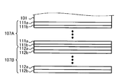
- the distributed Bragg reflector 107 includes a first distributed Bragg reflector 107A and a second distributed Bragg reflector 107B below the first distributed Bragg reflector 107A.
- FIG. 12 is a longitudinal sectional view showing details of the distributed Bragg reflector 107 of the light emitting diode chip of FIG.
- the first distributed Bragg reflector 107A of the light-emitting diode chip 100 of FIG. 11 a plurality of pairs of the first material layer 111a and the second material layer 111b are repeatedly formed.
- the second distributed Bragg reflector 107B a plurality of pairs of the third material layer 112a and the fourth material layer 112b are repeatedly formed below the second material layer 111b.
- the plurality of pairs of the first material layer 111a and the second material layer 111b have a relatively high reflectance with respect to light in the red wavelength region, for example, light at 550 nm or 630 nm, compared to light in the blue wavelength region.
- the second distributed Bragg reflector 107B has a relatively high reflectance with respect to light in the blue wavelength region, for example, light of 460 nm, compared to light in the red or green wavelength region.
- the optical film thickness of the material layers 111a and 111b in the first distributed Bragg reflector 107A is thicker than the optical film thickness of the material layers 112a and 112b in the second distributed Bragg reflector 107B. It is not limited, and may be the opposite.
- the first material layer 111a may have the same material as the third material layer 112a, that is, the same refractive index, and the second material layer 111b may be the same material as the fourth material layer 112b, that is, the same refraction. You may have a rate.
- the first material layer 11a and the third material layer 112a may be made of TiO 2 (n: about 2.5), and the second material layer 111b and the fourth material layer 112b are made of SiO 2 (n: about 2.5). 1.5).
- the optical film thickness (refractive index ⁇ thickness) of the first material layer 111a has a substantially integral multiple relationship with the optical film thickness of the second material layer 111b, and preferably these optical film thicknesses The film thickness may be substantially the same.
- the optical film thickness of the third material layer 112a has a substantially integral multiple relationship with the optical film thickness of the fourth material layer 112b, and preferably these optical film thicknesses are substantially the same. It is good.
- the optical film thickness of the first material layer 111a is made larger than the optical film thickness of the third material layer 112a
- the optical film thickness of the second material layer 111b is made larger than the optical film thickness of the fourth material layer 112b. It may be thicker.
- the optical film thickness of the first to fourth material layers 111a, 111b, 112a, 112b can be controlled by adjusting the refractive index and / or the actual thickness of each material layer.
- the conventional light emitting diode chip 100 has the distributed Bragg reflector 107 on the back surface of the substrate 101, and distributes the light emitted from the light emitting structure 103 on the front surface side of the substrate 101 to the substrate 101 side.
- a Bragg reflector 107 reflects the light to the surface side.
- the distributed Bragg reflector 107 has a multilayer structure in which low refractive index films and high refractive index films are alternately and sequentially formed.
- the distributed Bragg reflector 107 has a reflectance of 90% or more for blue, green, and red wavelength light.
- a reflective metal layer 108 is provided on the distributed Bragg reflector 107.
- the light-emitting diode chip 100 having the conventional distributed Bragg reflector 107 disclosed in Patent Document 1 needs to suppress the absorption of light at the interface between the substrate 101 and the deposited film of the distributed Bragg reflector 107.
- the vapor deposition film forming step in order to suppress light absorption at the interface between the substrate 101 and the distributed Bragg reflector 107, it is necessary to suppress the back surface contamination of the substrate 101 immediately before the vapor deposition film is formed.
- the present invention solves the above-described conventional problems, and manufactures a semiconductor device capable of efficiently suppressing contamination of a film formation surface immediately before film formation without using a dedicated cleaning device in a film formation pre-process. It aims to provide a method.
- the method for manufacturing a semiconductor device of the present invention includes an ion plasma cleaning process in which an element surface, an element back surface, an element partial side surface, or a light incident surface is subjected to ion plasma cleaning by ion plasma irradiation, the element surface, the element back surface, and the element surface.
- the film forming step in the method of manufacturing a semiconductor device according to the present invention includes forming a reflective film on the element surface, the element back surface, or the element partial side surface and / or preventing reflection on the light incident surface.
- a film is formed.
- the reflective film in the method of manufacturing a semiconductor device of the present invention is a DBR vapor deposition film, and the ion plasma irradiation is used as a film formation pretreatment cleaning before the DBR vapor deposition film or the antireflection film is formed.
- the irradiated surface is irradiated with the ion plasma.
- the DBR vapor deposition film or the antireflection film is formed on the substrate.
- the ion plasma cleaning step is performed in the same chamber of the film forming apparatus in the method for manufacturing a semiconductor device of the present invention.
- the irradiation target surface is cleaned by ionizing the element gas into an ion plasma and irradiating the irradiation target surface with plasma by a plasma source mounted inside the chamber of the film forming apparatus in the method of manufacturing a semiconductor device of the present invention. Later, the DBR deposited film or the antireflection film is formed on the irradiated surface in the chamber.
- the plasmatization is performed by using H 2 gas or O 2 gas or / and using Ar gas, He gas or N 2 gas as the element gas in the method of manufacturing a semiconductor device of the present invention.
- the ion plasma cleaning is performed with the O 2 gas flow rate of 15 to 85 sccm in the method of manufacturing a semiconductor device of the present invention.
- the ion plasma cleaning is performed with the Ar gas flow rate of 10 to 85 sccm in the method of manufacturing a semiconductor device of the present invention.
- the DBR vapor deposition film in the method for manufacturing a semiconductor device of the present invention uses a plurality of pairs of a low refractive index film and a high refractive index film.
- SiO 2 or SiO is used as the material of the low refractive index film
- TiO 2 , Ti 3 O 5 , Ti 2 O 3 is used as the material of the high refractive index film.
- TiO, ZrO 2 , TiO 2 ZrO 2 Nb 2 O 5 , or Al 2 O 3 is used.
- a pair of a high refractive index film TiO 2 and a low refractive index film SiO 2 is repeatedly formed to form a multilayer reflective film.
- the multilayer reflective film in the method for manufacturing a semiconductor device of the present invention has a number of layers in the range of 30 to 50 layers.
- the reflective film in the method for manufacturing a semiconductor device of the present invention has a reflectance in the vertical direction of 90% or more in the light wavelength range of 370 to 720 nm.
- the film forming step includes TiO 2 of a high refractive index film and SiO 2 of a low refractive index film on the element surface, the element back surface, or the element partial side surface. These pairs are repeatedly formed to form a plurality of pairs of reflective films.
- the film forming step includes an upper surface of a light receiving region in a light receiving element as the light incident surface or a surface of a lens for condensing incident light in the light receiving region.
- An antireflection film is formed on the surface.
- an ion plasma cleaning process for ion plasma cleaning of the device surface, device back surface (substrate back surface), device partial side surface or light incident surface by ion plasma irradiation, device surface, device back surface, device partial side surface or light.
- a film forming process for forming a film on the incident surface.
- the ion plasma cleaning process is performed before the film formation process, the contamination of the film formation surface immediately before the film formation is efficiently performed without using a separate dedicated cleaning apparatus for the film formation process. Can be suppressed.
- FIG. 1 It is a longitudinal cross-sectional view which shows the face-up type light emitting diode chip
- CCP capacitive coupling plasma source
- ECR electron cyclotron resonance
- FIG. 10 is a cross-sectional view showing two types of DBR deposited films on the four side surfaces in plan view of the active layer of FIG. 9 as sides of a quadrangle. It is a longitudinal cross-sectional view which shows the light emitting diode chip
- FIG. 10 is a cross-sectional view showing two types of DBR deposited films on the four side surfaces in plan view of the active layer of FIG. 9 as sides of a quadrangle.
- FIG. 1 is a longitudinal sectional view showing a face-up light emitting diode chip having a distributed Bragg reflector according to Embodiment 1 of the present invention.
- a face-up light-emitting diode chip 1 (face-up LED chip 1) as an optical semiconductor element (light-emitting element) according to the first embodiment includes an insulating substrate 2 that is a transparent substrate such as a sapphire substrate or a SiC substrate.
- the N-type cladding layer 3A provided on the surface, the active layer 3C provided thereon, the P-type cladding layer 3B provided thereon, and provided on the P-type cladding layer 3B,
- a transparent electrode 4 formed of an ITO film, a p-electrode 5 provided on a part of the transparent electrode 4, and a part of a surface exposed by removing the N-type cladding layer 3A halfway in the thickness direction It has an n-electrode 6 provided on the top and a distributed Bragg reflector 7 for light reflection provided on the back side of the substrate 2.
- a reflective metal layer may be further provided on the distributed Bragg reflector 7 (hereinafter referred to as DBR vapor deposition film 7).
- the face-up type LED chip 1 since it is necessary to output light emitted from the active layer 3 ⁇ / b> C toward the upper part of the element, light leaked to the lower side of the element is formed by the DBR vapor deposition film 17 formed on the back surface of the substrate. The light is totally reflected on the upper side of the light and output to the upper part of the element.
- the light emitting structure 3 is made of a compound semiconductor material of gallium nitride series, and the active layer 3C has a composition element and a composition ratio determined so as to emit light having a required wavelength, for example, ultraviolet light or blue light. Yes.
- the active layer 3C is formed in a single quantum well structure or a multiple quantum well structure.
- the light emitting structure 3 may be formed using MOCVD or MBE technology, and a part of the N-type cladding layer 3A is exposed to form the n-electrode 6 using photolithography and etching processes. It is patterned like this.
- the DBR vapor deposition film 7 is disposed on the back surface of the insulating substrate 2 after ion plasma cleaning is performed on the back surface of the substrate 2 to remove organic substances, moisture, and other contaminants from the back surface. That is, as shown in FIG. 2, before the DBR vapor deposition film 7 is formed, ion plasma irradiation is performed on the back surface of the insulating substrate 2 as a pre-deposition treatment cleaning. A plurality of pairs of a high refractive index film and a low refractive index film are sequentially formed as a DBR vapor deposition film 7 on the back surface of the insulating substrate 2 subjected to ion plasma cleaning.
- the manufacturing method of the face-up type LED chip 1 as the light emitting device according to the first embodiment includes an N-type cladding layer forming step of forming an N-type cladding layer 3A on the surface of the insulating substrate 2, and the N-type cladding layer 3A.
- An n-electrode forming step for forming 6 an ion plasma cleaning step for performing ion plasma cleaning on the back surface of the insulating substrate 2, and a DBR vapor deposition film forming for forming a DBR vapor deposition film 7 for light reflection on the back surface of the insulating substrate 2 And a degree.
- the processing conditions of the vapor deposition film forming apparatus are devised, and the denseness of the DBR vapor deposition film 7 is improved immediately before the DBR vapor deposition film forming process in which a plurality of pairs of high refractive index films and low refractive index films are formed.
- An ion plasma cleaning process using an ion assist gun is used.
- the ion assist gun used for improving the density of the DBR vapor deposition film 7 is diverted to the back surface of the insulating substrate 2 as an ion plasma cleaning process as a pretreatment immediately before the vapor deposition process. For this reason, it is not necessary to introduce a dedicated cleaning device or to modify the vapor deposition device, and to proceed to the formation of the DBR vapor deposition film 7 in the next DBR vapor deposition film formation step in a vacuum in the same chamber, that is, “in situ”. Can do.
- dielectric materials of a low refractive index film and a high refractive index film are used alternately.
- the order of formation may be from the high refractive index film to the low refractive index film, or vice versa.
- the dielectric material of the low refractive index film and the high refractive index film constituting the DBR vapor deposition film 7 is, for example, TiO 2 , Ti 3 O 5 , Ti 2 O 3 , TiO, ZrO 2 , TiO 2 ZrO 2 Nb. 2 O 5 , CeO 2 , ZnS, Al 2 O 3 , SiN, Nb 2 O 5 , Ta 2 O 5 , a siloxane polymer, SiO, SiO 2 , or MgF 2 may be included. Other materials may be suitable as well.
- SiO 2 or SiO is used as the material for the low refractive index film
- TiO 2 , Ti 3 O 5 , Ti 2 O 3 , TiO, ZrO 2 , TiO 2 ZrO 2 Nb 2 are used as the material for the high refractive index film.
- O 5 or Al 2 O 3 is used.
- the total number of layers is 30 or more in order to increase the reflectivity in the R, G, B visible light region.
- the multilayer reflective film When a multilayer reflective film is formed by repeatedly forming a pair of a high refractive index film of TiO 2 and a low refractive index film of SiO 2 , the multilayer reflective film has 30 to 50 layers. This reflection film has a reflectance in the vertical direction of 90% or more in the light wavelength range of 370 to 720 nm.
- the ion plasma cleaning process for performing ion plasma cleaning on the back surface of the insulating substrate 2 by ion plasma irradiation, and DBR deposition on the back surface (irradiation surface) of the insulating substrate 2 that has been subjected to ion plasma irradiation is performed.
- the DBR vapor deposition film 7 is disposed on the back surface of the insulating substrate 2.
- Light absorption at the interface between the back surface of the substrate 2 and the DBR vapor deposition film 7 is suppressed, and the reflection characteristics of the DBR vapor deposition film 7 can be improved.
- this method it becomes possible to efficiently reflect the output light from the light emitting layer (active layer 3C) of the LED device by the DBR vapor deposition film 7 under the element, and as a result, the optical element of the LED element is optically reflected.
- the brightness and / or luminous efficiency of the LED element can be increased.
- An inert gas (Ar, etc.) is ionized by a plasma source mounted in the inside of the vapor deposition apparatus processing chamber, and this is irradiated onto the back surface of the insulating substrate 2 as the target substrate, thereby cleaning the back surface of the substrate (moisture or organic matter).
- the DBR vapor deposition film 7 can be immediately formed in a vacuum by “in situ”.
- the element gas is ionized by a plasma source installed in the inside of the vapor deposition apparatus processing chamber (inside the chamber of the vapor deposition film forming apparatus), and the irradiation target surface (for example, the back surface of the substrate) is irradiated with plasma to clean the irradiation target surface. Then, a DBR vapor deposition film 7 is formed on the irradiation target surface in a vacuum in the chamber.
- H 2 gas or O 2 gas is used as elemental gas and / or plasma is formed using Ar gas, He gas or N 2 gas.
- ion plasma cleaning is performed at a gas flow rate of O 2 gas of 15 to 85 sccm.
- O 2 gas has a small atomic radius. If the O 2 gas flow rate is less than 15 sccm, the plasma does not reach the insulating substrate 2 and the organic substance removal and moisture removal effects are diminished. When the O 2 gas flow rate exceeds 85 sccm, oxidation of the back surface of the insulating substrate 2 proceeds and adversely affects the reflectance.
- ion plasma cleaning is performed at a gas flow rate of Ar gas of 10 to 85 sccm.
- Ar gas has a large atomic radius.
- the Ar gas flow rate is smaller than 10 sccm, the plasma does not reach the back surface of the insulating substrate 2 and the organic substance removing effect and the moisture removing effect are diminished.
- the Ar gas flow rate exceeds 85 sccm, Ar ions hit the back surface of the insulating substrate 2 and scrape the surface, adversely affecting the reflectance.
- the ion assist gun used for improving the density of the DBR deposited film is diverted to the ion plasma cleaning process on the back surface of the insulating substrate 2 as a pre-process immediately before the deposition, no modification is required on the hardware side of the apparatus, and the cost is reduced. Stable and low-contamination film formation can be achieved without any trouble.
- the target is a sapphire substrate, and the sapphire substrate has less plasma damage, so a higher density plasma source (ICP or the like) ) Can be applied.
- ICP higher density plasma source
- the capacitively coupled plasma source CCP discharge pressure 10 to 100 Pa, plasma density 10 to 10) shown in FIG. 10 cm ⁇ 3
- electron cyclotron resonance (ECR) plasma source discharge pressure 0.05 to 0.5 Pa, plasma density to 10 12 cm ⁇ 3
- ECR electron cyclotron resonance
- HWP discharge pressure
- ICP inductively coupled plasma source
- Plasma source SWP Surface Wave Plasma; discharge pressure 1 to 100 Pa, plasma density to 10 12 c m -3 .
- the gas species Ar, and He is H 2, O 2, N 2 .
- a grid type ion source using a DC source and a grid type ion source using an RF source have been put into practical use in existing DBR deposition apparatuses.
- Plasma sources such as CCP, ECR, HWP, ICP, and SWP are also dry-etched in order to achieve low temperature and low damage by low energy and large current ion assist method in plasma sources that are put to practical use in dry etching equipment. It may be included as a plasma source that has already been put into practical use centering on technology and can be considered as a claim for a plasma source for ion plasma cleaning which is the current claim.
- FIG. 8 is a longitudinal sectional view showing a face-down light emitting diode chip having a distributed Bragg reflector according to Embodiment 2 of the present invention.
- a face-down type light emitting diode chip 11 flip chip type LED chip 11 as an optical semiconductor element (light emitting element) of Embodiment 2 includes an insulating substrate 12 which is a transparent substrate such as a sapphire substrate or a SiC substrate.
- the flip chip type LED chip 11 it is necessary to output the light emitted from the active layer 13 ⁇ / b> C toward the lower part of the element, so that the light leaked to the upper side of the element is formed by the DBR vapor deposition film 17 formed on the upper surface of the substrate. The light is totally reflected on the lower side of the light and output to the lower part of the element.
- the N-type cladding layer 3A, the P-type cladding layer 3B, and the active layer 3C constitute a light emitting structure 13.
- the light emitting structure 13 is made of a gallium nitride-based compound semiconductor material, and the active layer 13C has a composition element and a composition ratio determined so as to emit light having a required wavelength, for example, ultraviolet light or blue light. Yes.
- the active layer 13C is formed in a single quantum well structure or a multiple quantum well structure.
- the light emitting structure 13 may be formed using MOCVD or MBE technology, and a part of the N-type cladding layer 3A is exposed to form the n-electrode 16 using photolithography and etching processes. It is patterned like this.
- the active layers 13C and P are formed from the region other than the n-electrode 16 on the exposed surface of the N-type cladding layer 13A, the region other than the p-electrode 15 on the transparent electrode 14, and the exposed side surface of the N-type cladding layer 13A.
- a series of side surfaces of the mold cladding layer 13B and the transparent electrode 14 are ion plasma cleaned to remove organic substances, moisture, and other contaminants from the back surface thereof, and then a DBR vapor deposition film 17 is disposed thereon.
- the DBR vapor deposition film 17 forms a plurality of pairs of a high refractive index film and a low refractive index film.
- the manufacturing method of the flip chip type LED chip 11 as the light emitting device of the second embodiment includes an N type clad layer forming step of forming an N type clad layer 13A on the surface of the insulating substrate 12, and the N type clad layer 13A.
- N electrode forming step for forming 16, a region other than n electrode 16 on the exposed surface of N-type cladding layer 13 A, a region other than p-electrode 15 on transparent electrode 14, and exposure of N-type cladding layer 13 A
- An ion plasma cleaning process for ion plasma cleaning a series of side surfaces of the active layer 13C, the P-type cladding layer 13B and the transparent electrode 14 from the surface, and a region on the exposed surface of the N-type cladding layer 13A other than the n electrode 16 is transparent.
- a DBR deposited film 17 for light reflection is formed on a region other than the p-electrode 15 on the electrode 14 and on a series of side surfaces of the active layer 13C, the P-type cladding layer 13B, and the transparent electrode 14 from the exposed side surface of the N-type cladding layer 13A. And a DBR vapor deposition film forming step to be formed.
- the processing conditions of the vapor deposition film forming apparatus are devised, and the denseness of the DBR vapor deposition film 17 is improved immediately before the DBR vapor deposition film forming process in which a plurality of pairs of high refractive index films and low refractive index films are formed.
- An ion plasma cleaning process using an ion assist gun is used.
- the ion assist gun used for improving the density of the DBR deposited film 17 is diverted as an ion plasma cleaning process for the element surface as a pre-process immediately before the deposition process. For this reason, it is not necessary to introduce a dedicated cleaning device or to modify the vapor deposition device, and to proceed to the formation of the DBR vapor deposition film 17 in the next DBR vapor deposition film forming step in a vacuum in the same chamber, that is, “in situ”. Can do.
- the film formation of the DBR vapor deposition film 17 can be performed immediately while maintaining the cleanliness of the element surface which is the base surface, leading to stabilization of interface control between the element surface and the DBR vapor deposition film 17.
- the element surface which is the base surface, refers to the region other than the n-electrode 16 on the exposed surface of the N-type cladding layer 13A, the region other than the p-electrode 15 on the transparent electrode 14, and the exposure of the N-type cladding layer 13A. From the side surface, it is on a series of side surfaces of the active layer 13 ⁇ / b> C, the P-type cladding layer 13 ⁇ / b> B, and the transparent electrode 14.
- dielectric materials of a low refractive index film and a high refractive index film are used alternately.
- the order of formation may be from the high refractive index film to the low refractive index film, or vice versa.
- the dielectric material of the low refractive index film and the high refractive index film constituting the DBR vapor deposition film 17 is, for example, TiO 2 , Ti 3 O 5 , Ti 2 O 3 , TiO, ZrO 2 , TiO 2 ZrO 2 Nb. 2 O 5 , CeO 2 , ZnS, Al 2 O 3 , SiN, Nb 2 O 5 , Ta 2 O 5 , a siloxane polymer, SiO, SiO 2 , or MgF 2 may be included. Other materials may be suitable as well.
- SiO 2 or SiO is used as the material for the low refractive index film
- TiO 2 , Ti 3 O 5 , Ti 2 O 3 , TiO, ZrO 2 , TiO 2 ZrO 2 Nb 2 are used as the material for the high refractive index film.
- O 5 or Al 2 O 3 is used.
- the total number of layers is 30 or more in order to increase the reflectivity in the R, G, B visible light region.
- a multilayer reflective film is formed by repeatedly forming a pair of a high refractive index film of TiO 2 and a low refractive index film of SiO 2 , the multilayer reflective film has 30 to 50 layers.
- This reflection film has a reflectance in the vertical direction of 90% or more in the light wavelength range of 370 to 720 nm.
- the DBR deposition film 17 is formed on the element surface. Since it is disposed on the surface, light absorption at the interface between the base film on the element surface and the DBR vapor deposition film 17 is suppressed, and the reflection characteristics of the DBR vapor deposition film 17 can be improved. Thus, by using this method, it becomes possible to efficiently reflect the output light from the light emitting layer (active layer 13C) of the LED device by the DBR vapor deposition film 17, resulting in the optical loss of the LED element. The brightness and / or the light emission efficiency of the LED element can be increased. Thus, the DBR vapor deposition film 17 on the surface of the element totally reflects the lower side of the element and outputs light toward the lower part of the element.
- An inert gas (Ar, etc.) is turned into ion plasma by a plasma source mounted inside the processing chamber of the vapor deposition apparatus, and this is irradiated onto the underlying film on the surface of the element, thereby cleaning the underlying film on the surface of the element (decomposing moisture and organic matter)
- the DBR vapor deposition film 17 can be immediately formed “in situ” in a vacuum after the sublimation.
- the ion assist gun used to improve the density of the DBR deposited film is diverted to the ion plasma cleaning process for the underlying film on the element surface as a pre-treatment just before the deposition, no hardware modifications are required and the cost Stable and low-contamination film formation can be achieved without any trouble.
- a lower density plasma source is considered in consideration of damage to the underlying film of GaN or ITO. Etc. must be applied.
- FIG. 9 is a longitudinal sectional view showing a semiconductor laser chip having a distributed Bragg reflector according to Embodiment 3 of the present invention.
- a semiconductor laser chip 21 as an optical semiconductor element (light emitting element) of Embodiment 3 has a double hetero structure, an N-type substrate 22, an N-type cladding layer 23 provided on the surface thereof, An active layer 24 provided thereon, a P-type cladding layer 25 provided thereon, an upper P electrode 26 provided on the P-type cladding layer 25, and a back surface of the N-type substrate 22.
- the lower N electrode 27, the DBR vapor deposition film 28 constituting the total reflection surface provided to cover the three side surfaces of the active layer 24, and the semi-reflection surface provided to cover the remaining one side surface of the active layer 24 are provided.
- a DBR vapor deposition film 29 is provided.
- one side of the side surface of the active layer 24 formed by cleavage is a semi-reflecting mirror (half mirror), and the other side facing this is a mirror surface that totally reflects.
- Various types of DBR vapor deposition films 28 and 29 are formed on the side surfaces of the active layer. The ion plasma cleaning of this method is applied to any of the DBR deposited films 28 and 29.
- the DBR vapor deposition film 28 constituting the total reflection surface is formed by the vapor deposition film forming apparatus so as to cover the three side surfaces corresponding to the adjacent three sides of the quadrangular shape of the active layer 24. Further, as shown in FIG. 10, a DBR vapor deposition film 29 constituting a semi-reflective surface is formed so as to cover the remaining one side surface corresponding to one side of the quadrangular shape of the active layer 24 in plan view. Immediately before forming these DBR vapor deposition film 28 and DBR vapor deposition film 29, ion plasma cleaning is performed on each side surface to remove organic substances, moisture, and other contaminants on each side surface from the side surfaces.
- DBR vapor deposition films 28 and 29 are formed on each cleaned side surface.
- the DBR vapor deposition films 28 and 29 also form a plurality of pairs of high refractive index films and low refractive index films.
- the manufacturing method of the semiconductor laser chip 21 as the light emitting device of Embodiment 3 includes an N-type cladding layer forming step of forming an N-type cladding layer 23 on the surface of the N-type substrate 22, and an N-type cladding layer 23 on the N-type cladding layer 23.
- a DBR vapor deposition film forming step of forming the DBR vapor deposition film 28 on three consecutive side surfaces of the side surfaces and forming the DBR vapor deposition film 29 on the remaining one side surface is provided.
- the processing conditions of the vapor deposition film forming apparatus (DBR vapor deposition film forming apparatus) are devised, immediately before the DBR vapor deposition film forming process for forming a plurality of pairs of high refractive index films and low refractive index films, An ion plasma cleaning process using an ion assist gun, which is used to improve the density of the DBR deposited films 28 and 29, is introduced.
- the ion assist gun used for improving the density of the DBR vapor deposition films 28 and 29 is diverted as an ion plasma cleaning process for the four side surfaces of the active layer 24 as a pre-process immediately before the vapor deposition process. For this reason, it is not necessary to introduce a dedicated cleaning device or to modify the vapor deposition device, and to form the DBR vapor deposition films 28 and 29 in the next DBR vapor deposition film formation step in a vacuum in the same chamber, that is, “in situ”. You can go forward.
- the element surface which is the base surface, refers to the region other than the n-electrode 16 on the exposed surface of the N-type cladding layer 13A, the region other than the p-electrode 15 on the transparent electrode 14, and the exposure of the N-type cladding layer 13A. From the side surface, it is on a series of side surfaces of the active layer 13 ⁇ / b> C, the P-type cladding layer 13 ⁇ / b> B, and the transparent electrode 14.
- dielectric materials of a low refractive index film and a high refractive index film are used alternately.
- the order of formation may be from the high refractive index film to the low refractive index film, or vice versa.
- the dielectric material of the low refractive index film and the high refractive index film constituting the DBR vapor deposition films 28 and 29 is, for example, TiO 2 , Ti 3 O 5 , Ti 2 O 3 , TiO, ZrO 2 , TiO 2 ZrO. 2 Nb 2 O 5 , CeO 2 , ZnS, Al 2 O 3 , SiN, Nb 2 O 5 , Ta 2 O 5 , a siloxane polymer, SiO, SiO 2 , or MgF 2 may be included. Other materials may be suitable as well.
- SiO 2 or SiO is used as the material for the low refractive index film
- TiO 2 , Ti 3 O 5 , Ti 2 O 3 , TiO, ZrO 2 , TiO 2 ZrO 2 Nb 2 are used as the material for the high refractive index film.
- O 5 or Al 2 O 3 is used.
- the total number of layers is 30 or more in order to increase the reflectivity in the R, G, B visible light region.
- a multilayer reflective film is formed by repeatedly forming a pair of a high refractive index film of TiO 2 and the low refractive index film of SiO 2 , the multilayer reflective film has 30 to 50 layers.
- This reflection film has a reflectance in the vertical direction of 90% or more in the light wavelength range of 370 to 720 nm.
- the semiconductor laser chip 21 after removing organic substances, moisture, and other contaminants on the device side surface (four side surfaces of the active layer 24) from the device side surface by ion plasma cleaning, Since the DBR vapor deposition films 28 and 29 are disposed on the side surface of the element, light absorption at the interface between the base film (active layer 24) on the side surface of the element and the DBR vapor deposition films 28 and 29 is suppressed, and the DBR vapor deposition film 28 is present. , 29 can be improved.
- the output light from the light emitting layer (active layer 24) of the laser device can be efficiently reflected by the DBR vapor deposition films 28 and 29, and as a result, the optical element of the laser element is optically reflected. Loss can be reduced and the brightness and / or luminous efficiency of the laser element can be increased. Accordingly, the DBR vapor deposition films 28 and 29 on the surface of the element totally reflect inside the active layer 24 of the laser element, and the laser light can be output from the DBR vapor deposition film 29 side of the laser element.
- An inert gas (Ar or the like) is ionized into plasma by a plasma source mounted in the inside of the vapor deposition apparatus processing chamber, and this is irradiated to the underlying film (active layer 24) on the side surface of the element, whereby the underlying film (active layer) on the side surface of the element. It is possible to proceed to the formation of the DBR deposited films 28 and 29 by “in situ” in a vacuum immediately after performing the cleaning of 24) (decomposition of water and organic substances, sublimation).
- the ion assist gun used for improving the density of the DBR deposited films 28 and 29 is used as an ion plasma cleaning process for the base film (active layer 24) on the side surface of the element as a pre-process immediately before the deposition, Therefore, stable and low-contamination film formation is possible without cost and without cost.
- the GaN damage of the base film (the active layer 24) is taken into consideration, so that the lower It is necessary to apply a plasma source with a density (such as RF).
- pretreatment conditions in the vapor deposition film forming device By controlling the pretreatment conditions in the vapor deposition film forming device, light absorption at the substrate / deposition layer interface, GaN or ITO / deposition layer interface and active layer / deposition layer interface can be suppressed and high reflectivity can be realized. it can.
- pre-processing conditions in-situ ion plasma (using an inert gas such as Ar) is adopted, but the plasma method (RF, ICP, etc.) is not limited, and as described above, face up
- the present invention can also be applied to element backside vapor deposition in the LED chip 1, element surface vapor deposition in the flip chip LED chip 11, and side surface vapor deposition of the semiconductor laser chip 21.
- a DBR vapor deposition film is formed as a reflective film on the light emitting element surface, the light emitting element back surface (the back surface of the insulating substrate 2), or a partial side surface of the light emitting element (side surface of the active layer 24)
- a DBR vapor deposition film is formed as a reflective film on the light emitting element surface, the light emitting element back surface (the back surface of the insulating substrate 2), or a partial side surface of the light emitting element (side surface of the active layer 24)
- an antireflection film is formed on the light incident surface of the light receiving element, that is, the upper surface of the light receiving region and / or the upper surface of the microlens (lens).
- the present invention is applied in which an antireflection film is formed after removing contaminants on the upper surface of the light receiving region and / or the upper surface of the microlens (lens) as a light incident surface of the light receiving element by ion plasma cleaning.
- the object of the present invention is achieved, which efficiently suppresses contamination of the film formation surface immediately before film formation without using a separate dedicated cleaning apparatus in the film formation pre-process. It is possible.
- a method of manufacturing a light receiving element as a semiconductor device includes an ion plasma cleaning process in which a light incident surface is ion plasma cleaned by ion plasma irradiation, and the light incident surface is incident on the upper surface of the light receiving region of the light receiving element and / or the light receiving region.
- ion plasma irradiation is used as pre-deposition cleaning before forming the antireflection film.
- the light is reflected on the irradiated surface irradiated with the ion plasma.
- a prevention film is formed.
- the present invention performs an ion plasma cleaning process before the film forming process, and is therefore dedicated to the pre-deposition process. Without using this cleaning device, it is possible to effectively suppress the backside contamination of the substrate immediately before the formation of the deposited film.
Landscapes
- Led Devices (AREA)
Abstract
Le problème décrit par la présente invention est de réduire au minimum de façon efficace la contamination d'une surface de formation de film immédiatement avant la formation du film, sans l'utilisation d'un dispositif de nettoyage spécialisé pendant le prétraitement de formation. La solution selon l'invention consiste en un procédé qui comprend les étapes suivantes : une étape de nettoyage par plasma ionique permettant un nettoyage par plasma ionique au moyen d'une exposition à un plasma ionique de la surface arrière d'un substrat isolant (2) ; et une étape de formation d'un film de dépôt DBR permettant la formation d'un film de dépôt DBR (7) sur la surface arrière (surface exposée) du substrat isolant (2) ayant subi l'exposition au plasma ionique. De cette manière, le film de dépôt DBR (7) est formé sur la surface arrière du substrat isolant (2) après que la matière organique, l'humidité et d'autres substances contaminantes ont été éliminées de la surface arrière du substrat isolant (2) par nettoyage par plasma ionique.
Applications Claiming Priority (2)
| Application Number | Priority Date | Filing Date | Title |
|---|---|---|---|
| JP2012101453 | 2012-04-26 | ||
| JP2012-101453 | 2012-04-26 |
Publications (1)
| Publication Number | Publication Date |
|---|---|
| WO2013161146A1 true WO2013161146A1 (fr) | 2013-10-31 |
Family
ID=49482504
Family Applications (1)
| Application Number | Title | Priority Date | Filing Date |
|---|---|---|---|
| PCT/JP2013/000922 Ceased WO2013161146A1 (fr) | 2012-04-26 | 2013-02-20 | Procédé de fabrication de dispositif semi-conducteur |
Country Status (2)
| Country | Link |
|---|---|
| TW (1) | TW201349537A (fr) |
| WO (1) | WO2013161146A1 (fr) |
Cited By (5)
| Publication number | Priority date | Publication date | Assignee | Title |
|---|---|---|---|---|
| US9705044B2 (en) | 2013-02-07 | 2017-07-11 | Sharp Kabushiki Kaisha | Semiconductor device and method for manufacturing same |
| JP2018137462A (ja) * | 2014-02-24 | 2018-08-30 | オスラム オプト セミコンダクターズ ゲゼルシャフト ミット ベシュレンクテル ハフツングOsram Opto Semiconductors GmbH | 被覆されたレーザファセットを有するレーザダイオードチップ |
| CN114464756A (zh) * | 2022-02-09 | 2022-05-10 | 安徽秀朗新材料科技有限公司 | 一种oled器件及其制备方法 |
| JP2023525648A (ja) * | 2020-04-21 | 2023-06-19 | ジェイド バード ディスプレイ(シャンハイ) リミテッド | 反射要素を有する発光ダイオードチップ構造 |
| JP2023527963A (ja) * | 2020-06-03 | 2023-07-03 | ジェイド バード ディスプレイ(シャンハイ) リミテッド | 水平発光を用いるマルチカラーledピクセルユニットのシステム及び方法 |
Families Citing this family (1)
| Publication number | Priority date | Publication date | Assignee | Title |
|---|---|---|---|---|
| US9490409B2 (en) | 2011-10-24 | 2016-11-08 | Formosa Epitaxy Incorporation | Light emmiting diode chip |
Citations (4)
| Publication number | Priority date | Publication date | Assignee | Title |
|---|---|---|---|---|
| JP2000164969A (ja) * | 1998-11-27 | 2000-06-16 | Matsushita Electronics Industry Corp | 半導体レーザの製造方法 |
| JP2007165711A (ja) * | 2005-12-15 | 2007-06-28 | Sharp Corp | 窒化物半導体レーザ素子 |
| JP2008300562A (ja) * | 2007-05-30 | 2008-12-11 | Sumitomo Electric Ind Ltd | Iii族窒化物半導体層貼り合わせ基板および半導体デバイス |
| JP2010056242A (ja) * | 2008-08-27 | 2010-03-11 | Shimadzu Corp | 反射防止膜成膜方法および反射防止膜成膜装置 |
-
2013
- 2013-02-20 WO PCT/JP2013/000922 patent/WO2013161146A1/fr not_active Ceased
- 2013-04-02 TW TW102111948A patent/TW201349537A/zh unknown
Patent Citations (4)
| Publication number | Priority date | Publication date | Assignee | Title |
|---|---|---|---|---|
| JP2000164969A (ja) * | 1998-11-27 | 2000-06-16 | Matsushita Electronics Industry Corp | 半導体レーザの製造方法 |
| JP2007165711A (ja) * | 2005-12-15 | 2007-06-28 | Sharp Corp | 窒化物半導体レーザ素子 |
| JP2008300562A (ja) * | 2007-05-30 | 2008-12-11 | Sumitomo Electric Ind Ltd | Iii族窒化物半導体層貼り合わせ基板および半導体デバイス |
| JP2010056242A (ja) * | 2008-08-27 | 2010-03-11 | Shimadzu Corp | 反射防止膜成膜方法および反射防止膜成膜装置 |
Cited By (6)
| Publication number | Priority date | Publication date | Assignee | Title |
|---|---|---|---|---|
| US9705044B2 (en) | 2013-02-07 | 2017-07-11 | Sharp Kabushiki Kaisha | Semiconductor device and method for manufacturing same |
| JP2018137462A (ja) * | 2014-02-24 | 2018-08-30 | オスラム オプト セミコンダクターズ ゲゼルシャフト ミット ベシュレンクテル ハフツングOsram Opto Semiconductors GmbH | 被覆されたレーザファセットを有するレーザダイオードチップ |
| US11695251B2 (en) | 2014-02-24 | 2023-07-04 | Osram Oled Gmbh | Laser diode chip having coated laser facet |
| JP2023525648A (ja) * | 2020-04-21 | 2023-06-19 | ジェイド バード ディスプレイ(シャンハイ) リミテッド | 反射要素を有する発光ダイオードチップ構造 |
| JP2023527963A (ja) * | 2020-06-03 | 2023-07-03 | ジェイド バード ディスプレイ(シャンハイ) リミテッド | 水平発光を用いるマルチカラーledピクセルユニットのシステム及び方法 |
| CN114464756A (zh) * | 2022-02-09 | 2022-05-10 | 安徽秀朗新材料科技有限公司 | 一种oled器件及其制备方法 |
Also Published As
| Publication number | Publication date |
|---|---|
| TW201349537A (zh) | 2013-12-01 |
Similar Documents
| Publication | Publication Date | Title |
|---|---|---|
| US6570186B1 (en) | Light emitting device using group III nitride compound semiconductor | |
| CN101512783B (zh) | 半导体发光元件 | |
| JP5728116B2 (ja) | Led素子及びその製造方法 | |
| WO2013161146A1 (fr) | Procédé de fabrication de dispositif semi-conducteur | |
| KR102443027B1 (ko) | 반도체 발광소자 | |
| US9419185B2 (en) | Method of singulating LED wafer substrates into dice with LED device with Bragg reflector | |
| US8390007B2 (en) | Semiconductor light emitting device and method of fabricating semiconductor light emitting device | |
| KR20190104692A (ko) | 반도체 발광소자 | |
| CN108682727B (zh) | 一种发光二极管芯片及其制作方法 | |
| US8618564B2 (en) | High efficiency light emitting diodes | |
| JP2009164506A (ja) | 半導体発光素子 | |
| JPWO2014126016A1 (ja) | Led素子及びその製造方法 | |
| CN105938862A (zh) | 一种GaN基发光二极管芯片及其制备方法 | |
| JPH11126925A (ja) | 窒化ガリウム系化合物半導体発光素子 | |
| JP2012028773A (ja) | 半導体発光素子及びその製造方法 | |
| EP4576229A1 (fr) | Diode électroluminescente ultraviolette et son procédé de fabrication | |
| CN108231966A (zh) | 一种具有反射镜的led芯片及其制作方法 | |
| CN109509822B (zh) | 一种具有光散射结构和odr的发光二极管及其制备方法 | |
| WO2014057591A1 (fr) | Élément électroluminescent semi-conducteur et son procédé de production | |
| JP2015185655A (ja) | 発光素子およびその製造方法 | |
| US12588331B2 (en) | Selective optical filter for RGB LED | |
| CN118610338A (zh) | 一种具有倾斜侧壁和混介质层odr的深紫外发光二极管及其制备方法 | |
| JP7722624B2 (ja) | 低屈折率パターン化構造を有する薄膜ledアレイ | |
| US20110037092A1 (en) | Light-emitting element | |
| CN107968143A (zh) | 一种具有高反射率宽谱氧化物反射镜的倒装蓝光led芯片及其制备方法 |
Legal Events
| Date | Code | Title | Description |
|---|---|---|---|
| 121 | Ep: the epo has been informed by wipo that ep was designated in this application |
Ref document number: 13782355 Country of ref document: EP Kind code of ref document: A1 |
|
| NENP | Non-entry into the national phase |
Ref country code: DE |
|
| 122 | Ep: pct application non-entry in european phase |
Ref document number: 13782355 Country of ref document: EP Kind code of ref document: A1 |
|
| NENP | Non-entry into the national phase |
Ref country code: JP |