WO2013161478A1 - Élément semi-conducteur au nitrure - Google Patents
Élément semi-conducteur au nitrure Download PDFInfo
- Publication number
- WO2013161478A1 WO2013161478A1 PCT/JP2013/058598 JP2013058598W WO2013161478A1 WO 2013161478 A1 WO2013161478 A1 WO 2013161478A1 JP 2013058598 W JP2013058598 W JP 2013058598W WO 2013161478 A1 WO2013161478 A1 WO 2013161478A1
- Authority
- WO
- WIPO (PCT)
- Prior art keywords
- nitride
- layer
- substrate
- type
- semiconductor device
- Prior art date
- Legal status (The legal status is an assumption and is not a legal conclusion. Google has not performed a legal analysis and makes no representation as to the accuracy of the status listed.)
- Ceased
Links
Images





Classifications
-
- H—ELECTRICITY
- H10—SEMICONDUCTOR DEVICES; ELECTRIC SOLID-STATE DEVICES NOT OTHERWISE PROVIDED FOR
- H10D—INORGANIC ELECTRIC SEMICONDUCTOR DEVICES
- H10D30/00—Field-effect transistors [FET]
- H10D30/40—FETs having zero-dimensional [0D], one-dimensional [1D] or two-dimensional [2D] charge carrier gas channels
- H10D30/47—FETs having zero-dimensional [0D], one-dimensional [1D] or two-dimensional [2D] charge carrier gas channels having two-dimensional [2D] charge carrier gas channels, e.g. nanoribbon FETs or high electron mobility transistors [HEMT]
- H10D30/471—High electron mobility transistors [HEMT] or high hole mobility transistors [HHMT]
- H10D30/473—High electron mobility transistors [HEMT] or high hole mobility transistors [HHMT] having confinement of carriers by multiple heterojunctions, e.g. quantum well HEMT
- H10D30/4732—High electron mobility transistors [HEMT] or high hole mobility transistors [HHMT] having confinement of carriers by multiple heterojunctions, e.g. quantum well HEMT using Group III-V semiconductor material
-
- H—ELECTRICITY
- H10—SEMICONDUCTOR DEVICES; ELECTRIC SOLID-STATE DEVICES NOT OTHERWISE PROVIDED FOR
- H10D—INORGANIC ELECTRIC SEMICONDUCTOR DEVICES
- H10D30/00—Field-effect transistors [FET]
- H10D30/40—FETs having zero-dimensional [0D], one-dimensional [1D] or two-dimensional [2D] charge carrier gas channels
- H10D30/47—FETs having zero-dimensional [0D], one-dimensional [1D] or two-dimensional [2D] charge carrier gas channels having two-dimensional [2D] charge carrier gas channels, e.g. nanoribbon FETs or high electron mobility transistors [HEMT]
- H10D30/471—High electron mobility transistors [HEMT] or high hole mobility transistors [HHMT]
- H10D30/475—High electron mobility transistors [HEMT] or high hole mobility transistors [HHMT] having wider bandgap layer formed on top of lower bandgap active layer, e.g. undoped barrier HEMTs such as i-AlGaN/GaN HEMTs
- H10D30/4755—High electron mobility transistors [HEMT] or high hole mobility transistors [HHMT] having wider bandgap layer formed on top of lower bandgap active layer, e.g. undoped barrier HEMTs such as i-AlGaN/GaN HEMTs having wide bandgap charge-carrier supplying layers, e.g. modulation doped HEMTs such as n-AlGaAs/GaAs HEMTs
-
- H—ELECTRICITY
- H10—SEMICONDUCTOR DEVICES; ELECTRIC SOLID-STATE DEVICES NOT OTHERWISE PROVIDED FOR
- H10D—INORGANIC ELECTRIC SEMICONDUCTOR DEVICES
- H10D62/00—Semiconductor bodies, or regions thereof, of devices having potential barriers
- H10D62/80—Semiconductor bodies, or regions thereof, of devices having potential barriers characterised by the materials
- H10D62/81—Semiconductor bodies, or regions thereof, of devices having potential barriers characterised by the materials of structures exhibiting quantum-confinement effects, e.g. single quantum wells; of structures having periodic or quasi-periodic potential variation
- H10D62/815—Semiconductor bodies, or regions thereof, of devices having potential barriers characterised by the materials of structures exhibiting quantum-confinement effects, e.g. single quantum wells; of structures having periodic or quasi-periodic potential variation of structures having periodic or quasi-periodic potential variation, e.g. superlattices or multiple quantum wells [MQW]
- H10D62/8161—Semiconductor bodies, or regions thereof, of devices having potential barriers characterised by the materials of structures exhibiting quantum-confinement effects, e.g. single quantum wells; of structures having periodic or quasi-periodic potential variation of structures having periodic or quasi-periodic potential variation, e.g. superlattices or multiple quantum wells [MQW] potential variation due to variations in composition or crystallinity, e.g. heterojunction superlattices
- H10D62/8162—Semiconductor bodies, or regions thereof, of devices having potential barriers characterised by the materials of structures exhibiting quantum-confinement effects, e.g. single quantum wells; of structures having periodic or quasi-periodic potential variation of structures having periodic or quasi-periodic potential variation, e.g. superlattices or multiple quantum wells [MQW] potential variation due to variations in composition or crystallinity, e.g. heterojunction superlattices having quantum effects only in the vertical direction, i.e. layered structures having quantum effects solely resulting from vertical potential variation
- H10D62/8164—Semiconductor bodies, or regions thereof, of devices having potential barriers characterised by the materials of structures exhibiting quantum-confinement effects, e.g. single quantum wells; of structures having periodic or quasi-periodic potential variation of structures having periodic or quasi-periodic potential variation, e.g. superlattices or multiple quantum wells [MQW] potential variation due to variations in composition or crystallinity, e.g. heterojunction superlattices having quantum effects only in the vertical direction, i.e. layered structures having quantum effects solely resulting from vertical potential variation comprising only semiconductor materials
-
- H—ELECTRICITY
- H10—SEMICONDUCTOR DEVICES; ELECTRIC SOLID-STATE DEVICES NOT OTHERWISE PROVIDED FOR
- H10D—INORGANIC ELECTRIC SEMICONDUCTOR DEVICES
- H10D62/00—Semiconductor bodies, or regions thereof, of devices having potential barriers
- H10D62/80—Semiconductor bodies, or regions thereof, of devices having potential barriers characterised by the materials
- H10D62/82—Heterojunctions
- H10D62/824—Heterojunctions comprising only Group III-V materials heterojunctions, e.g. GaN/AlGaN heterojunctions
-
- H—ELECTRICITY
- H10—SEMICONDUCTOR DEVICES; ELECTRIC SOLID-STATE DEVICES NOT OTHERWISE PROVIDED FOR
- H10D—INORGANIC ELECTRIC SEMICONDUCTOR DEVICES
- H10D8/00—Diodes
-
- H—ELECTRICITY
- H10—SEMICONDUCTOR DEVICES; ELECTRIC SOLID-STATE DEVICES NOT OTHERWISE PROVIDED FOR
- H10W—GENERIC PACKAGES, INTERCONNECTIONS, CONNECTORS OR OTHER CONSTRUCTIONAL DETAILS OF DEVICES COVERED BY CLASS H10
- H10W40/00—Arrangements for thermal protection or thermal control
- H10W40/20—Arrangements for cooling
- H10W40/25—Arrangements for cooling characterised by their materials
- H10W40/254—Diamond
-
- H—ELECTRICITY
- H10—SEMICONDUCTOR DEVICES; ELECTRIC SOLID-STATE DEVICES NOT OTHERWISE PROVIDED FOR
- H10D—INORGANIC ELECTRIC SEMICONDUCTOR DEVICES
- H10D62/00—Semiconductor bodies, or regions thereof, of devices having potential barriers
- H10D62/80—Semiconductor bodies, or regions thereof, of devices having potential barriers characterised by the materials
- H10D62/82—Heterojunctions
-
- H—ELECTRICITY
- H10—SEMICONDUCTOR DEVICES; ELECTRIC SOLID-STATE DEVICES NOT OTHERWISE PROVIDED FOR
- H10D—INORGANIC ELECTRIC SEMICONDUCTOR DEVICES
- H10D62/00—Semiconductor bodies, or regions thereof, of devices having potential barriers
- H10D62/80—Semiconductor bodies, or regions thereof, of devices having potential barriers characterised by the materials
- H10D62/83—Semiconductor bodies, or regions thereof, of devices having potential barriers characterised by the materials being Group IV materials, e.g. B-doped Si or undoped Ge
- H10D62/8303—Diamond
-
- H—ELECTRICITY
- H10—SEMICONDUCTOR DEVICES; ELECTRIC SOLID-STATE DEVICES NOT OTHERWISE PROVIDED FOR
- H10D—INORGANIC ELECTRIC SEMICONDUCTOR DEVICES
- H10D62/00—Semiconductor bodies, or regions thereof, of devices having potential barriers
- H10D62/80—Semiconductor bodies, or regions thereof, of devices having potential barriers characterised by the materials
- H10D62/85—Semiconductor bodies, or regions thereof, of devices having potential barriers characterised by the materials being Group III-V materials, e.g. GaAs
- H10D62/8503—Nitride Group III-V materials, e.g. AlN or GaN
-
- H—ELECTRICITY
- H10—SEMICONDUCTOR DEVICES; ELECTRIC SOLID-STATE DEVICES NOT OTHERWISE PROVIDED FOR
- H10P—GENERIC PROCESSES OR APPARATUS FOR THE MANUFACTURE OR TREATMENT OF DEVICES COVERED BY CLASS H10
- H10P14/00—Formation of materials, e.g. in the shape of layers or pillars
- H10P14/20—Formation of materials, e.g. in the shape of layers or pillars of semiconductor materials
- H10P14/24—Formation of materials, e.g. in the shape of layers or pillars of semiconductor materials using chemical vapour deposition [CVD]
-
- H—ELECTRICITY
- H10—SEMICONDUCTOR DEVICES; ELECTRIC SOLID-STATE DEVICES NOT OTHERWISE PROVIDED FOR
- H10P—GENERIC PROCESSES OR APPARATUS FOR THE MANUFACTURE OR TREATMENT OF DEVICES COVERED BY CLASS H10
- H10P14/00—Formation of materials, e.g. in the shape of layers or pillars
- H10P14/20—Formation of materials, e.g. in the shape of layers or pillars of semiconductor materials
- H10P14/29—Formation of materials, e.g. in the shape of layers or pillars of semiconductor materials characterised by the substrates
- H10P14/2901—Materials
- H10P14/2902—Materials being Group IVA materials
- H10P14/2905—Silicon, silicon germanium or germanium
-
- H—ELECTRICITY
- H10—SEMICONDUCTOR DEVICES; ELECTRIC SOLID-STATE DEVICES NOT OTHERWISE PROVIDED FOR
- H10P—GENERIC PROCESSES OR APPARATUS FOR THE MANUFACTURE OR TREATMENT OF DEVICES COVERED BY CLASS H10
- H10P14/00—Formation of materials, e.g. in the shape of layers or pillars
- H10P14/20—Formation of materials, e.g. in the shape of layers or pillars of semiconductor materials
- H10P14/32—Formation of materials, e.g. in the shape of layers or pillars of semiconductor materials characterised by intermediate layers between substrates and deposited layers
- H10P14/3202—Materials thereof
- H10P14/3214—Materials thereof being Group IIIA-VA semiconductors
- H10P14/3216—Nitrides
-
- H—ELECTRICITY
- H10—SEMICONDUCTOR DEVICES; ELECTRIC SOLID-STATE DEVICES NOT OTHERWISE PROVIDED FOR
- H10P—GENERIC PROCESSES OR APPARATUS FOR THE MANUFACTURE OR TREATMENT OF DEVICES COVERED BY CLASS H10
- H10P14/00—Formation of materials, e.g. in the shape of layers or pillars
- H10P14/20—Formation of materials, e.g. in the shape of layers or pillars of semiconductor materials
- H10P14/32—Formation of materials, e.g. in the shape of layers or pillars of semiconductor materials characterised by intermediate layers between substrates and deposited layers
- H10P14/3242—Structure
- H10P14/3244—Layer structure
- H10P14/3251—Layer structure consisting of three or more layers
- H10P14/3252—Alternating layers, e.g. superlattice
-
- H—ELECTRICITY
- H10—SEMICONDUCTOR DEVICES; ELECTRIC SOLID-STATE DEVICES NOT OTHERWISE PROVIDED FOR
- H10P—GENERIC PROCESSES OR APPARATUS FOR THE MANUFACTURE OR TREATMENT OF DEVICES COVERED BY CLASS H10
- H10P14/00—Formation of materials, e.g. in the shape of layers or pillars
- H10P14/20—Formation of materials, e.g. in the shape of layers or pillars of semiconductor materials
- H10P14/34—Deposited materials, e.g. layers
- H10P14/3402—Deposited materials, e.g. layers characterised by the chemical composition
- H10P14/3414—Deposited materials, e.g. layers characterised by the chemical composition being group IIIA-VIA materials
- H10P14/3416—Nitrides
Definitions
- the present invention relates to a nitride semiconductor device, and more particularly to a nitride semiconductor device which is a GaN deelectronic device.
- a GaN-based electronic device which is a nitride-based semiconductor element, has a larger band gap energy than a GaAs-based material, has a high heat resistance, and is excellent in high-temperature operation. For this reason, development of heterojunction field effect transistors (Hetero-structure Field Effect Transistors: HFETs) using these materials, particularly GaN / AlGaN-based semiconductors, is in progress in nitride semiconductor devices.
- Si substrates are one of the promising substrates for GaN-based electronic devices because they are inexpensive and can be expected to have a large diameter.
- the epitaxial layer on the Si substrate needs to be thick in order to realize a high breakdown voltage element.
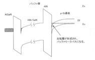
- FIG. 9 shows a band structure diagram of an example of a conventional nitride semiconductor device.
- an AlN layer is often formed on a Si substrate to avoid the reaction between Si and Ga, but as shown in FIG. 9, the interface between the Si substrate and the AlN layer of the buffer layer Point out that an inversion layer is formed. It is presumed that the inversion layer becomes a leak path, which in turn causes the breakdown voltage of the nitride semiconductor device to deteriorate.
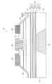
- FIG. 10 shows a cross-sectional view of an example of a schematic configuration of such a conventional nitride-based semiconductor element.
- the nitride-based semiconductor device shown in FIG. 10 has problems of deterioration of on-resistance and reliability and needs to be improved.
- An object of the present invention is to provide a nitride-based semiconductor element that has a high withstand voltage during operation and high reliability.
- a first aspect of the present invention is a nitride-based compound semiconductor device, comprising a conductive substrate, a p-type electrically conductive material provided in a partial region of the conductive substrate, the substrate, A nitride-based semiconductor layer having an electron transit layer and an electron supply layer formed on the p-type electrically conductive material, a first electrode formed on the nitride-based semiconductor layer, and the nitride-based semiconductor A second electrode formed on the layer and spaced apart from the first electrode, wherein the p-type electrically conductive material is an end of the first electrode on the nitride-based semiconductor layer on the second electrode side. And in the region of the substrate corresponding to the region between the second electrode and the end on the first electrode side of the second electrode.
- the p-type electrically conductive material is made of a material in which an inversion layer is not formed between the lowermost layer of the nitride-based semiconductor layer.
- the p-type electrically conductive material has a Fermi energy at a conduction band edge of the p-type electrically conductive material at the lowest layer of the nitride-based semiconductor layer. It is a level higher than energy by 0.1 eV or more.
- the band gap of the p-type electrically conductive material is 2 eV or more.
- the p-type electrically conductive material is made of p-type diamond.
- the p-type electrically conductive material is made of a p-type oxide semiconductor.
- the p-type oxide semiconductor is made of any one of Cu 2 O, CuAlO 2 , ZnRh 2 O 4 , NiO x , and GaN.
- the substrate is a Si substrate, a SiC substrate, and an i-type or n-type conductive oxide substrate.
- the ninth aspect of the present invention is the diode according to any one of the above aspects.
- a tenth aspect of the present invention is a transistor according to any one of the first to eighth aspects.
- the present embodiment is an example of the nitride-based semiconductor element of the present invention, and the present invention is not limited to the present embodiment.
- the nitride semiconductor device of the present invention is a diode
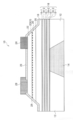
- FIG. 1A shows a cross-sectional view of a schematic configuration of a GaN-based diode of this example.
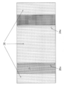
- FIG. 1B shows a schematic top view of the GaN-based diode of the example.
- the nitride semiconductor device 10 includes a substrate 12, a p-type semiconductor 14, a buffer layer 16, a high resistance layer 18, a channel layer 20, a barrier layer 22, a cathode electrode 24, an anode electrode 26, And an insulating film 28.
- the substrate 12 is a conductive substrate made of silicon (Si) having a (111) plane as a main surface.
- the substrate 12 of this embodiment is etched along a position corresponding to the end of the anode electrode 26, and a wide band gap (WBG) p-type semiconductor (p-type semiconductor 14) is embedded therein.
- the p-type semiconductor 14 of this embodiment has a function of cutting off a leak path of a leak current (buffer leak) when the nitride semiconductor element 10 is in an off state.
- the p-type semiconductor 14 has a function of absorbing (conducting) heat generated between the cathode electrode 24 and the anode electrode 26 when the element is driven.
- the material of the p-type semiconductor 14 is a material showing a band structure in which no inversion layer is formed between the p-type semiconductor 14 and the lowermost AlN layer of the buffer layer 16. Is preferred.
- diamond is particularly preferable because of its very high thermal conductivity. Note that diamond is preferable from the viewpoint of manufacturing because it is easy to form by CVD or sputtering.
- the material of the p-type semiconductor 14 may be an oxide as long as it is a WBG semiconductor.
- the p-type semiconductor 14 is an oxide that becomes p-type such as Cu 2 O, CuAlO 2 , ZnRh 2 O 4 , and NiO x. May be.
- the buffer layer 16 formed on the substrate 12 and the p-type semiconductor 14 is a buffer layer having a stacked structure of, for example, an AlN layer 16-1 and a GaN layer 16-2.
- the high resistance layer 18 formed on the buffer layer 16 has a higher electrical resistance than the channel layer 20 and is, for example, a GaN layer (GaN: C layer) to which C is added.
- the channel layer 20 formed on the high resistance layer 18 is an undoped GaN (uid-GaN) layer.
- the channel layer 20 functions as an electron transit layer.
- the barrier layer 22 formed on the channel layer 20 is an undoped AlGaN layer (barrier layer).
- the barrier layer 22 functions as an electron supply layer.
- an undoped AlGaN layer (barrier layer 22) is heterojunction with the surface of the undoped GaN layer (channel layer 20) corresponding to the channel length L. Therefore, a two-dimensional electron gas (2DEG) is generated at the interface of the heterojunction portion.
- the two-dimensional electron gas plays a role of reducing the access resistance, and thus exhibits a low on-resistance.
- the cathode electrode 24 is formed in the order of Ti, an alloy of Al and Si, and W from a region closest to the AlGaN layer of the barrier layer 22.
- the anode 26 is formed in the order of Ni and Au from the region of the barrier layer 22 closest to the AlGaN layer.
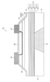
- FIG. 2 is a cross-sectional view showing an example of a schematic configuration of the nitride-based semiconductor element 10 in an on state. As shown in FIG. 2, in the on state, a current flows through the 2DEG from the anode electrode 26 toward the cathode electrode 24.
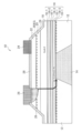
- FIG. 3 shows a cross-sectional view of a schematic configuration of the nitride semiconductor element 10 in the off state.
- the 2DEG channel is pinched off and no current flows.
- a slight leak current buffer leak
- a slight leak current tends to flow through the interface between the AlN layer 16-1 as the lowermost layer of the buffer layer 16 and the substrate 12.
- FIG. 4 shows a schematic diagram of the band structure at this time.
- an inversion layer is provided at the interface between the AlN layer, which is the lowermost layer of the buffer layer, and the substrate. Therefore, the inversion layer becomes a conductive layer and becomes a leak path.
- the p-type semiconductor 14 when the p-type semiconductor 14 is embedded in the substrate 12 as shown in FIG. 4, it is inverted to the interface between the AlN layer at the bottom of the buffer layer 16 and the substrate 12. Since no layer is formed, no leak path is formed and the leak current is very small.
- the p-type semiconductor 14 embedded in the substrate 12 is defined for the following reason from the viewpoint of preventing the inversion layer from being formed.
- the energy of the conduction band edge of the p-type semiconductor is at a level higher by 0.2 eV or more than the Fermi energy of the material constituting the lowermost layer of the semiconductor layer on the substrate, the formation of the inversion layer can be prevented more reliably. Therefore, it is more preferable.
- the band gap of the p-type semiconductor is 2 eV or more, it is possible to prevent the element from being destroyed by relaxing the electric field concentration.
- the leakage current usually varies depending on the film thickness of the buffer layer 16 when the substrate 12 is not processed.
- Table 1 shows the relationship between the film thickness (total film thickness) of the buffer layer 16 and the leakage current.
- the thickness of the buffer layer 16 is increased and the leakage current is reduced by orders of magnitude. This indicates that the leakage current in the vertical direction of the nitride-based semiconductor element 10 is suppressed by the relaxation of the electric field strength.
- the leakage current is 1 ⁇ 10 10 even when the buffer layer 16 is as thin as 2.5 ⁇ m. -7 , which is sufficiently low compared to the case where the back surface processing is not performed. Furthermore, even if the buffer layer 16 is made thicker, the leakage current gradually decreases, but it does not tend to decrease so dramatically. This means that the back surface processing of the substrate 12 can effectively suppress the leakage current even when the buffer layer 16 is thin, and the throughput is further improved.
- the p-type semiconductor 14 embedded in the substrate 12 absorbs (conducts) heat generated when the element is driven, particularly heat generated between the cathode electrode 24 and the anode electrode 26, and therefore from the viewpoint of thermal conductivity. It is prescribed.
- air space
- air does not have a high thermal conductivity, and is particularly lower than that of the p-type semiconductor 14, so that the heat generated between the cathode electrode 24 and the anode electrode 26 can be sufficiently absorbed (conducted).
- the heat generated between the cathode electrode 24 and the anode electrode 26 can be sufficiently absorbed (conducted).
- the p-type semiconductor 14 of this embodiment a case where another general insulator is provided in the substrate 12 can be considered.
- an insulator generally has a lower thermal conductivity than the p-type semiconductor 14, there is a concern that heat generated between the cathode electrode 24 and the anode electrode 26 cannot be sufficiently absorbed (conducted). There is. When the heat is not sufficiently absorbed (conducted) in this way, the nitride semiconductor device has a problem that the thermal resistance increases and the junction temperature increases, resulting in a decrease in reliability.
- the heat generated between the cathode electrode 24 and the anode electrode 26 is sufficiently absorbed (conducted) by using the p-type semiconductor 14 having a higher thermal conductivity than air or an insulator. .
- the heat generated between the cathode electrode 24 and the anode electrode 26 is sufficiently absorbed (conducted) by using the p-type semiconductor 14 having a higher thermal conductivity than air or an insulator.
- the p-type semiconductor 14 having higher thermal conductivity. Since diamond has a very high thermal conductivity, the thermal resistance can be lowered and the on-characteristics can be improved.
- the p-type semiconductor may be an oxide as long as it is a WBG semiconductor, and more effective if it is an oxide that becomes p-type, such as Cu 2 O, CuAlO 2 , ZnRh 2 O 4 , NiO x , and GaN. It is possible to suppress the leakage current.
- a material that does not form an inversion layer based on the band energy as shown in FIG. 5 may be selected, and any material having high thermal conductivity from the viewpoint of thermal resistance. More preferable.
- the growth apparatus was a MOCVD (Metal Organic Chemical Vapor Deposition) apparatus, and the substrate 12 was a silicon (111) substrate.
- MOCVD Metal Organic Chemical Vapor Deposition
- the silicon (111) substrate 12 is introduced into the MOCVD apparatus, and the vacuum degree in the MOCVD apparatus is reduced to 1 ⁇ 10 ⁇ 6 hPa or less with a turbo pump, and then the degree of vacuum is set to 100 hPa.
- the substrate 12 is heated to 1050 ° C.
- TMA trimethylaluminum
- the substrate 12 is rotated at 900 rpm, trimethylaluminum (TMA) as a raw material is introduced into the surface of the substrate 12 at a flow rate of 100 cm 3 / min, and ammonia is supplied at a flow rate of 12 liters / min.
- TMA trimethylaluminum
- the buffer layer 16 made of is epitaxially grown. The growth time is 4 min and the thickness of the buffer layer 16 is about 50 nm.
- a laminated film comprising, for example, a GaN layer 16-2 having a thickness of 5 to 100 nm and an AlN layer 16-1 having a thickness of 1 to 10 nm is formed on the AlN layer 16-1.
- 20 to 80 layers are stacked to form the buffer layer 16.
- the buffer layer 16 is not limited to this configuration, and may be variously modified depending on the material of the channel layer 20 and other conditions.
- the high resistance layer 18 is epitaxially grown on the buffer layer 16 using trimethyl gallium (TMG) as a raw material, and C is doped.
- TMG trimethyl gallium
- TMG is introduced onto the high resistance layer 182 at a flow rate of 300 cm 3 / min while flowing ammonia at a flow rate of 12 liters / min, and the channel layer 20 made of a GaN layer is epitaxially grown. .
- the channel layer 20 functions as an electron transit layer.
- the growth time of the channel layer 20 is 200 sec, and the film thickness of the channel layer 20 is 300 nm.
- TMA is introduced at a flow rate of 50 cm 3 / min
- trimethylgallium (TMG) is 100 cm 3 / min
- ammonia is introduced at a flow rate of 12 liters / min
- an Al 0.3 Ga 0.7 N layer is formed.
- the barrier layer 22 is epitaxially grown.
- the barrier layer 22 functions as an electron supply layer.
- the growth time of the barrier layer 22 is 40 sec, and the thickness of the barrier layer 22 is 30 nm.
- an isolation mesa is formed for element isolation using chlorine gas or the like.
- a portion where the cathode electrode 24 is to be formed is opened using a resist or the like to expose the surface of the barrier layer 22, and Ti, Al and Si alloy film, and W are sequentially deposited thereon to form the cathode electrode. 24 was formed by a lift-off method or the like.
- patterning is then performed using a resist or the like, and patterning is performed by providing an opening at a position where the anode electrode 26 is to be formed using a resist or the like at a position where the anode electrode 26 is to be formed, and the barrier layer 22.
- the anode electrode 26 was formed by depositing Ni or Au or the like on the surface.
- an insulating film 28 such as polyimide or SiO 2 is further deposited and patterned as an interlayer insulating film.
- gold plating or a thick Al film is deposited on the cathode electrode 24 and the anode electrode 26 in order to reduce the metal resistance (not shown).
- an insulating film such as polyimide or SiO 2 is deposited to form a passivation film (not shown).
- the method may be PECVD or APCVD.
- the element surface is protected with a resist or the like, and patterning is performed so that the substrate 12 is opened around the end portion of the anode electrode 26 using a double-sided mask aligner or the like.
- a mesa is formed by etching the opened surface from the back surface of the substrate 12 using a fluorine-based gas or an HF-based solution.
- a fluorine-based gas or an HF-based solution since AlN is not eroded by a fluorine-based gas or an HF-based solution, only the substrate 12 can be selectively etched.
- the opening formed by etching may be formed with an opening width of 1 ⁇ m or more, for example.
- a p-type semiconductor 14 (p-type diamond) is selectively deposited on the opening using a sputtering method or the like.
- a p-type semiconductor 14 p-type diamond
- the substrate 12 is partially removed, and the p-type semiconductor 14 having high thermal conductivity is embedded in the removed portion.
- the withstand voltage was 400V.
- the breakdown voltage of the GaN-based diode which is the nitride-based semiconductor element 10 of this example obtained in this way, was improved to 800V.
- the leakage current has been increased by about two orders of magnitude, whereas it has been suppressed to about three times.
- the substrate 12 is not subjected to any processing, the space (air) is provided in the substrate 12 (see FIG. 11), and the case where an insulator is embedded in the substrate 12. Needless to say, a higher effect can be obtained in this embodiment.
- the p-type semiconductor 14 as in the present embodiment, it is possible to obtain an effect that when a hole is formed together with an electron, the hole can be pulled out.
- the substrate 12 is a silicon substrate.
- any substrate capable of crystal growth of GaN such as a SiC substrate other than a silicon substrate, a sapphire substrate, a GaN substrate, an MgO substrate, and a ZnO substrate.
- the present embodiment can be applied to the nitride-based semiconductor device 10 formed on the substrate.
- the substrate 12 is an n-type conductive oxide substrate, leakage current is likely to occur. Therefore, when this embodiment is applied to the n-type conductive oxide substrate, a higher effect can be obtained.
- the position and size of the p-type semiconductor 14 are not limited to the present embodiment.
- the position and size of the p-type semiconductor 14 are determined in consideration of a location where a leak path is formed, a location where heat generation is large during driving, and the like, and an end 24a of the cathode electrode 24 on the anode electrode 26 side and a cathode of the anode electrode 26. If the region between the electrode 24 and the end portion 26a is provided so as to include a position corresponding to the region moved in parallel to the substrate 12 side in the crystal growth direction, the effect of the above-described embodiment can be obtained. Needless to say.
- the size of the p-type semiconductor 14 (the size of the provided region) is large, but there is no particular limitation, and the region is narrower than the region shown in this embodiment. Needless to say, the effects of the present embodiment described above can be obtained.
- the present invention is not limited to the first embodiment, and can be applied to any form of a lateral element formed on the substrate 12, such as an element having a normal normally-on HFET structure or a normally-off element. Needless to say.
- FIG. 8A shows a cross-sectional view of a schematic configuration of an example formed as a normally-off type field effect transistor as an example of another nitride semiconductor element 10.
- FIG. 8B shows a top view of an example formed as a normally-off type field effect transistor.
- the nitride-based semiconductor device 10 of this embodiment which is a field effect transistor, includes a substrate 12, a p-type semiconductor 14, a buffer layer 16, a high resistance layer 18, a channel layer 20, and a barrier layer. 22, an insulating film 28, a gate electrode 30, a gate insulating film 31, a source electrode 32, and a drain electrode 34. That is, in the nitride family semiconductor device 10 of this embodiment, the gate electrode 30, the source electrode 32, and the drain electrode formed on the gate insulating film 31 instead of the cathode electrode 24 and the anode electrode 26 of the first embodiment. 34 is provided.
- the p-type semiconductor 14 is embedded in the corresponding region of the substrate 12. Therefore, it goes without saying that the same effects as those of the first embodiment can be obtained in this embodiment.
- the nitride-based semiconductor element 10 is a transistor as described above, the p-type semiconductor 14 is preferably embedded in the lower region of the gate electrode 30 because the gate electrode 30 generates a large amount of heat.
Landscapes
- Junction Field-Effect Transistors (AREA)
- Electrodes Of Semiconductors (AREA)
- Insulated Gate Type Field-Effect Transistor (AREA)
- Recrystallisation Techniques (AREA)
Abstract
La présente invention concerne un élément semi-conducteur au nitrure hautement fiable ayant une tension de résistance élevée durant son fonctionnement. L'élément semi-conducteur au nitrure possède une région de substrat partiellement retirée de celui-ci, ladite région correspondant à une région entre une électrode de cathode et une électrode d'anode, et l'élément semi-conducteur au nitrure possède un semi-conducteur de type p intégré dans la zone retirée, ledit semi-conducteur de type p ayant une conductivité thermique élevée. Du diamant et un semi-conducteur à oxyde à bande interdite large (WBG) sont utilisés en tant que semi-conducteur de type p. Le semi-conducteur de type p possède de préférence une bande interdite égale ou supérieure à celle du GaN (∆Eg = 3 à 4 eV) pour être plus efficace.
Applications Claiming Priority (2)
| Application Number | Priority Date | Filing Date | Title |
|---|---|---|---|
| JP2012100385A JP2013229449A (ja) | 2012-04-25 | 2012-04-25 | 窒化物系半導体素子 |
| JP2012-100385 | 2012-04-25 |
Related Child Applications (2)
| Application Number | Title | Priority Date | Filing Date |
|---|---|---|---|
| US14/387,990 A-371-Of-International US9857128B2 (en) | 2012-03-27 | 2013-03-25 | Heat transfer tube and method for producing same |
| US15/819,415 Division US10386134B2 (en) | 2012-03-27 | 2017-11-21 | Heat transfer tube and method for producing same |
Publications (1)
| Publication Number | Publication Date |
|---|---|
| WO2013161478A1 true WO2013161478A1 (fr) | 2013-10-31 |
Family
ID=49482812
Family Applications (1)
| Application Number | Title | Priority Date | Filing Date |
|---|---|---|---|
| PCT/JP2013/058598 Ceased WO2013161478A1 (fr) | 2012-04-25 | 2013-03-25 | Élément semi-conducteur au nitrure |
Country Status (2)
| Country | Link |
|---|---|
| JP (1) | JP2013229449A (fr) |
| WO (1) | WO2013161478A1 (fr) |
Cited By (7)
| Publication number | Priority date | Publication date | Assignee | Title |
|---|---|---|---|---|
| WO2017014032A1 (fr) * | 2015-07-17 | 2017-01-26 | Mitsubishi Electric Corporation | Dispositif à semi-conducteur et procédé permettant de fabriquer un dispositif à semi-conducteur |
| WO2018045298A1 (fr) * | 2016-09-01 | 2018-03-08 | Analog Devices, Inc. | Commutateur à faible capacité pour pga ou pgia |
| WO2018105219A1 (fr) * | 2016-12-07 | 2018-06-14 | Mitsubishi Electric Corporation | Dispositif à semiconducteur et procédé de conception d'un dispositif à semiconducteur |
| US10200029B2 (en) | 2016-09-01 | 2019-02-05 | Analog Devices, Inc. | Low capacitance analog switch or transmission gate |
| CN110223918A (zh) * | 2019-04-23 | 2019-09-10 | 西安电子科技大学 | 一种孔径式复合衬底氮化镓器件及其制备方法 |
| US10560061B2 (en) | 2016-09-01 | 2020-02-11 | Analog Devices, Inc. | Low capacitance switch for programmable gain amplifier or programable gain instrumentation amplifier |
| CN114709182A (zh) * | 2022-03-30 | 2022-07-05 | 北京无线电测量研究所 | 一种GaN HEMT器件的散热结构及其制备方法 |
Families Citing this family (8)
| Publication number | Priority date | Publication date | Assignee | Title |
|---|---|---|---|---|
| US12484244B2 (en) | 2016-06-24 | 2025-11-25 | Wolfspeed, Inc. | Group III-nitride high-electron mobility transistors with gate connected buried p-type layers and process for making the same |
| US10892356B2 (en) | 2016-06-24 | 2021-01-12 | Cree, Inc. | Group III-nitride high-electron mobility transistors with buried p-type layers and process for making the same |
| EP3509090B1 (fr) * | 2016-08-31 | 2026-04-29 | Flosfia Inc. | Dispositif comprenant semiconducteur à oxyde de type p et systeme comprenant celui-ci |
| US20210320045A1 (en) * | 2020-04-09 | 2021-10-14 | Raytheon Company | Thermal management structures for nitride-based heat generating semiconductor devices |
| CN117121211A (zh) * | 2021-02-10 | 2023-11-24 | 沃孚半导体公司 | Iii族氮化物高电子迁移率晶体管及其制造工艺 |
| US12402346B2 (en) | 2021-05-17 | 2025-08-26 | Wolfspeed, Inc. | Circuits and group III-nitride transistors with buried p-layers and controlled gate voltages and methods thereof |
| US12557322B2 (en) | 2021-05-17 | 2026-02-17 | Wolfspeed, Inc. | Group III-nitride transistors with back barrier structures and buried p-type layers and methods thereof |
| WO2025062528A1 (fr) * | 2023-09-20 | 2025-03-27 | 株式会社 東芝 | Dispositif à semi-conducteur |
Citations (6)
| Publication number | Priority date | Publication date | Assignee | Title |
|---|---|---|---|---|
| JPH01246867A (ja) * | 1988-03-28 | 1989-10-02 | Sumitomo Electric Ind Ltd | ショットキー接合 |
| JP2004510329A (ja) * | 2000-09-21 | 2004-04-02 | ケンブリッジ セミコンダクター リミテッド | 半導体デバイスおよび半導体デバイスを形成する方法 |
| JP2006261474A (ja) * | 2005-03-18 | 2006-09-28 | Furukawa Electric Co Ltd:The | 窒化物系半導体デバイス |
| JP2008117885A (ja) * | 2006-11-02 | 2008-05-22 | Matsushita Electric Ind Co Ltd | 電界効果トランジスタおよびその製造方法 |
| JP2009206142A (ja) * | 2008-02-26 | 2009-09-10 | Rohm Co Ltd | 電界効果トランジスタ |
| JP2010067662A (ja) * | 2008-09-09 | 2010-03-25 | Nec Corp | 半導体装置及びその製造方法 |
Family Cites Families (1)
| Publication number | Priority date | Publication date | Assignee | Title |
|---|---|---|---|---|
| WO2011024367A1 (fr) * | 2009-08-27 | 2011-03-03 | パナソニック株式会社 | Dispositif semi-conducteur au nitrure |
-
2012
- 2012-04-25 JP JP2012100385A patent/JP2013229449A/ja active Pending
-
2013
- 2013-03-25 WO PCT/JP2013/058598 patent/WO2013161478A1/fr not_active Ceased
Patent Citations (6)
| Publication number | Priority date | Publication date | Assignee | Title |
|---|---|---|---|---|
| JPH01246867A (ja) * | 1988-03-28 | 1989-10-02 | Sumitomo Electric Ind Ltd | ショットキー接合 |
| JP2004510329A (ja) * | 2000-09-21 | 2004-04-02 | ケンブリッジ セミコンダクター リミテッド | 半導体デバイスおよび半導体デバイスを形成する方法 |
| JP2006261474A (ja) * | 2005-03-18 | 2006-09-28 | Furukawa Electric Co Ltd:The | 窒化物系半導体デバイス |
| JP2008117885A (ja) * | 2006-11-02 | 2008-05-22 | Matsushita Electric Ind Co Ltd | 電界効果トランジスタおよびその製造方法 |
| JP2009206142A (ja) * | 2008-02-26 | 2009-09-10 | Rohm Co Ltd | 電界効果トランジスタ |
| JP2010067662A (ja) * | 2008-09-09 | 2010-03-25 | Nec Corp | 半導体装置及びその製造方法 |
Cited By (7)
| Publication number | Priority date | Publication date | Assignee | Title |
|---|---|---|---|---|
| WO2017014032A1 (fr) * | 2015-07-17 | 2017-01-26 | Mitsubishi Electric Corporation | Dispositif à semi-conducteur et procédé permettant de fabriquer un dispositif à semi-conducteur |
| WO2018045298A1 (fr) * | 2016-09-01 | 2018-03-08 | Analog Devices, Inc. | Commutateur à faible capacité pour pga ou pgia |
| US10200029B2 (en) | 2016-09-01 | 2019-02-05 | Analog Devices, Inc. | Low capacitance analog switch or transmission gate |
| US10560061B2 (en) | 2016-09-01 | 2020-02-11 | Analog Devices, Inc. | Low capacitance switch for programmable gain amplifier or programable gain instrumentation amplifier |
| WO2018105219A1 (fr) * | 2016-12-07 | 2018-06-14 | Mitsubishi Electric Corporation | Dispositif à semiconducteur et procédé de conception d'un dispositif à semiconducteur |
| CN110223918A (zh) * | 2019-04-23 | 2019-09-10 | 西安电子科技大学 | 一种孔径式复合衬底氮化镓器件及其制备方法 |
| CN114709182A (zh) * | 2022-03-30 | 2022-07-05 | 北京无线电测量研究所 | 一种GaN HEMT器件的散热结构及其制备方法 |
Also Published As
| Publication number | Publication date |
|---|---|
| JP2013229449A (ja) | 2013-11-07 |
Similar Documents
| Publication | Publication Date | Title |
|---|---|---|
| US20220416072A1 (en) | Nitride semiconductor device and method of manufacturing the same | |
| JP4691060B2 (ja) | GaN系半導体素子 | |
| JP2013229449A (ja) | 窒化物系半導体素子 | |
| US8895993B2 (en) | Low gate-leakage structure and method for gallium nitride enhancement mode transistor | |
| JP5942204B2 (ja) | 半導体装置 | |
| TWI431770B (zh) | 半導體裝置及製造其之方法 | |
| JP6174874B2 (ja) | 半導体装置 | |
| US8390029B2 (en) | Semiconductor device for reducing and/or preventing current collapse | |
| JP5675084B2 (ja) | 窒化物系ダイオード | |
| JP6244557B2 (ja) | 窒化物半導体デバイス | |
| US20100148184A1 (en) | Gan-based field effect transistor | |
| KR20070001095A (ko) | GaN계 반도체장치 | |
| US20150263155A1 (en) | Semiconductor device | |
| CN104704615B (zh) | 开关元件 | |
| JP2009026975A (ja) | 半導体装置 | |
| JP2012134493A (ja) | インジウムガリウムナイトライド層を有する高電子移動度トランジスタ | |
| JP5510544B2 (ja) | 化合物半導体装置及びその製造方法 | |
| JP5827529B2 (ja) | 窒化物半導体装置およびその製造方法 | |
| JP2011108712A (ja) | 窒化物半導体装置 | |
| US10373833B2 (en) | Semiconductor device and method for manufacturing the same | |
| JP6213520B2 (ja) | ヘテロ接合半導体装置及びその製造方法 | |
| JP2020167275A (ja) | 半導体装置、半導体装置の製造方法及び電子装置 | |
| KR102783218B1 (ko) | 전력반도체 소자의 제조방법 및 그 전력반도체 소자 | |
| JP5415668B2 (ja) | 半導体素子 | |
| JP2006286698A (ja) | 電子デバイス及び電力変換装置 |
Legal Events
| Date | Code | Title | Description |
|---|---|---|---|
| 121 | Ep: the epo has been informed by wipo that ep was designated in this application |
Ref document number: 13781107 Country of ref document: EP Kind code of ref document: A1 |
|
| NENP | Non-entry into the national phase |
Ref country code: DE |
|
| 122 | Ep: pct application non-entry in european phase |
Ref document number: 13781107 Country of ref document: EP Kind code of ref document: A1 |