WO2013172400A1 - Dispositif d'affichage à cristaux liquides - Google Patents
Dispositif d'affichage à cristaux liquides Download PDFInfo
- Publication number
- WO2013172400A1 WO2013172400A1 PCT/JP2013/063623 JP2013063623W WO2013172400A1 WO 2013172400 A1 WO2013172400 A1 WO 2013172400A1 JP 2013063623 W JP2013063623 W JP 2013063623W WO 2013172400 A1 WO2013172400 A1 WO 2013172400A1
- Authority
- WO
- WIPO (PCT)
- Prior art keywords
- pixel
- pixels
- sub
- liquid crystal
- display device
- Prior art date
- Legal status (The legal status is an assumption and is not a legal conclusion. Google has not performed a legal analysis and makes no representation as to the accuracy of the status listed.)
- Ceased
Links
Images








Classifications
-
- G—PHYSICS
- G02—OPTICS
- G02F—OPTICAL DEVICES OR ARRANGEMENTS FOR THE CONTROL OF LIGHT BY MODIFICATION OF THE OPTICAL PROPERTIES OF THE MEDIA OF THE ELEMENTS INVOLVED THEREIN; NON-LINEAR OPTICS; FREQUENCY-CHANGING OF LIGHT; OPTICAL LOGIC ELEMENTS; OPTICAL ANALOGUE/DIGITAL CONVERTERS
- G02F1/00—Devices or arrangements for the control of the intensity, colour, phase, polarisation or direction of light arriving from an independent light source, e.g. switching, gating or modulating; Non-linear optics
- G02F1/01—Devices or arrangements for the control of the intensity, colour, phase, polarisation or direction of light arriving from an independent light source, e.g. switching, gating or modulating; Non-linear optics for the control of the intensity, phase, polarisation or colour
- G02F1/13—Devices or arrangements for the control of the intensity, colour, phase, polarisation or direction of light arriving from an independent light source, e.g. switching, gating or modulating; Non-linear optics for the control of the intensity, phase, polarisation or colour based on liquid crystals, e.g. single liquid crystal display cells
- G02F1/133—Constructional arrangements; Operation of liquid crystal cells; Circuit arrangements
- G02F1/1333—Constructional arrangements; Manufacturing methods
- G02F1/1343—Electrodes
- G02F1/134309—Electrodes characterised by their geometrical arrangement
- G02F1/134336—Matrix
-
- G—PHYSICS
- G02—OPTICS
- G02F—OPTICAL DEVICES OR ARRANGEMENTS FOR THE CONTROL OF LIGHT BY MODIFICATION OF THE OPTICAL PROPERTIES OF THE MEDIA OF THE ELEMENTS INVOLVED THEREIN; NON-LINEAR OPTICS; FREQUENCY-CHANGING OF LIGHT; OPTICAL LOGIC ELEMENTS; OPTICAL ANALOGUE/DIGITAL CONVERTERS
- G02F1/00—Devices or arrangements for the control of the intensity, colour, phase, polarisation or direction of light arriving from an independent light source, e.g. switching, gating or modulating; Non-linear optics
- G02F1/01—Devices or arrangements for the control of the intensity, colour, phase, polarisation or direction of light arriving from an independent light source, e.g. switching, gating or modulating; Non-linear optics for the control of the intensity, phase, polarisation or colour
- G02F1/13—Devices or arrangements for the control of the intensity, colour, phase, polarisation or direction of light arriving from an independent light source, e.g. switching, gating or modulating; Non-linear optics for the control of the intensity, phase, polarisation or colour based on liquid crystals, e.g. single liquid crystal display cells
- G02F1/133—Constructional arrangements; Operation of liquid crystal cells; Circuit arrangements
- G02F1/1333—Constructional arrangements; Manufacturing methods
- G02F1/1335—Structural association of cells with optical devices, e.g. polarisers or reflectors
- G02F1/1336—Illuminating devices
- G02F1/133602—Direct backlight
- G02F1/133603—Direct backlight with LEDs
-
- G—PHYSICS
- G02—OPTICS
- G02F—OPTICAL DEVICES OR ARRANGEMENTS FOR THE CONTROL OF LIGHT BY MODIFICATION OF THE OPTICAL PROPERTIES OF THE MEDIA OF THE ELEMENTS INVOLVED THEREIN; NON-LINEAR OPTICS; FREQUENCY-CHANGING OF LIGHT; OPTICAL LOGIC ELEMENTS; OPTICAL ANALOGUE/DIGITAL CONVERTERS
- G02F1/00—Devices or arrangements for the control of the intensity, colour, phase, polarisation or direction of light arriving from an independent light source, e.g. switching, gating or modulating; Non-linear optics
- G02F1/01—Devices or arrangements for the control of the intensity, colour, phase, polarisation or direction of light arriving from an independent light source, e.g. switching, gating or modulating; Non-linear optics for the control of the intensity, phase, polarisation or colour
- G02F1/13—Devices or arrangements for the control of the intensity, colour, phase, polarisation or direction of light arriving from an independent light source, e.g. switching, gating or modulating; Non-linear optics for the control of the intensity, phase, polarisation or colour based on liquid crystals, e.g. single liquid crystal display cells
- G02F1/133—Constructional arrangements; Operation of liquid crystal cells; Circuit arrangements
- G02F1/136—Liquid crystal cells structurally associated with a semi-conducting layer or substrate, e.g. cells forming part of an integrated circuit
- G02F1/1362—Active matrix addressed cells
- G02F1/136286—Wiring, e.g. gate line, drain line
-
- G—PHYSICS
- G09—EDUCATION; CRYPTOGRAPHY; DISPLAY; ADVERTISING; SEALS
- G09G—ARRANGEMENTS OR CIRCUITS FOR CONTROL OF INDICATING DEVICES USING STATIC MEANS TO PRESENT VARIABLE INFORMATION
- G09G3/00—Control arrangements or circuits, of interest only in connection with visual indicators other than cathode-ray tubes
- G09G3/20—Control arrangements or circuits, of interest only in connection with visual indicators other than cathode-ray tubes for presentation of an assembly of a number of characters, e.g. a page, by composing the assembly by combination of individual elements arranged in a matrix no fixed position being assigned to or needed to be assigned to the individual characters or partial characters
- G09G3/34—Control arrangements or circuits, of interest only in connection with visual indicators other than cathode-ray tubes for presentation of an assembly of a number of characters, e.g. a page, by composing the assembly by combination of individual elements arranged in a matrix no fixed position being assigned to or needed to be assigned to the individual characters or partial characters by control of light from an independent source
- G09G3/36—Control arrangements or circuits, of interest only in connection with visual indicators other than cathode-ray tubes for presentation of an assembly of a number of characters, e.g. a page, by composing the assembly by combination of individual elements arranged in a matrix no fixed position being assigned to or needed to be assigned to the individual characters or partial characters by control of light from an independent source using liquid crystals
- G09G3/3607—Control arrangements or circuits, of interest only in connection with visual indicators other than cathode-ray tubes for presentation of an assembly of a number of characters, e.g. a page, by composing the assembly by combination of individual elements arranged in a matrix no fixed position being assigned to or needed to be assigned to the individual characters or partial characters by control of light from an independent source using liquid crystals for displaying colours or for displaying grey scales with a specific pixel layout, e.g. using sub-pixels
-
- G—PHYSICS
- G09—EDUCATION; CRYPTOGRAPHY; DISPLAY; ADVERTISING; SEALS
- G09G—ARRANGEMENTS OR CIRCUITS FOR CONTROL OF INDICATING DEVICES USING STATIC MEANS TO PRESENT VARIABLE INFORMATION
- G09G3/00—Control arrangements or circuits, of interest only in connection with visual indicators other than cathode-ray tubes
- G09G3/20—Control arrangements or circuits, of interest only in connection with visual indicators other than cathode-ray tubes for presentation of an assembly of a number of characters, e.g. a page, by composing the assembly by combination of individual elements arranged in a matrix no fixed position being assigned to or needed to be assigned to the individual characters or partial characters
- G09G3/34—Control arrangements or circuits, of interest only in connection with visual indicators other than cathode-ray tubes for presentation of an assembly of a number of characters, e.g. a page, by composing the assembly by combination of individual elements arranged in a matrix no fixed position being assigned to or needed to be assigned to the individual characters or partial characters by control of light from an independent source
- G09G3/36—Control arrangements or circuits, of interest only in connection with visual indicators other than cathode-ray tubes for presentation of an assembly of a number of characters, e.g. a page, by composing the assembly by combination of individual elements arranged in a matrix no fixed position being assigned to or needed to be assigned to the individual characters or partial characters by control of light from an independent source using liquid crystals
- G09G3/3611—Control of matrices with row and column drivers
- G09G3/3648—Control of matrices with row and column drivers using an active matrix
- G09G3/3666—Control of matrices with row and column drivers using an active matrix with the matrix divided into sections
-
- G—PHYSICS
- G02—OPTICS
- G02F—OPTICAL DEVICES OR ARRANGEMENTS FOR THE CONTROL OF LIGHT BY MODIFICATION OF THE OPTICAL PROPERTIES OF THE MEDIA OF THE ELEMENTS INVOLVED THEREIN; NON-LINEAR OPTICS; FREQUENCY-CHANGING OF LIGHT; OPTICAL LOGIC ELEMENTS; OPTICAL ANALOGUE/DIGITAL CONVERTERS
- G02F1/00—Devices or arrangements for the control of the intensity, colour, phase, polarisation or direction of light arriving from an independent light source, e.g. switching, gating or modulating; Non-linear optics
- G02F1/01—Devices or arrangements for the control of the intensity, colour, phase, polarisation or direction of light arriving from an independent light source, e.g. switching, gating or modulating; Non-linear optics for the control of the intensity, phase, polarisation or colour
- G02F1/13—Devices or arrangements for the control of the intensity, colour, phase, polarisation or direction of light arriving from an independent light source, e.g. switching, gating or modulating; Non-linear optics for the control of the intensity, phase, polarisation or colour based on liquid crystals, e.g. single liquid crystal display cells
- G02F1/133—Constructional arrangements; Operation of liquid crystal cells; Circuit arrangements
- G02F1/1333—Constructional arrangements; Manufacturing methods
- G02F1/1335—Structural association of cells with optical devices, e.g. polarisers or reflectors
- G02F1/133509—Filters, e.g. light shielding masks
- G02F1/133514—Colour filters
-
- G—PHYSICS
- G02—OPTICS
- G02F—OPTICAL DEVICES OR ARRANGEMENTS FOR THE CONTROL OF LIGHT BY MODIFICATION OF THE OPTICAL PROPERTIES OF THE MEDIA OF THE ELEMENTS INVOLVED THEREIN; NON-LINEAR OPTICS; FREQUENCY-CHANGING OF LIGHT; OPTICAL LOGIC ELEMENTS; OPTICAL ANALOGUE/DIGITAL CONVERTERS
- G02F2201/00—Constructional arrangements not provided for in groups G02F1/00 - G02F7/00
- G02F2201/52—RGB geometrical arrangements
-
- G—PHYSICS
- G09—EDUCATION; CRYPTOGRAPHY; DISPLAY; ADVERTISING; SEALS
- G09G—ARRANGEMENTS OR CIRCUITS FOR CONTROL OF INDICATING DEVICES USING STATIC MEANS TO PRESENT VARIABLE INFORMATION
- G09G2300/00—Aspects of the constitution of display devices
- G09G2300/04—Structural and physical details of display devices
- G09G2300/0421—Structural details of the set of electrodes
- G09G2300/0426—Layout of electrodes and connections
-
- G—PHYSICS
- G09—EDUCATION; CRYPTOGRAPHY; DISPLAY; ADVERTISING; SEALS
- G09G—ARRANGEMENTS OR CIRCUITS FOR CONTROL OF INDICATING DEVICES USING STATIC MEANS TO PRESENT VARIABLE INFORMATION
- G09G2300/00—Aspects of the constitution of display devices
- G09G2300/04—Structural and physical details of display devices
- G09G2300/0439—Pixel structures
- G09G2300/0452—Details of colour pixel setup, e.g. pixel composed of a red, a blue and two green components
-
- G—PHYSICS
- G09—EDUCATION; CRYPTOGRAPHY; DISPLAY; ADVERTISING; SEALS
- G09G—ARRANGEMENTS OR CIRCUITS FOR CONTROL OF INDICATING DEVICES USING STATIC MEANS TO PRESENT VARIABLE INFORMATION
- G09G2310/00—Command of the display device
- G09G2310/02—Addressing, scanning or driving the display screen or processing steps related thereto
- G09G2310/0202—Addressing of scan or signal lines
- G09G2310/0205—Simultaneous scanning of several lines in flat panels
-
- G—PHYSICS
- G09—EDUCATION; CRYPTOGRAPHY; DISPLAY; ADVERTISING; SEALS
- G09G—ARRANGEMENTS OR CIRCUITS FOR CONTROL OF INDICATING DEVICES USING STATIC MEANS TO PRESENT VARIABLE INFORMATION
- G09G2320/00—Control of display operating conditions
- G09G2320/02—Improving the quality of display appearance
- G09G2320/0209—Crosstalk reduction, i.e. to reduce direct or indirect influences of signals directed to a certain pixel of the displayed image on other pixels of said image, inclusive of influences affecting pixels in different frames or fields or sub-images which constitute a same image, e.g. left and right images of a stereoscopic display
Definitions
- the present invention relates to a liquid crystal display device.
- one pixel is composed of three sub-pixels of red (R), green (G), and blue (B).
- R red
- G green
- B blue
- Liquid crystal display devices are increasing in size and definition, but when the diagonal of the display unit is 30 inches or more and the definition of the display unit (screen) is 100 ppi (100 pixels per inch) or more, the data signal lines are connected. It becomes difficult to mount a source driver to be driven, and mass production of such a liquid crystal display device is being prevented.
- An object of the present invention is to facilitate the realization of a liquid crystal display device having a diagonal of 30 inches or more and a resolution of 100 ppi or more.
- the present liquid crystal display device is a direct-view type liquid crystal display device having a display unit in which a plurality of pixels are arranged in a matrix, and the display unit has a diagonal of 30 inches or more, and the resolution of the display unit is 100 pixels /
- the first to fourth pixels are included in the plurality of pixels, and one of the first to fourth pixels is an RG type composed of a red sub-pixel and a green sub-pixel. Another one of the first to fourth pixels is a BH type composed of a blue sub-pixel and a green, yellow, or white sub-pixel.
- the display unit includes RG type pixels and BH type pixels, but the diagonal of the display unit is 30 inches or more, and the viewing distance in normal high-vision is 1 m or more. If the resolution is 100 ppi or more, it is impossible to recognize (distinguish) one pixel by human visual ability. For many viewers, it is difficult to view one pixel not only at a normal viewing distance of 3H (three times the vertical screen size) but also at 1H (same distance as the vertical screen size). Since each pixel includes G and Y sub-pixels having high human recognition ability, the number of pixels can be reduced without substantially reducing the image quality. Accordingly, it is possible to easily realize a liquid crystal display device having a diagonal of 30 inches or more and a resolution of 100 ppi or more.
- this liquid crystal display device with the scanning direction as the column direction, two sub-pixels are arranged in the row direction in each of the first to fourth pixels, and the first and second pixels are continuously arranged in one of two adjacent pixel columns.
- the third and fourth pixels may be arranged side by side in succession, the first and third pixels may be adjacent to each other in the row direction, and the second and fourth pixels may be adjacent to each other in the row direction.
- each of the first and second pixels may be an RG type, and each of the third and fourth pixels may be a BH type.
- the fifth to eighth pixels are included.
- two sub-pixels are arranged in the row direction, and the first and second pixels and the first pixel are arranged in one of the two pixel columns.
- the fifth and sixth pixels are arranged in succession, and on the other hand, the third and fourth pixels and the seventh and eighth pixels are arranged successively, and the fifth and seventh pixels are adjacent to each other in the row direction.
- the eighth pixel may be adjacent in the row direction.
- each of the fifth and sixth pixels may be a BH type, and each of the seventh and eighth pixels may be an RG type.
- the red sub-pixel included in the first pixel and the red sub-pixel included in the second pixel are adjacent to each other in the column direction, the blue sub-pixel included in the fifth pixel, A blue subpixel included in a pixel may be adjacent in the column direction.
- the present liquid crystal display device may have a configuration in which the green subpixel of the second pixel and the green or yellow subpixel of the fifth pixel are arranged diagonally opposite to each other.
- the second pixel green sub-pixel and the fifth pixel green or yellow sub-pixel may be adjacent to each other in the column direction.
- the first and third pixels are connected to the first scanning signal line
- the second and fourth pixels are connected to the second scanning signal line
- the first and second scanning signal lines are simultaneously selected. It can also be set as a structure.
- the first to fourth data signal lines are arranged in this order, the red sub-pixel of the first pixel and the green sub-pixel of the fifth pixel are connected to the first data signal line, and the red sub-pixel of the second pixel is connected.
- the green subpixel of the sixth pixel are connected to the second data signal line, and the green subpixel of the second pixel and the blue subpixel of the sixth pixel are connected to the third data signal line.
- the green sub-pixel of the first pixel and the blue sub-pixel of the fifth pixel may be connected to the fourth data signal line.
- each of the first and fourth pixels may be an RG type, and each of the second and third pixels may be a BH type.
- the green subpixel of the first pixel and the green or yellow subpixel of the second pixel may be arranged so as to be diagonally opposite to each other.
- the first to fourth pixels may have a configuration in which the green or yellow sub-pixel and the red or blue sub-pixel have the same area.
- This liquid crystal display device includes a direct type backlight, which includes a red LED, a blue LED, and a green LED, and the green luminance is set lower than the red and blue luminances. It can also be set as the structure currently made.
- the liquid crystal layer of each sub-pixel can be configured to be a multi-domain vertical alignment mode.
- the display unit is divided into a first region on the upstream side in the scanning direction and a second region on the downstream side in the scanning direction, and a plurality of data signal lines formed in the first region.
- the plurality of data signal lines formed in the second region are separated from each other, and the scanning of the first region and the scanning of the second region can be performed in parallel.
- liquid crystal display device having a diagonal of 30 inches or more and a resolution of 100 ppi or more.
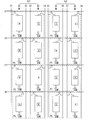
- FIG. 3 is a schematic diagram illustrating a pixel arrangement of the liquid crystal display device of Example 1.
- 1 is a schematic diagram illustrating an overall configuration of a liquid crystal display device of Example 1.
- FIG. It is a schematic diagram which shows the drive method (upper and lower division drive) of Example 1.
- 3 is a schematic diagram illustrating a pixel structure of the liquid crystal display device of Example 1.
- FIG. 5 is a schematic diagram illustrating a driving method of each pixel in FIG. 4.
- FIG. 10 is a schematic diagram illustrating a modification example (with respect to the area of a sub-pixel) of Example 1.
- FIG. 6 is a schematic diagram illustrating a modification example (sub-pixel color) of the first exemplary embodiment.
- FIG. 6 is a schematic diagram illustrating a pixel arrangement of a liquid crystal display device of Example 2.
- FIG. 9 is a schematic diagram illustrating a modification example (sub-pixel color) of the second embodiment.
- FIG. 10 is a schematic diagram illustrating a modified example (sub-pixel color) of the pixel arrangement of the second embodiment.
- 6 is a schematic diagram illustrating a pixel arrangement of a liquid crystal display device of Example 3.
- FIG. 10 is a schematic diagram illustrating a modification example of the pixel arrangement of the third embodiment.
- FIG. 10 is a schematic diagram illustrating a further modification of the pixel arrangement of the third embodiment.
- 6 is a schematic diagram illustrating a pixel arrangement of a liquid crystal display device of Example 4.
- FIG. 9 is a schematic diagram illustrating a modification example (sub-pixel color) of the second embodiment.
- FIG. 10 is a schematic diagram illustrating a modified example (sub-pixel color) of the pixel arrangement of the second embodiment.
- 6 is a schematic diagram
- FIG. 10 is a schematic diagram illustrating a further modification of the pixel array of Embodiment 1.
- FIG. 10 is a schematic diagram illustrating a further modification of the pixel arrangement of the second embodiment.
- FIG. 10 is a schematic diagram illustrating a further modification of the pixel arrangement of the third embodiment. It is a schematic diagram which shows the form which replaced the yellow pixel of FIG. 11 with the white pixel. It is a schematic diagram which shows the modification of FIG. It is a schematic diagram which shows the form which replaced the yellow pixel of FIG. 12 with the white pixel. It is a schematic diagram which shows the form which replaced the yellow pixel of FIG. 13 with the white pixel. It is a schematic diagram which shows the form which replaced the yellow pixel of FIG. 14 with the white pixel.
- Embodiments of the present invention will be described with reference to FIGS. 1 to 22 as follows.
- the liquid crystal display device LCD of Example 1 includes a liquid crystal panel LCP, a display control circuit DCC, first and second source drivers SDA / SDB, and first to fourth gate drivers GDA / GDB.
- a gda / gdb and a backlight BL are provided.
- the liquid crystal panel LCP includes a plurality of data signal lines extending in the column direction (scanning direction), a plurality of scanning signal lines extending in the row direction (lateral direction), and a plurality of pixels arranged in a matrix, and a display unit Is a direct view type with a diagonal of 30 inches or more (1 inch is 0.0254 [m]) or more and a display unit has a resolution of 100 ppi (100 pixels per inch, 10000 pixels in one square) or more.
- the number of pixels in the horizontal direction is larger than 1920 pixels (so-called 2K) of the standard of high-definition television broadcasting, and for example, so-called 4K (4000 pixels) such as 3840 pixels of QFHD and 4096 pixels of DCI are assumed.
- the number of pixels is increasing as the panel size increases, and Super Hi-Vision 8K (7680 pixels) is also targeted.
- the number of pixels in the horizontal direction of the present liquid crystal display device is not limited to the above 2K, 4K, 8K, etc. Of course, 6K, 7K, etc. are also possible.
- the first source driver SDA includes a plurality of driver chips DT arranged in the row direction near the upper end of the panel
- the second source driver SDB includes a plurality of driver chips DT arranged in the row direction near the lower end of the panel. Has been.
- the aspect ratio (horizontal: vertical) of the display unit is generally 16: 9 or 4: 3, but is not limited to this.
- a multi-domain type VA (vertical alignment) mode having high contrast and excellent viewing angle characteristics is desirable. Since the red and blue pixels are arranged sparsely compared to green, color shift occurs in the liquid crystal mode with a narrow viewing angle, and contamination with adjacent pixels in the liquid crystal with low contrast (dirty due to color mixing) It is because it is easy to occur.
- the liquid crystal panel LCP is a so-called vertically divided panel, in which the data signal lines in the first region RA on the upstream side in the scanning direction and the data signal lines in the second region RB on the downstream side in the scanning direction are separated to form the first region RA. And the scanning of the second region RB are performed in parallel.
- the first region RA is scanned by the first and third gate drivers GDA.gda, and the second region RB is scanned by the second and fourth gate drivers GDB.gdb.
- the data signal lines in the first region RA are driven by the first source driver SDA, and the data signal lines in the second region RB are driven by the second source driver SDB.
- the liquid crystal panel LCP is a so-called double source type panel, and, for example, two data signal lines are provided corresponding to one sub-pixel column (SC) of the first region RA. That is, in the liquid crystal display device LCD, as shown in FIG. 3, two scanning signal lines in the first region RA and two scanning signal lines in the second region RB can be simultaneously selected, and high-speed driving is possible. Sometimes the pixel charge rate can be secured.
- the plurality of pixels in the display unit are arranged in the row direction with RG-type pixels including red (R) subpixels SPX and green (G) subpixels SPX arranged in the row direction.
- the pixel is classified into a BG type pixel composed of a blue sub-pixel and a green sub-pixel.
- the RG type and the BG type are alternately arranged every two pixels.
- the RG type and the BG type are alternately arranged for each pixel.
- the R sub-pixel and the G sub-pixel are alternately arranged every two sub-pixels, and in the other (SC), the B sub-pixel and the G sub-pixel are alternately arranged.
- Sub-pixels are alternately arranged every two sub-pixels.
- the pixel P1, the pixel P2, the pixel P5, and the pixel P6 are sequentially arranged in this order in one of the two adjacent pixel columns (PC1), and the pixel P3 and the pixel P4 are arranged in the other (PC2).
- Pixel P7, and pixel P8 are successively arranged in this order, pixel P1 and pixel P3 are adjacent in the row direction, pixel P2 and pixel P4 are adjacent in the row direction, and pixel P5 and pixel P7 are adjacent in the row direction
- the pixel P6 and the pixel P8 are adjacent to each other in the row direction, and in each of the pixels P1 to P8, two subpixels SPX are arranged in the row direction, and each of the pixel P1, the pixel P2, the pixel P7, and the pixel P8 is an RG type.
- Each of the pixel P3, the pixel P4, the pixel P5, and the pixel P6 is a BG type.
- the R subpixel SPX of the pixel P1 and the R subpixel SPX of the pixel P2 are adjacent in the column direction
- the B subpixel SPX of the pixel P5 and the B subpixel SPX of the pixel P6 are adjacent in the column direction.
- the R sub-pixel SPX of the pixel P2 and the B sub-pixel SPX of the pixel P5 are arranged diagonally opposite each other.
- FIG. 4 is a schematic diagram showing the pixel structure of the pixels P1 to P8.
- the pixel column PC1 is as follows (data signal lines S1 to S4 corresponding to the pixel column PC1 are arranged in this order). That is, the pixel electrode corresponding to the R subpixel of the pixel P1 is connected to the data signal line S1 and the scanning signal line G1 via the transistor, and the pixel electrode corresponding to the R subpixel of the pixel P2 is connected to the data via the transistor.
- the pixel electrode connected to the signal line S2 and the scanning signal line G2 and corresponding to the G subpixel of the pixel P5 is connected to the data signal line S1 and the scanning signal line G3 via the transistor, and is connected to the G subpixel of the pixel P6.
- the corresponding pixel electrode is connected to the data signal line S2 and the scanning signal line G4 through transistors.
- the pixel electrode corresponding to the G subpixel of the pixel P1 is connected to the data signal line S4 and the scanning signal line G1 via a transistor, and the pixel electrode corresponding to the G subpixel of the pixel P2 is connected to the data via the transistor.
- the pixel electrode connected to the signal line S3 and the scanning signal line G2 and corresponding to the B subpixel of the pixel P5 is connected to the data signal line S4 and the scanning signal line G3 via the transistor, and is connected to the B subpixel of the pixel P6.
- the corresponding pixel electrode is connected to the data signal line S3 and the scanning signal line G4 through a transistor. Note that a liquid crystal capacitor is formed between the pixel electrode corresponding to each sub-pixel and the common electrode COM.
- FIG. 5 is a schematic diagram showing a driving method of the pixels P1 to P8.
- the pixels P1, P2, P5, and P6 are as follows. That is, when the scanning signal lines G1 and G2 are simultaneously selected (scanned), a positive signal potential is written from the data signal line S1 to the pixel electrode corresponding to the R sub-pixel of the pixel P1, and the G of the pixel P1 A negative signal potential is written from the data signal line S4 to the pixel electrode corresponding to the subpixel, and a negative signal potential is written from the data signal line S2 to the pixel electrode corresponding to the R subpixel of the pixel P2. A positive signal potential is written from the data signal line S3 to the pixel electrode corresponding to the G sub-pixel of P2.
- a positive signal potential is written from the data signal line S1 to the pixel electrode corresponding to the G sub-pixel of the pixel P5, and B of the pixel P5
- a negative signal potential is written from the data signal line S4 to the pixel electrode corresponding to the subpixel
- a negative signal potential is written from the data signal line S2 to the pixel electrode corresponding to the G subpixel of the pixel P6.
- a positive signal potential is written from the data signal line S3 to the pixel electrode corresponding to the B subpixel of P6.
- the display unit is composed of RG type pixels and BG type pixels, but considering that the diagonal of the display unit is 30 inches or more and the normal viewing distance is 1 m or more. If the resolution of the display unit is 100 ppi or more, it is impossible to recognize (distinguish) one pixel with human visual ability. Since each pixel includes G sub-pixels with high human recognition ability, the number of pixels in the row direction (horizontal direction) is substantially reduced without degrading image quality (when one pixel is composed of three color sub-pixels). 2) (compared to the above), the number of driver chips DT can be reduced, and a source driver can be mounted. Accordingly, it is possible to easily realize a liquid crystal display device having a diagonal of 30 inches or more and a resolution of 100 ppi or more.
- the RG type and the BG type are alternately arranged every two pixels in each pixel column, and further, the G sub-pixels are checkered (one grid is for two sub-pixels adjacent in the column direction). Therefore, it is possible to enhance the fineness more than the number of pixels.
- the backlight BL is preferably a direct type including a red LED, a blue LED, and a green LED, and preferably includes a backlight adjustment unit that individually adjusts the luminance of each color.
- the brightness of green which has more pixels than red and blue, is set lower from the viewpoint of white balance.
- the white balance adjustment by the backlight is performed by adjusting the transmittance of the color filter, adjusting the transmittance of the liquid crystal mode (adjustment using different signal voltages for the same gradation), or the thickness of the liquid crystal layer according to the color. It is much easier than adjustment and is an excellent method from the viewpoint of mass productivity.
- R subpixels and G subpixels are alternately arranged every two subpixels, and in the other (SC), B subpixels are arranged alternately.
- the pixels and the G sub-pixels are alternately arranged every two sub-pixels, but the present invention is not limited to this.
- the G subpixel in one of the two adjacent sub pixel columns (SC), only the G sub pixel may be arranged in a straight line.
- the G subpixel can be made smaller than the R and B subpixels.
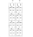
- FIG. 8 is a schematic diagram illustrating a pixel array of the display unit in the second embodiment.
- the size and resolution of the display unit are the same as those in the first embodiment.
- the plurality of pixels in the display unit are arranged in the row direction with RG-type pixels including red (R) subpixels SPX and green (G) subpixels SPX arranged in the row direction.
- the pixel is classified into a BG type pixel composed of a blue subpixel and a green subpixel.
- the RG type and the BG type are alternately arranged for each pixel. Even in the row, the RG type and the BG type are alternately arranged for each pixel.
- the R sub pixel and the G sub pixel are alternately arranged for each sub pixel, and in the other (SC), the B sub pixel and the G sub pixel are alternately arranged.
- Sub-pixels are alternately arranged for each sub-pixel.
- each of the pixel P1, the pixel P4, the pixel P5, and the pixel P8 is an RG type
- each of the pixel P2, the pixel P3, the pixel P6, and the pixel P7 is a BG type.
- the display unit of the second embodiment is also composed of RG type pixels and BG type pixels.
- each pixel includes G subpixels having high human recognition ability, the image quality is hardly deteriorated in the row direction.
- the number of pixels in the (horizontal direction) can be reduced to 2/3 (compared to a case where one pixel is composed of three color sub-pixels), and a source driver can be mounted. Accordingly, it is possible to easily realize a liquid crystal display device having a diagonal of 30 inches or more and a resolution of 100 ppi or more.
- the RG type and the BG type are alternately arranged for each pixel in each pixel column, and further, the G subpixels are checkered (one grid is one subpixel adjacent in the column direction). Therefore, it is possible to enhance the sense of detail.
- the G sub-pixel can be made smaller than the R and B sub-pixels.
- the G sub-pixel in one of the two adjacent subpixel columns (SC), only the G subpixels may be arranged in a straight line. Further, in the configuration of FIG. 10, as shown in FIG. 16, the G sub-pixel can be made smaller than the R and B sub-pixels.
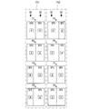
- FIG. 11 is a schematic diagram illustrating a pixel array of a display unit according to the third embodiment.
- the size and resolution of the display unit are the same as those in the first embodiment.
- the plurality of pixels in the display unit are arranged in the row direction with RG-type pixels including red (R) subpixels SPX and green (G) subpixels SPX arranged in the row direction.
- the pixel is classified into a BY (BH) pixel composed of a blue (B) sub-pixel and a yellow (Y) sub-pixel.
- BH BY
- pixel column PC1 or PC2
- RG type and BY type are alternately arranged for each pixel. Further, in one of the two adjacent sub pixel columns (SC), the R sub pixel and the Y sub pixel are alternately arranged every two sub pixels, and in the other (SC), the B sub pixel and the G sub pixel are arranged. Sub-pixels are alternately arranged every two sub-pixels.
- each of the pixel P1, the pixel P2, the pixel P7, and the pixel P8 is an RG type
- each of the pixel P3, the pixel P4, the pixel P5, and the pixel P6 is a BY type.
- the R subpixel SPX of the pixel P1 and the R subpixel SPX of the pixel P2 are adjacent in the column direction
- the B subpixel SPX of the pixel P5 and the B subpixel SPX of the pixel P6 are adjacent in the column direction.
- the R sub-pixel SPX of the pixel P2 and the B sub-pixel SPX of the pixel P5 are arranged diagonally opposite each other.
- the display unit of the third embodiment includes RG type pixels and BY type pixels.
- each pixel includes G or Y sub-pixels having high human recognition ability, the image quality is hardly deteriorated.
- the number of pixels in the row direction (lateral direction) can be reduced to 2/3 (compared to a case where one pixel is composed of three color sub-pixels), and a source driver can be mounted. Accordingly, it is possible to easily realize a liquid crystal display device having a diagonal of 30 inches or more and a resolution of 100 ppi or more.
- each pixel column is alternately arranged with an RG type and a BY type every two pixels in each pixel column, and the Y / G sub-pixels are in a checkered pattern (one grid in the column direction). Therefore, it is possible to enhance the sense of detail.
- yellow has a higher human recognition ability than green
- the sense of detail can be further enhanced by mixing yellow sub-pixels.
- the transmittance is increased and the color purity is increased as compared with the case where yellow is formed by the combination of the R subpixel and the G subpixel, it contributes to low power consumption.
- a higher definition (high resolution) liquid crystal panel can be used if the power consumption is the same.
- the G and Y subpixels may be arranged in a straight line. Also in the configuration of FIG. 12, as shown in FIG. 17, the G and Y subpixels can be made smaller than the R and B subpixels. Further, a configuration in which the Y subpixel in FIG. 12 is replaced with a white (W) subpixel is also possible (see FIG. 20).
- the plurality of pixels of the display unit include an RG type pixel composed of a red (R) sub-pixel SPX and a green (G) sub-pixel SPX arranged in the row direction, and a row direction.
- RY type pixels composed of red (R) sub-pixels SPX and yellow (Y) sub-pixels SPX, and blue (B) sub-pixels and yellow (Y) sub-pixels aligned in the row direction.
- BH type BY type
- BG type pixel composed of a blue (B) sub-pixel and a red (G) sub-pixel arranged in the row direction.
- the RY type is alternately arranged for each pixel.
- the BY type and the BG type are alternately arranged for each pixel.
- G and Y A configuration in which only the sub-pixels are arranged in a straight line is also possible.
- color crosstalk can occur in principle, but according to the inventor's analysis. In natural images (actual images taken with a camera), the correlation between the green and yellow components is very high, so there is little influence of color crosstalk and they can be handled as the same color.
- a configuration in which the Y subpixel in FIG. 13 is replaced with a white (W) subpixel is also possible (see FIG. 21).
- FIG. 14 is a schematic diagram illustrating a pixel array of a display unit according to the fourth embodiment.
- the size and resolution of the display unit are the same as those in the first embodiment.
- the plurality of pixels in the display unit are arranged in the row direction with RG-type pixels including red (R) subpixels SPX and green (G) subpixels SPX arranged in the row direction. It is classified into BY type (BH type) pixels composed of blue subpixels and yellow subpixels.
- RG type and BY type are alternately arranged for each pixel.
- the RG type and the BY type are alternately arranged for each pixel.
- the R sub pixel and the Y sub pixel are alternately arranged for each sub pixel, and in the other (SC), the B sub pixel and the G sub pixel are arranged. Sub-pixels are alternately arranged for each sub-pixel.
- each of the pixel P1, the pixel P4, the pixel P5, and the pixel P8 is an RG type
- each of the pixel P2, the pixel P3, the pixel P6, and the pixel P7 is a BY type.
- the R sub-pixel SPX of the pixel P1 and the B sub-pixel SPX of the pixel P2 pixel are arranged obliquely opposite to each other, and the G sub-pixel SPX of the pixel P1 and the G sub-pixel SPX of the pixel P4 are mutually connected. It is arranged diagonally opposite.
- the display unit of the fourth embodiment is also composed of RG type pixels and BY type pixels.
- each pixel includes Y or G sub-pixels having high human recognition ability, the image quality is hardly deteriorated.
- the number of pixels in the row direction (horizontal direction) can be reduced to 2/3 (compared to a case where one pixel is composed of three color sub-pixels), and a source driver can be mounted. Accordingly, it is possible to easily realize a liquid crystal display device having a diagonal of 30 inches or more and a resolution of 100 ppi or more.
- Example 2 RG type and BY type are alternately arranged for each pixel in each pixel column, and further, G subpixels are in a checkered pattern (one grid is one subpixel adjacent in the column direction). Therefore, it is possible to enhance the sense of detail.
- a configuration in which the Y subpixel in FIG. 14 is replaced with a white (W) subpixel is also possible (see FIG. 22).
- the present invention is not limited to the above-described embodiments, and those obtained by appropriately modifying the above-described embodiments based on common general technical knowledge and those obtained by combining them are also included in the embodiments of the present invention.
- the liquid crystal display device of the present invention is suitable for various liquid crystal displays and liquid crystal televisions, for example.
- LCD Liquid crystal display device LCP Liquid crystal panel DCC Display control circuit P1 to P8 Pixel SPX Sub-pixel PC1, PC2 Pixel row SC Sub-pixel row DT Driver chip SDA / SDB Source driver GDA / GDB / gda / gdb Gate driver BL Backlight
Landscapes
- Physics & Mathematics (AREA)
- Nonlinear Science (AREA)
- Engineering & Computer Science (AREA)
- General Physics & Mathematics (AREA)
- Chemical & Material Sciences (AREA)
- Crystallography & Structural Chemistry (AREA)
- Mathematical Physics (AREA)
- Optics & Photonics (AREA)
- Computer Hardware Design (AREA)
- Theoretical Computer Science (AREA)
- Microelectronics & Electronic Packaging (AREA)
- Geometry (AREA)
- Liquid Crystal (AREA)
- Liquid Crystal Display Device Control (AREA)
- Control Of Indicators Other Than Cathode Ray Tubes (AREA)
Abstract
Un objet de la présente invention consiste à faciliter l'implémentation d'un dispositif d'affichage à cristaux liquides très haute résolution avec une diagonale supérieure ou égale à 30 pouces et une résolution supérieure ou égale à 100 ppi. L'invention concerne un dispositif d'affichage à cristaux liquides à vision directe, comprenant une unité d'affichage dans laquelle une pluralité de pixels est agencée en matrice, et la diagonale de l'unité d'affichage est supérieure ou égale à 30 pouces. La résolution de l'unité d'affichage est supérieure ou égale à 100 pixels par pouce (ppi). Des pixels 1 à 4 sont inclus dans la pluralité de pixels, un des pixels 1 à 4 étant un type RV composé d'un sous-pixel rouge et d'un sous-pixel vert, et un autre des pixels 1 à 4 étant un type BH composé d'un sous-pixel bleu et d'un sous-pixel soit vert, soit jaune, soit blanc.
Priority Applications (1)
| Application Number | Priority Date | Filing Date | Title |
|---|---|---|---|
| US14/400,657 US9726945B2 (en) | 2012-05-17 | 2013-05-16 | Liquid crystal display device |
Applications Claiming Priority (2)
| Application Number | Priority Date | Filing Date | Title |
|---|---|---|---|
| JP2012-113831 | 2012-05-17 | ||
| JP2012113831A JP6195696B2 (ja) | 2012-05-17 | 2012-05-17 | 液晶表示装置 |
Publications (1)
| Publication Number | Publication Date |
|---|---|
| WO2013172400A1 true WO2013172400A1 (fr) | 2013-11-21 |
Family
ID=49583804
Family Applications (1)
| Application Number | Title | Priority Date | Filing Date |
|---|---|---|---|
| PCT/JP2013/063623 Ceased WO2013172400A1 (fr) | 2012-05-17 | 2013-05-16 | Dispositif d'affichage à cristaux liquides |
Country Status (3)
| Country | Link |
|---|---|
| US (1) | US9726945B2 (fr) |
| JP (1) | JP6195696B2 (fr) |
| WO (1) | WO2013172400A1 (fr) |
Cited By (7)
| Publication number | Priority date | Publication date | Assignee | Title |
|---|---|---|---|---|
| CN104267527A (zh) * | 2014-07-31 | 2015-01-07 | 友达光电股份有限公司 | 像素阵列 |
| CN105097865A (zh) * | 2014-04-23 | 2015-11-25 | 上海和辉光电有限公司 | 应用于主动式有机发光二极管amoled显示器的像素排列结构 |
| CN105204206A (zh) * | 2014-06-19 | 2015-12-30 | 联咏科技股份有限公司 | 显示装置及其驱动模块 |
| CN106873277A (zh) * | 2017-04-12 | 2017-06-20 | 武汉华星光电技术有限公司 | Rgbw显示面板 |
| CN106960863A (zh) * | 2017-03-15 | 2017-07-18 | 上海天马有机发光显示技术有限公司 | 显示像素排布结构、显示面板及显示面板的制备方法 |
| JP2017531839A (ja) * | 2014-09-26 | 2017-10-26 | 京東方科技集團股▲ふん▼有限公司Boe Technology Group Co.,Ltd. | 画像の表示方法及び表示装置 |
| US10380928B2 (en) | 2014-06-04 | 2019-08-13 | Novatek Microelectronics Corp. | Display device and driving module thereof |
Families Citing this family (8)
| Publication number | Priority date | Publication date | Assignee | Title |
|---|---|---|---|---|
| CN104062825B (zh) * | 2014-06-30 | 2017-09-01 | 上海天马微电子有限公司 | 阵列基板、显示面板及显示装置 |
| KR102275712B1 (ko) * | 2014-10-31 | 2021-07-09 | 삼성전자주식회사 | 렌더링 방법, 렌더링 장치 및 전자 장치 |
| KR102287821B1 (ko) * | 2015-02-16 | 2021-08-10 | 삼성디스플레이 주식회사 | 유기 발광 디스플레이 장치 및 이를 포함하는 디스플레이 시스템 |
| KR101686236B1 (ko) * | 2016-07-19 | 2016-12-13 | 한석진 | 대칭적 배열을 가진 rgbgr 디스플레이 장치 |
| JP2018189777A (ja) | 2017-05-01 | 2018-11-29 | 株式会社ジャパンディスプレイ | 表示装置 |
| CN108766378B (zh) * | 2018-05-29 | 2019-12-24 | 深圳市华星光电技术有限公司 | 液晶显示面板的白平衡方法及装置 |
| TWI897658B (zh) * | 2024-09-30 | 2025-09-11 | 友達光電股份有限公司 | 顯示面板 |
| CN119207280B (zh) * | 2024-10-25 | 2026-04-28 | 武汉天马微电子有限公司 | 一种显示面板及显示装置 |
Citations (3)
| Publication number | Priority date | Publication date | Assignee | Title |
|---|---|---|---|---|
| WO2006019025A1 (fr) * | 2004-08-19 | 2006-02-23 | Sharp Kabushiki Kaisha | Dispositif d’affichage de couleurs multiprimaires et dispositif d’affichage a cristaux liquides |
| WO2007119288A1 (fr) * | 2006-03-17 | 2007-10-25 | Sharp Kabushiki Kaisha | Dispositif d'affichage à cristaux liquides |
| JP2008152244A (ja) * | 2006-11-22 | 2008-07-03 | Canon Inc | 表示装置 |
Family Cites Families (8)
| Publication number | Priority date | Publication date | Assignee | Title |
|---|---|---|---|---|
| JPS60218627A (ja) * | 1984-04-13 | 1985-11-01 | Sharp Corp | カラ−液晶表示装置 |
| KR100890024B1 (ko) | 2002-09-18 | 2009-03-25 | 삼성전자주식회사 | 액정 표시 장치 |
| KR100951350B1 (ko) * | 2003-04-17 | 2010-04-08 | 삼성전자주식회사 | 액정 표시 장치 |
| US20080106678A1 (en) * | 2006-11-03 | 2008-05-08 | Wintek Corporation | Color filter structure and displaying panel using the same and displaying method thereof |
| US7742128B2 (en) | 2006-11-22 | 2010-06-22 | Canon Kabushiki Kaisha | Hybrid color display apparatus having large pixel and small pixel display modes |
| US20090073099A1 (en) * | 2007-09-14 | 2009-03-19 | Tpo Displays Corp. | Display comprising a plurality of pixels and a device comprising such a display |
| TW200931363A (en) * | 2008-01-10 | 2009-07-16 | Ind Tech Res Inst | Flat display panel |
| KR101634744B1 (ko) * | 2009-12-30 | 2016-07-11 | 삼성디스플레이 주식회사 | 표시 장치 |
-
2012
- 2012-05-17 JP JP2012113831A patent/JP6195696B2/ja not_active Expired - Fee Related
-
2013
- 2013-05-16 WO PCT/JP2013/063623 patent/WO2013172400A1/fr not_active Ceased
- 2013-05-16 US US14/400,657 patent/US9726945B2/en not_active Expired - Fee Related
Patent Citations (3)
| Publication number | Priority date | Publication date | Assignee | Title |
|---|---|---|---|---|
| WO2006019025A1 (fr) * | 2004-08-19 | 2006-02-23 | Sharp Kabushiki Kaisha | Dispositif d’affichage de couleurs multiprimaires et dispositif d’affichage a cristaux liquides |
| WO2007119288A1 (fr) * | 2006-03-17 | 2007-10-25 | Sharp Kabushiki Kaisha | Dispositif d'affichage à cristaux liquides |
| JP2008152244A (ja) * | 2006-11-22 | 2008-07-03 | Canon Inc | 表示装置 |
Cited By (10)
| Publication number | Priority date | Publication date | Assignee | Title |
|---|---|---|---|---|
| CN105097865A (zh) * | 2014-04-23 | 2015-11-25 | 上海和辉光电有限公司 | 应用于主动式有机发光二极管amoled显示器的像素排列结构 |
| US10380928B2 (en) | 2014-06-04 | 2019-08-13 | Novatek Microelectronics Corp. | Display device and driving module thereof |
| CN105204206A (zh) * | 2014-06-19 | 2015-12-30 | 联咏科技股份有限公司 | 显示装置及其驱动模块 |
| CN105204206B (zh) * | 2014-06-19 | 2018-07-13 | 联咏科技股份有限公司 | 显示装置及其驱动模块 |
| CN104267527A (zh) * | 2014-07-31 | 2015-01-07 | 友达光电股份有限公司 | 像素阵列 |
| CN104267527B (zh) * | 2014-07-31 | 2017-06-23 | 友达光电股份有限公司 | 像素阵列 |
| JP2017531839A (ja) * | 2014-09-26 | 2017-10-26 | 京東方科技集團股▲ふん▼有限公司Boe Technology Group Co.,Ltd. | 画像の表示方法及び表示装置 |
| US10467939B2 (en) | 2014-09-26 | 2019-11-05 | Boe Technology Group Co., Ltd. | Method for displaying image and display device |
| CN106960863A (zh) * | 2017-03-15 | 2017-07-18 | 上海天马有机发光显示技术有限公司 | 显示像素排布结构、显示面板及显示面板的制备方法 |
| CN106873277A (zh) * | 2017-04-12 | 2017-06-20 | 武汉华星光电技术有限公司 | Rgbw显示面板 |
Also Published As
| Publication number | Publication date |
|---|---|
| US9726945B2 (en) | 2017-08-08 |
| JP2013242347A (ja) | 2013-12-05 |
| JP6195696B2 (ja) | 2017-09-13 |
| US20150138488A1 (en) | 2015-05-21 |
Similar Documents
| Publication | Publication Date | Title |
|---|---|---|
| JP6195696B2 (ja) | 液晶表示装置 | |
| US9460670B2 (en) | Array substrate, liquid crystal display panel and liquid crystal display device | |
| JP2025069375A (ja) | 画素配列構造、表示パネル及び表示装置 | |
| US8659725B2 (en) | Pixel structure, liquid crystal display panel and transparent liquid crystal display device | |
| US9257081B2 (en) | Two-screen display device | |
| JP5770073B2 (ja) | 表示装置及び電子機器 | |
| JP4578915B2 (ja) | アクティブマトリクス型液晶表示装置およびそれに用いる液晶表示パネル | |
| JP5480970B2 (ja) | 表示パネル及び表示装置 | |
| CN109671405B (zh) | 一种阵列基板、显示面板及其驱动方法 | |
| TWI431606B (zh) | 立體顯示器及其驅動方法 | |
| CN104299557B (zh) | 一种像素结构、显示基板和显示装置 | |
| US8228375B2 (en) | Stereoscopic display device | |
| KR20120049816A (ko) | 표시 장치 | |
| CN103165088B (zh) | 液晶显示设备及其驱动方法 | |
| JP2011209754A5 (fr) | ||
| WO2017202117A1 (fr) | Structure de pixel, substrat matriciel, dispositif d'affichage et procédé de commande d'un dispositif d'affichage | |
| WO2016192367A1 (fr) | Substrat en réseau et appareil d'affichage | |
| TWI398713B (zh) | 陣列基板以及平面顯示裝置 | |
| CN104280960B (zh) | 液晶面板及其驱动方法、液晶显示器 | |
| CN104820312A (zh) | 像素阵列、显示面板和显示装置 | |
| WO2020215375A1 (fr) | Structure de pixel et dispositif d'affichage | |
| US10818251B2 (en) | Display device and method and device of driving the display device | |
| CN104091524B (zh) | 双视显示装置及其驱动方法 | |
| CN101694557B (zh) | 数组基板以及平面显示装置 | |
| KR101026799B1 (ko) | 6색 액정 표시 장치 |
Legal Events
| Date | Code | Title | Description |
|---|---|---|---|
| 121 | Ep: the epo has been informed by wipo that ep was designated in this application |
Ref document number: 13790354 Country of ref document: EP Kind code of ref document: A1 |
|
| WWE | Wipo information: entry into national phase |
Ref document number: 14400657 Country of ref document: US |
|
| NENP | Non-entry into the national phase |
Ref country code: DE |
|
| 122 | Ep: pct application non-entry in european phase |
Ref document number: 13790354 Country of ref document: EP Kind code of ref document: A1 |