WO2013172417A1 - Galette de microcanaux - Google Patents
Galette de microcanaux Download PDFInfo
- Publication number
- WO2013172417A1 WO2013172417A1 PCT/JP2013/063679 JP2013063679W WO2013172417A1 WO 2013172417 A1 WO2013172417 A1 WO 2013172417A1 JP 2013063679 W JP2013063679 W JP 2013063679W WO 2013172417 A1 WO2013172417 A1 WO 2013172417A1
- Authority
- WO
- WIPO (PCT)
- Prior art keywords
- mcp
- clad
- glass
- microchannel plate
- cladding
- Prior art date
- Legal status (The legal status is an assumption and is not a legal conclusion. Google has not performed a legal analysis and makes no representation as to the accuracy of the status listed.)
- Ceased
Links
Images



Classifications
-
- H—ELECTRICITY
- H01—ELECTRIC ELEMENTS
- H01J—ELECTRIC DISCHARGE TUBES OR DISCHARGE LAMPS
- H01J43/00—Secondary-emission tubes; Electron-multiplier tubes
- H01J43/04—Electron multipliers
-
- H—ELECTRICITY
- H01—ELECTRIC ELEMENTS
- H01J—ELECTRIC DISCHARGE TUBES OR DISCHARGE LAMPS
- H01J43/00—Secondary-emission tubes; Electron-multiplier tubes
- H01J43/04—Electron multipliers
- H01J43/06—Electrode arrangements
- H01J43/18—Electrode arrangements using essentially more than one dynode
- H01J43/24—Dynodes having potential gradient along their surfaces
- H01J43/246—Microchannel plates [MCP]
Definitions
- the present invention is a microchannel plate (hereinafter, referred to as a mass spectrometer, a photoelectron spectrometer, an electron microscope, a photomultiplier tube, etc.) including an ion detector. (Referred to as MCP).
- the microchannel plate has a plate-like structure (main body) and is known as an electron multiplier element in which a plurality of channels are regularly arranged.
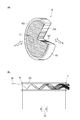
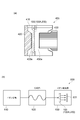
- FIG. 1A is a partially broken view showing a structure of a typical MCP (single clad structure), and FIG. 1B is a diagram for explaining an example of using the MCP.
- the conventional MCP 6 is a thin disk-like structure (main body) mainly composed of lead glass, and a large number of small-diameter holes 62 penetrating in the thickness direction except for the annular outer peripheral portion 61 are disposed. Electrodes 63 are formed on both surfaces of the structure by vapor deposition. The electrode 63 does not cover the entire surface of the MCP 6, but is formed by exposing the outer peripheral portion 61 of the MCP 6 from 0.5 mm to 1.0 mm from the outer peripheral end.
- the MCP 6 has an input side electrode 4 (electrode 63) and an output side electrode 7 (electrode 63) arranged on the front side and the back side, respectively.
- an input side electrode 4 electrode 63
- an output side electrode 7 electrode 63
- MCPs having the above-described structure have been increasingly demanded to expand the dynamic range due to the expansion of the field of use.
- MCP microchannel plate
- MCP is an electron multiplier made of lead glass, and has conductivity by hopping conduction like a semiconductor. Therefore, it is known that the MCP has a temperature characteristic of negative electrical resistance, and the MCP itself generates heat due to the conduction current and the resistance is lowered. In particular, in the case of a low resistance MCP, the phenomenon appears remarkably. Eventually, a thermal runaway may occur, causing the MCP itself to rise to the glass melting temperature (deformation point), or generating a large amount of gas from the glass due to heat generation in the middle of the MCP itself, resulting in a discharge. is there.
- the MCP resistance In order to improve the temperature characteristics of the MCP resistance as described above, it is considered effective to increase the ratio of lead in the glass, which is the main constituent material of the MCP. However, increasing the lead content in the glass greatly reduces the acid resistance of the MCP. In the MCP manufacturing process, since channels (a plurality of holes provided in the glass structure) are formed by etching, it becomes difficult to manufacture the MCP itself, and stable MCP cannot be produced. Moreover, the completed MCP also absorbs moisture in the atmosphere due to the influence of lead depending on the environment (oxidation). In this case, the MCP causes volume expansion, warping and warping, and a possibility of finally reaching a crack.
- the conventional MCP is a structure made of lead glass, the lead glass is exposed to the atmosphere during transportation and storage.
- MCPs with increased lead content and improved dynamic range characteristics have the problem of poor resistance to the environment, such as deterioration of characteristics and changes in shape due to the influence of humidity due to poor acid resistance and strength.
- the present invention has been made to solve the above-described problems, and realizes an MCP having a wider dynamic range and superior environmental resistance (including weather resistance) compared to the prior art and It aims at providing the applied apparatus.
- the microchannel plate (MCP) according to the present invention is a sensing device made of lead glass that exhibits electrical conductivity before the reduction treatment and exhibits conductivity after the reduction treatment.
- the MCP employs a double clad structure composed of two types of clad glasses having different chemical characteristics.
- the MCP includes a plurality of first cladding glasses each having a predetermined resistivity, and a second cladding glass having a resistivity lower than that of the first cladding glass.
- Each of the plurality of first clad glasses has a hollow structure extending along a predetermined direction, and the inner wall surface functions as a channel wall (secondary electron emission layer).
- the second clad glass is a member that fills the gaps between the plurality of first clad glasses that are spaced apart from each other by a predetermined distance. Therefore, at least a part of the second clad glass is located in a space sandwiched between the outer peripheral surfaces of the plurality of first clad glasses in a state of being in contact with the outer peripheral surfaces of the plurality of first clad glasses.
- the resistivity of the first clad glass is made higher than the resistivity of the second clad glass, thereby causing damage due to thermal runaway and degradation of environmental resistance (due to the external environment). Damage due to structural deterioration such as warping is suppressed.
- the dynamic range can be expanded by increasing the strip current.
- each of the resistivity of the first and second clad glasses tends to decrease as the temperature rises. Furthermore, in the above temperature range, the change rate of the resistivity in the first cladding glass is larger than the change rate of the resistivity in the second cladding glass.
- the lead content of the second cladding glass is higher than the lead content of the first cladding glass.
- the fourth aspect applicable to at least one of the first to third aspects is preferable. That is, as a fourth aspect, the first cladding glass before the reduction treatment contains lead oxide in a weight ratio of 20.0% or more and less than 48.0%, and the second cladding glass before the reduction treatment is a weight ratio. It is preferable to contain 48.0% or more and less than 65.0% lead oxide. Furthermore, as a fifth aspect applicable to at least one of the first to fourth aspects, the first clad glass before the reduction treatment has a weight ratio of 40.0% or more and less than 65.0%. It is preferable that the second clad glass containing silicon before the reduction treatment contains silicon dioxide having a weight ratio of 20.0% or more and less than 40.0%.
- the first clad glass may contain zirconium (zirconium oxide before the reduction treatment).
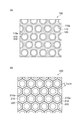
- the second clad glass functions as a main conductive part. Therefore, in order to make the conductivity uniform, it is preferable that the width of the second cladding glass is constant. Therefore, as a seventh aspect applicable to at least one of the first to sixth aspects, in the cross section of the main body perpendicular to the predetermined direction, the outer periphery of the first cladding glass is transformed into a hexagon, The second cladding glass preferably constitutes a honeycomb structure.
- the width of the second clad glass sandwiched between the first clad glass is uniform (a part of the second clad glass sandwiched between the first clad glass has a strip shape having a uniform width) Unevenness in charge supply supplied to the first cladding glass can be effectively suppressed.
- the area ratio of the first cladding glass in the cross section is the second ratio in the cross section. It is smaller than the area ratio of the clad glass. More specifically, as a ninth aspect applicable to at least one of the first to eighth aspects, the area ratio of the second clad glass in the cross section of the main body perpendicular to the predetermined direction is 25% or more is preferable.
- the cross section of the main body is defined only by a glass region that does not include a region corresponding to the space defined by the inner wall of the first cladding glass.
- the MCP (MCP according to the present invention) configured by at least one of the first to ninth aspects as described above, or a combination of these aspects, can be applied to various sensing devices.
- an MCP configured by at least one of the first to ninth aspects or a combination of these aspects can be applied to an image intensifier.
- an MCP configured by a combination of these aspects can be applied to an ion detector.
- the ion detector according to the eleventh aspect can be applied to various inspection apparatuses.
- an inspection apparatus to which the ion detector according to the eleventh aspect is applied includes, for example, a mass spectrometer, a photoelectron spectrometer, An electron microscope or photomultiplier tube is included.
- a mass spectrometer includes an ionization unit that ionizes a sample to be measured, an analysis unit that separates a sample ionized by the ionization unit according to a mass-to-charge ratio, and an ion detection unit that detects ions that have passed through the analysis unit.
- the ion detector includes an MCP configured by at least one of the first to ninth aspects or a combination of these aspects as the ion detector according to the eleventh aspect.
- an MCP that has a wider dynamic range and has superior environmental resistance (including weather resistance) and its application device as compared with the prior art.
- FIG. 4 is a diagram for explaining the structure of a typical MCP
- (a) is a partially broken view showing the structure of a typical MCP (single clad structure)
- (b) is a diagram of the MCP. It is a figure for demonstrating a usage example. These are the figures for demonstrating the structure of the channel vicinity of MCP which concerns on this embodiment. These are figures which show the planar structure of MCP which concerns on a part of MCP (area
- FIG. 10 is a diagram for explaining the structure of the MCP before and after channel formation
- FIG. 10 (a) is a partially cutaway view (FIG. 1 (FIG. 1)) showing the cross-sectional structure of the MCP 28 before channel formation shown in FIG.
- FIG. 1 (b) is a partially broken view of the MCP 28A in which a channel is formed (corresponding to the partially broken view shown in FIG. 1 (a)). is there.
- FIG. 1 (a) is a figure which shows the cross-section of the image intensifier which can apply MCP which concerns on this embodiment
- (b) is this figure It is a conceptual diagram which shows the structure of a mass spectrometer as a test
- MCP microchannel plate
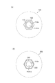
- FIG. 2 is a diagram for explaining the structure in the vicinity of the MCP channel according to the present embodiment.
- FIG. 3 shows a planar structure of the MCP according to the present embodiment corresponding to a part of the MCP (a region indicated by the arrow C) as viewed from the direction indicated by the arrow A in FIG. FIG.
- the MCP according to the present embodiment is an electron multiplier element including a main body made of lead glass that exhibits electrical conductivity before the reduction treatment and exhibits conductivity after the reduction treatment.
- the basic structure of the MCP is shown in FIG. It is similar to the structure of MCP6 shown in a) and FIG. However, the MCP according to the present embodiment is different from the MCP 6 shown in FIGS. 1A and 1B in the structure of the main body (structure) in which a plurality of holes each defining a channel are formed. . That is, the MCP 6 structure has a single clad structure, whereas the MCP main body according to the present embodiment has a double clad structure.
- the MCP 100 according to the present embodiment shown in FIG. 2A is directly provided on the first cladding 110 (first cladding glass) whose inner wall 110 a functions as a channel wall and on the outer peripheral surface of the first cladding 110.
- the second clad 120 (second clad glass) is provided.
- the double clad structure shown in FIG. 2A is two-dimensionally arranged.
- the MCP 200 according to the present embodiment shown in FIG. 2B has a first clad 210 (first clad glass) whose inner wall 210 a functions as a channel wall and directly on the outer peripheral surface of the first clad 210.
- a second clad 220 (second clad glass) is provided.
- the double clad structure shown in FIG. 2B is two-dimensionally arranged.
- the outer periphery of the first cladding 210 is deformed into a hexagonal shape, so that the second cladding 220 forms a honeycomb structure.
- the lead content of the second clad 120 and 220 is larger than the lead content of the first clad 110 and 210. It has become. Due to the adjustment of the lead content, the resistivity of the second cladding 120 and 220 is lower than the resistivity of the first cladding 110 and 210. Further, in the comparison before the reduction treatment, the acid resistance of the first cladding 110 and 210 is higher than the acid resistance of the second cladding 120 and 220.
- Each acid resistance of the first cladding 110 and 210 and the second cladding 120 and 220 means resistance to any one of hydrochloric acid, nitric acid, sulfuric acid, phosphoric acid, or a mixed solution thereof.
- the weight ratio of silicon dioxide (SiO 2 ) is 40.0% or more and less than 65.0% as the composition of the first claddings 110 and 210 by experiments described later.
- the weight ratio of PbO) is preferably 20.0% or more and less than 48.0%.
- zirconium oxide is contained before the reduction treatment in order to improve the acid resistance of the first claddings 110 and 210.
- the weight ratio of silicon dioxide (SiO 2 ) is preferably 20.0% or more and less than 40.0%, and the weight ratio of lead oxide (PbO) before the reduction treatment. Is preferably 48.0% or more and less than 65.0%.
- the specifications of the prototyped MCP are as follows. That is, the outer diameter of the MCP is 25 mm, of which the outer diameter of the MCP effective surface is 20 mm.
- the bias angle is 8 degrees.
- the resistance of the entire MCP was 2.2 M ⁇ , and the gain was 16000 per 1 kV.
- the resistance of the MCP prototyped using only the first cladding 110 and 210 was 54.0 M ⁇ , and the gain was 17000 per 1 kV.
- the resistance of the MCP prototyped using only the second cladding 120 and 220 was 1.0 M ⁇ , and the gain was 21000 per 1 kV.
- the design resistance value of the entire MCP can be changed by changing the area ratio (or volume ratio) of each cladding. Further, it is possible to reduce the resistance value of the entire MCP by increasing the lead content of the second claddings 120 and 220.
- FIG. 5 the structure of the MCPs 100 and 200 adopting the double clad structure is described, but in the present embodiment, as illustrated in FIG. 5.
- a structure may be employed. That is, in the MCP 100A of FIG. 5, a high acid-resistant coating material 300 replaces the first clad 110 in the MCP 100 shown in FIG. 2A, and the holes for defining the channels provided in the second clad 120. It is provided on the inner wall. Therefore, in the MCP 100A, the inner wall 300a of the coating material 300 having high acid resistance functions as a channel wall.
- the coating material 300 an Al 2 O 3 film formed with a desired film thickness by an atomic layer deposition method (ALD) can be given.
- ALD atomic layer deposition method
- FIG. 4 is a plan view showing an example of the cross-sectional structure of the MCP according to the present embodiment, which corresponds to the cross-section of the MCP viewed from the direction indicated by the arrow B in FIG.
- FIG. 5 is a plan view showing another example of the cross-sectional structure of the MCP according to the present embodiment, corresponding to the cross-section of the MCP viewed from the direction indicated by the arrow B in FIG.
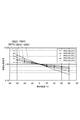
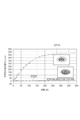
- FIG. 6 is a graph showing the relationship between the normalized resistivity ( ⁇ ⁇ m) and the operating temperature (° C.) (resistivity change rate) for various samples 1 to 5 of the single clad MCP.
- Table 1 shows the resistivity of Samples 1 to 5 in each of a plurality of temperature environments
- Table 2 is a table corresponding to FIG. 6 and is a sample based on the resistivity at a temperature of 0 degrees.
- a normalized resistivity of 1 to 5 is shown.
- FIG. 7 is a graph showing the environmental resistance of samples with different lead oxide contents of a single clad MCP in relation to the relative change in days and flatness.
- graph G610 shows the environmental resistance (standardized resistivity shown in Table 2) of a single clad MCP (Sample 1) having a PbO content of 28.0% before the reduction treatment.
- graph G620 shows the environmental resistance of a single clad MCP (sample 2) having a PbO content of 35.0% before the reduction treatment
- graph G630 shows a PbO content of 43.0% before the reduction treatment.
- graph G640 shows environmental resistance of single clad MCP (sample 4) having a PbO content of 50.5% before reduction treatment
- graph G650 shows PbO before reduction treatment
- Each shows the environmental resistance of a single clad MCP (Sample 5) with a content of 54.5%.
- G710 shows the environmental resistance (flatness change) of the single clad MCP having a PbO content of 51.0% before the reduction treatment
- the graph G720 shows a PbO content of 43% as a comparative example. It shows the environmental resistance of a single clad MCP. As shown in FIG. 7, the environmental resistance deteriorates significantly when the amount of lead oxide is large. If left in the air, the MCP itself will be damaged, and structural deterioration such as cracking will occur.
- FIG. 8 is a graph showing the environmental resistance of various samples of the double clad MCP based on a typical single clad MCP in terms of the number of days and warpage.
- the first cladding 110, 210 is lead oxide having a weight ratio of 20.0% or more and less than 48.0% before the reduction treatment, and the dioxide dioxide having a weight ratio of 40.0% or more and less than 65.0% before the reduction treatment.
- the second clad 120, 220 is lead oxide having a weight ratio of 48.0% or more and less than 65.0% before the reduction treatment, and a dioxide dioxide having a weight ratio of 20.0% or more and less than 40.0% before the reduction treatment. Contains silicon.
- any sample of the double clad MCP can obtain (improved) the same level of environmental resistance as that of the reference single clad MCP.
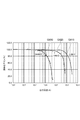
- FIG. 9 is a graph showing saturation characteristics for samples having different MCP structures.
- a graph G910 shows the linearity of the double clad MCP when the MCP resistance is 2.5 M ⁇
- a graph G920 shows the linearity of the single clad MCP when the MCP resistance is 14.0 M ⁇
- a graph G930 shows the MCP.
- the linearity of the single clad MCP when the resistance is 344.0 M ⁇ is shown respectively. Also from this result, it can be seen that even in MCPs having a double clad structure, linearity has been extended by lowering resistance (expansion of dynamic range).
- the inner walls function as channel walls by applying a glass material having excellent acid resistance to the first claddings 110 and 210 (the inner walls function as channel walls), a low resistance MCP having good environmental resistance can be easily manufactured.
- the width of the second clad 220 serving as a main conductive portion becomes constant.
- the deformation points of the first cladding 110, 210 and the second cladding 120, 220 Is preferably the same or close.
- FIGS. 10 (a) to 10 (i) are diagrams for explaining a method of manufacturing the double clad MCP according to the present embodiment.
- FIG. 11 is a diagram for explaining another method for forming channel fibers different from the forming method shown in FIG.
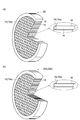
- FIG. 12A is a partially cutaway view (corresponding to the partially cutaway view shown in FIG. 1A) showing the cross-sectional structure of the MCP 28 before the channel formation shown in FIG. 10G.
- FIG. 12B is a partially cutaway view (corresponding to the partially cutaway view shown in FIG. 1B) of the MCP 28A in which the channel is formed.
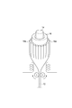
- FIG. 10A is a diagram illustrating a method of forming a channel fiber (first fiber) 12 that can form a channel by a core removal process.
- the channel fiber 12 includes a core portion (center portion) 14 formed of a first glass material having solubility with respect to an acid, and a cladding portion (with a second glass material having insolubility with respect to the same acid) ( The outer peripheral part) 16 was inserted into the tube, and the tube was drawn while heating them.
- a clad portion 18 made of a third glass material that is insoluble in the same acid is further formed on the outer periphery of the clad portion 16.
- the clad portion 18 may be a tube that can accommodate the clad portion 16 therein, or may be a number of glass rods 18a surrounding the clad portion 16 as shown in FIG.
- the clad portion 16 of the channel fiber 12 corresponds to the first clad 210 of the finally obtained MCP 200, and the clad portion 18 or the many glass rods 18 a correspond to the second clad 220.
- the channel fibers 12 are stacked in parallel and closely in a predetermined pattern and aligned in a mold 20 having a regular hexagonal hollow cross section. Thereafter, the channel fibers 12 aligned in the mold 20 are heat-fused and cooled, and then the mold 20 is removed. Thereby, the MF base material 22 having a regular hexagonal cross section is obtained.
- FIG. 10C while the MF base material 22 is heated, the tube is drawn again to make MF10. At that time, the tube is drawn so that the cross section of the MF 10 becomes a regular hexagon. Further, the MF obtained in this step may be stacked in a mold, aligned, and piped to form MF10. Further, this step may be repeated until a desired channel diameter is obtained.
- a plurality of obtained MFs 10 are aligned inside the glass tube 24.
- FIG. 10E is a diagram showing a cross-sectional structure of the MCP plate material 28.
- the core portion 14 remains at a position to be a channel.
- the MCP plate material 28 is dipped in an acid solution, and a centering process is performed.
- the core portion 14 of the channel fiber 12 is eluted because it is formed of the first glass material that is soluble in acid.
- the clad part 16 and the clad part 18 are formed of the second glass material and the third glass material which are insoluble in acid, they do not elute.
- the channel 6 is formed by the elution of the core portion 14.
- a secondary electron emission layer mainly composed of SiO2 is formed on the surface of the channel 6.
- the reduction process is performed by putting the MCP plate material 28A subjected to the core removal process into an electric furnace in a hydrogen atmosphere and heating (see FIG. 10 (i)). Thereby, PbO on the channel surface (inside the secondary electron emission layer) of the MCP plate material 28A is reduced to Pb, and a desired conductive thin film is formed. Also in this case, since the inner diameter of the channel is the same in the corner region and its peripheral region, a homogeneous conductive thin film is formed. Finally, electrode metal is vapor-deposited (not shown) on both sides of the MCP plate 28A, and the MCP 200 is obtained.
- FIG. 13A is a diagram illustrating a cross-sectional structure of an image intensifier to which the MCP according to the present embodiment is applicable.
- the image intensifier 400 includes a ceramic vacuum vessel 410, an incident surface plate 420 installed at one opening end of the vacuum vessel 410, and the other of the vacuum vessel 410.
- a fiber optic plate (FOP) 430 installed at the open end, and an MCP 100 (100A, 200) disposed between the entrance face plate 420 and the FOP 430 are provided.
- FOP fiber optic plate
- a photoelectric surface 420 a that converts light into electrons is formed inside the incident surface plate 420 (inside the vacuum vessel 410), and a fluorescent screen 430 a is formed on the incident surface of the FOP 430.
- the image intensifier 400 is designed to obtain an image without distortion in the peripheral portion by bringing the MCP 100 (100A, 200) and the fluorescent screen 430a that converts electrons into light close to each other.
- the MCP according to the present embodiment can be applied to inspection apparatuses such as a mass spectrometer, a photoelectron spectrometer, an electron microscope, and a photomultiplier tube in addition to the above-described image intensifier (FIG. 13A). It is.
- FIG. 13B shows a conceptual diagram showing the configuration of the mass spectrometer.
- the mass spectrometer 500 includes an ionization unit 510 that ionizes a measurement target sample, an analysis unit 520 that separates the ionized sample according to a mass-to-charge ratio, and an analysis unit 520. It is comprised by the ion detection part 530 which detects the ion which passed.
- the ion detection unit 530 includes the MCP according to the present embodiment and an anode 531.
- any of the MCPs 100, 100A, and 200 according to the present embodiment functions as an electron multiplier that emits secondary electrons in response to incident ions.
- the anode 531 takes out secondary electrons emitted from the MCP as a signal.
- conventional MCPs have been limited in terms of manufacturing and characteristics due to problems of acid resistance and strength because they have been made low resistance MCPs by increasing the lead content in order to expand the dynamic range.
- the low resistance MCP can be easily manufactured, and the MCP characteristics can be stabilized.
- TOF-MS Time FlightMCMass Spectrometer
- MCP structural degradation
Landscapes
- Electron Tubes For Measurement (AREA)
- Image-Pickup Tubes, Image-Amplification Tubes, And Storage Tubes (AREA)
Priority Applications (2)
| Application Number | Priority Date | Filing Date | Title |
|---|---|---|---|
| JP2014515672A JP6211515B2 (ja) | 2012-05-18 | 2013-05-16 | マイクロチャネルプレート、イメージインテンシファイヤ、荷電粒子検出器および検査装置 |
| EP13791653.2A EP2851932B1 (fr) | 2012-05-18 | 2013-05-16 | Galette de microcanaux |
Applications Claiming Priority (2)
| Application Number | Priority Date | Filing Date | Title |
|---|---|---|---|
| US201261648756P | 2012-05-18 | 2012-05-18 | |
| US61/648756 | 2012-05-18 |
Publications (1)
| Publication Number | Publication Date |
|---|---|
| WO2013172417A1 true WO2013172417A1 (fr) | 2013-11-21 |
Family
ID=49580547
Family Applications (1)
| Application Number | Title | Priority Date | Filing Date |
|---|---|---|---|
| PCT/JP2013/063679 Ceased WO2013172417A1 (fr) | 2012-05-18 | 2013-05-16 | Galette de microcanaux |
Country Status (4)
| Country | Link |
|---|---|
| US (1) | US9117640B2 (fr) |
| EP (1) | EP2851932B1 (fr) |
| JP (1) | JP6211515B2 (fr) |
| WO (1) | WO2013172417A1 (fr) |
Cited By (2)
| Publication number | Priority date | Publication date | Assignee | Title |
|---|---|---|---|---|
| WO2019003567A1 (fr) * | 2017-06-30 | 2019-01-03 | 浜松ホトニクス株式会社 | Multiplicateur d'électrons |
| WO2019003568A1 (fr) * | 2017-06-30 | 2019-01-03 | 浜松ホトニクス株式会社 | Multiplicateur d'électrons |
Families Citing this family (4)
| Publication number | Priority date | Publication date | Assignee | Title |
|---|---|---|---|---|
| GB2475063A (en) * | 2009-11-04 | 2011-05-11 | Univ Leicester | Charge detector for photons or particles. |
| EP2851931B1 (fr) * | 2012-05-18 | 2017-12-13 | Hamamatsu Photonics K.K. | Galette de microcanaux |
| EP2851932B1 (fr) | 2012-05-18 | 2017-12-20 | Hamamatsu Photonics K.K. | Galette de microcanaux |
| JP6340102B1 (ja) * | 2017-03-01 | 2018-06-06 | 浜松ホトニクス株式会社 | マイクロチャンネルプレート及び電子増倍体 |
Citations (6)
| Publication number | Priority date | Publication date | Assignee | Title |
|---|---|---|---|---|
| JPS63128544A (ja) * | 1986-11-03 | 1988-06-01 | リトン システムズ,インコーポレーテツド | マイクロチヤネルプレート |
| JPS6417351A (en) * | 1987-07-10 | 1989-01-20 | Matsushita Electric Industrial Co Ltd | Manufacture of secondary electron multiplier |
| JPH0210645A (ja) * | 1988-03-24 | 1990-01-16 | Galileo Electro Opt Corp | チャンネル電子増倍器 |
| WO2006123447A1 (fr) * | 2005-05-17 | 2006-11-23 | Kyoto University | Dispositif d'exposition d'un faisceau d'electrons |
| JP2011513921A (ja) * | 2008-02-27 | 2011-04-28 | アラディアンス インコーポレイテッド | 複数の放出層を有するマイクロチャネルプレートデバイス |
| JP2011129362A (ja) * | 2009-12-17 | 2011-06-30 | Institute Of Physical & Chemical Research | マイクロチャネルプレート組立体及びマイクロチャネルプレート検出器 |
Family Cites Families (23)
| Publication number | Priority date | Publication date | Assignee | Title |
|---|---|---|---|---|
| US3979621A (en) | 1969-06-04 | 1976-09-07 | American Optical Corporation | Microchannel plates |
| US3673457A (en) * | 1969-11-25 | 1972-06-27 | Corning Glass Works | High gain storage target |
| US3979637A (en) | 1971-11-08 | 1976-09-07 | American Optical Corporation | Microchannel plates and method of making same |
| JPS53107267A (en) | 1977-03-02 | 1978-09-19 | Hamamatsu Tv Co Ltd | Method of producing channel plate |
| DE3317778A1 (de) | 1982-05-17 | 1983-11-17 | Galileo Electro-Optics Corp., Sturbridge, Mass. | Glas |
| JPS61140044A (ja) | 1984-12-11 | 1986-06-27 | Hamamatsu Photonics Kk | マイクロチヤンネルプレ−トの製造方法 |
| US4912314A (en) * | 1985-09-30 | 1990-03-27 | Itt Corporation | Channel type electron multiplier with support rod structure |
| US4983551A (en) * | 1988-08-13 | 1991-01-08 | Galileo Electro-Optics Corp. | Channel electron multipliers |
| US5034354A (en) | 1990-05-16 | 1991-07-23 | Corning Incorporated | Alkali-free multichannel plate and glass |
| US5493169A (en) * | 1994-07-28 | 1996-02-20 | Litton Systems, Inc. | Microchannel plates having both improved gain and signal-to-noise ratio and methods of their manufacture |
| US6040000A (en) | 1998-03-24 | 2000-03-21 | Itt Manufacturing Enterprises, Inc. | Method and apparatus for a microchannel plate having a fissured coating |
| JP2001351509A (ja) * | 2000-06-08 | 2001-12-21 | Hamamatsu Photonics Kk | マイクロチャネルプレート |
| JP2002033068A (ja) * | 2000-07-14 | 2002-01-31 | Nikon Corp | 荷電粒子ビーム欠陥検査装置及び方法 |
| US6917144B2 (en) * | 2002-08-16 | 2005-07-12 | Litton Systems, Inc. | Microchannel plate having input/output face funneling |
| WO2004112072A2 (fr) | 2003-05-29 | 2004-12-23 | Nova Scientific, Inc. | Multiplicateur d'electrons et detecteur de rayonnement |
| US7221837B2 (en) * | 2003-06-20 | 2007-05-22 | Itt Manufacturing Enterprises, Inc. | Device and method for reducing glass flow during the manufacture of microchannel plates |
| US7081618B2 (en) * | 2004-03-24 | 2006-07-25 | Burle Technologies, Inc. | Use of conductive glass tubes to create electric fields in ion mobility spectrometers |
| US8052884B2 (en) * | 2008-02-27 | 2011-11-08 | Arradiance, Inc. | Method of fabricating microchannel plate devices with multiple emissive layers |
| EP2274762B1 (fr) * | 2008-04-10 | 2018-06-06 | Arradiance, LLC | Dispositif d'intensification d'image |
| US8227965B2 (en) * | 2008-06-20 | 2012-07-24 | Arradiance, Inc. | Microchannel plate devices with tunable resistive films |
| US8237129B2 (en) | 2008-06-20 | 2012-08-07 | Arradiance, Inc. | Microchannel plate devices with tunable resistive films |
| EP2851932B1 (fr) | 2012-05-18 | 2017-12-20 | Hamamatsu Photonics K.K. | Galette de microcanaux |
| WO2013172278A1 (fr) | 2012-05-18 | 2013-11-21 | 浜松ホトニクス株式会社 | Plaque à microcanaux |
-
2013
- 2013-05-16 EP EP13791653.2A patent/EP2851932B1/fr not_active Not-in-force
- 2013-05-16 WO PCT/JP2013/063679 patent/WO2013172417A1/fr not_active Ceased
- 2013-05-16 US US13/895,534 patent/US9117640B2/en active Active
- 2013-05-16 JP JP2014515672A patent/JP6211515B2/ja not_active Expired - Fee Related
Patent Citations (6)
| Publication number | Priority date | Publication date | Assignee | Title |
|---|---|---|---|---|
| JPS63128544A (ja) * | 1986-11-03 | 1988-06-01 | リトン システムズ,インコーポレーテツド | マイクロチヤネルプレート |
| JPS6417351A (en) * | 1987-07-10 | 1989-01-20 | Matsushita Electric Industrial Co Ltd | Manufacture of secondary electron multiplier |
| JPH0210645A (ja) * | 1988-03-24 | 1990-01-16 | Galileo Electro Opt Corp | チャンネル電子増倍器 |
| WO2006123447A1 (fr) * | 2005-05-17 | 2006-11-23 | Kyoto University | Dispositif d'exposition d'un faisceau d'electrons |
| JP2011513921A (ja) * | 2008-02-27 | 2011-04-28 | アラディアンス インコーポレイテッド | 複数の放出層を有するマイクロチャネルプレートデバイス |
| JP2011129362A (ja) * | 2009-12-17 | 2011-06-30 | Institute Of Physical & Chemical Research | マイクロチャネルプレート組立体及びマイクロチャネルプレート検出器 |
Non-Patent Citations (1)
| Title |
|---|
| See also references of EP2851932A4 * |
Cited By (6)
| Publication number | Priority date | Publication date | Assignee | Title |
|---|---|---|---|---|
| WO2019003567A1 (fr) * | 2017-06-30 | 2019-01-03 | 浜松ホトニクス株式会社 | Multiplicateur d'électrons |
| WO2019003568A1 (fr) * | 2017-06-30 | 2019-01-03 | 浜松ホトニクス株式会社 | Multiplicateur d'électrons |
| JP2019012658A (ja) * | 2017-06-30 | 2019-01-24 | 浜松ホトニクス株式会社 | 電子増倍体 |
| JP2019012659A (ja) * | 2017-06-30 | 2019-01-24 | 浜松ホトニクス株式会社 | 電子増倍体 |
| US11011358B2 (en) | 2017-06-30 | 2021-05-18 | Hamamatsu Photonics K.K. | Electron multiplier having resistance value variation suppression and stablization |
| US11170983B2 (en) | 2017-06-30 | 2021-11-09 | Hamamatsu Photonics K.K. | Electron multiplier that suppresses and stabilizes a variation of a resistance value in a wide temperature range |
Also Published As
| Publication number | Publication date |
|---|---|
| EP2851932A4 (fr) | 2016-03-16 |
| JPWO2013172417A1 (ja) | 2016-01-12 |
| EP2851932B1 (fr) | 2017-12-20 |
| EP2851932A1 (fr) | 2015-03-25 |
| US20130306852A1 (en) | 2013-11-21 |
| JP6211515B2 (ja) | 2017-10-11 |
| US9117640B2 (en) | 2015-08-25 |
Similar Documents
| Publication | Publication Date | Title |
|---|---|---|
| JP6340119B2 (ja) | マイクロチャネルプレートの製造方法 | |
| JP6211515B2 (ja) | マイクロチャネルプレート、イメージインテンシファイヤ、荷電粒子検出器および検査装置 | |
| JP6220780B2 (ja) | マイクロチャネルプレート、イメージインテンシファイヤ、荷電粒子検出器および検査装置 | |
| US10522316B2 (en) | X-ray source | |
| US8052884B2 (en) | Method of fabricating microchannel plate devices with multiple emissive layers | |
| JP6097201B2 (ja) | イオン移動の障壁を有するマイクロチャネルプレートの製造方法 | |
| US20040005433A1 (en) | Micro-channel plate | |
| KR20130114137A (ko) | 나노 다이아몬드층을 가지는 전자 증배기 장치 | |
| US20140028175A1 (en) | Microchannel Plate Devices With Tunable Resistive Films | |
| US10340129B2 (en) | Microchannel plate and electron multiplier | |
| US8710455B2 (en) | Charged-particle beam lens | |
| JP5161295B2 (ja) | 電界放出装置及びその製造方法 | |
| JP5956292B2 (ja) | 電子管 | |
| Cremer et al. | Recent developments in next-generation microchannel plates for particle identification applications | |
| Xie et al. | Fast-timing microchannel plate photodetectors: Design, fabrication, and characterization | |
| US20110287684A1 (en) | Method for making field emission device | |
| KR20070046617A (ko) | 절연체층, 이를 포함한 전자 방출 소자 및 전자 방출디스플레이 장치 |
Legal Events
| Date | Code | Title | Description |
|---|---|---|---|
| 121 | Ep: the epo has been informed by wipo that ep was designated in this application |
Ref document number: 13791653 Country of ref document: EP Kind code of ref document: A1 |
|
| ENP | Entry into the national phase |
Ref document number: 2014515672 Country of ref document: JP Kind code of ref document: A |
|
| WWE | Wipo information: entry into national phase |
Ref document number: 2013791653 Country of ref document: EP |
|
| NENP | Non-entry into the national phase |
Ref country code: DE |