WO2013175681A1 - Récepteur à conversion directe - Google Patents
Récepteur à conversion directe Download PDFInfo
- Publication number
- WO2013175681A1 WO2013175681A1 PCT/JP2013/001408 JP2013001408W WO2013175681A1 WO 2013175681 A1 WO2013175681 A1 WO 2013175681A1 JP 2013001408 W JP2013001408 W JP 2013001408W WO 2013175681 A1 WO2013175681 A1 WO 2013175681A1
- Authority
- WO
- WIPO (PCT)
- Prior art keywords
- frequency converter
- signal
- receiver
- voltage
- unit
- Prior art date
- Legal status (The legal status is an assumption and is not a legal conclusion. Google has not performed a legal analysis and makes no representation as to the accuracy of the status listed.)
- Ceased
Links
Images



Classifications
-
- H—ELECTRICITY
- H03—ELECTRONIC CIRCUITRY
- H03D—DEMODULATION OR TRANSFERENCE OF MODULATION FROM ONE CARRIER TO ANOTHER
- H03D7/00—Transference of modulation from one carrier to another, e.g. frequency-changing
- H03D7/14—Balanced arrangements
- H03D7/1425—Balanced arrangements with transistors
- H03D7/1441—Balanced arrangements with transistors using field-effect transistors
-
- H—ELECTRICITY
- H03—ELECTRONIC CIRCUITRY
- H03D—DEMODULATION OR TRANSFERENCE OF MODULATION FROM ONE CARRIER TO ANOTHER
- H03D7/00—Transference of modulation from one carrier to another, e.g. frequency-changing
- H03D7/14—Balanced arrangements
- H03D7/1425—Balanced arrangements with transistors
- H03D7/1458—Double balanced arrangements, i.e. where both input signals are differential
-
- H—ELECTRICITY
- H03—ELECTRONIC CIRCUITRY
- H03D—DEMODULATION OR TRANSFERENCE OF MODULATION FROM ONE CARRIER TO ANOTHER
- H03D7/00—Transference of modulation from one carrier to another, e.g. frequency-changing
- H03D7/14—Balanced arrangements
- H03D7/1425—Balanced arrangements with transistors
- H03D7/1466—Passive mixer arrangements
-
- H—ELECTRICITY
- H03—ELECTRONIC CIRCUITRY
- H03D—DEMODULATION OR TRANSFERENCE OF MODULATION FROM ONE CARRIER TO ANOTHER
- H03D7/00—Transference of modulation from one carrier to another, e.g. frequency-changing
- H03D7/18—Modifications of frequency-changers for eliminating image frequencies
-
- H—ELECTRICITY
- H04—ELECTRIC COMMUNICATION TECHNIQUE
- H04B—TRANSMISSION
- H04B1/00—Details of transmission systems, not covered by a single one of groups H04B3/00 - H04B13/00; Details of transmission systems not characterised by the medium used for transmission
- H04B1/0003—Software-defined radio [SDR] systems, i.e. systems wherein components typically implemented in hardware, e.g. filters or modulators/demodulators, are implented using software, e.g. by involving an AD or DA conversion stage such that at least part of the signal processing is performed in the digital domain
- H04B1/0028—Software-defined radio [SDR] systems, i.e. systems wherein components typically implemented in hardware, e.g. filters or modulators/demodulators, are implented using software, e.g. by involving an AD or DA conversion stage such that at least part of the signal processing is performed in the digital domain wherein the AD/DA conversion occurs at baseband stage
- H04B1/0032—Software-defined radio [SDR] systems, i.e. systems wherein components typically implemented in hardware, e.g. filters or modulators/demodulators, are implented using software, e.g. by involving an AD or DA conversion stage such that at least part of the signal processing is performed in the digital domain wherein the AD/DA conversion occurs at baseband stage with analogue quadrature frequency conversion to and from the baseband
-
- H—ELECTRICITY
- H04—ELECTRIC COMMUNICATION TECHNIQUE
- H04B—TRANSMISSION
- H04B1/00—Details of transmission systems, not covered by a single one of groups H04B3/00 - H04B13/00; Details of transmission systems not characterised by the medium used for transmission
- H04B1/06—Receivers
- H04B1/16—Circuits
- H04B1/30—Circuits for homodyne or synchrodyne receivers
Definitions
- the present invention relates to a receiver used in a communication system or a broadcasting system, and more particularly to a direct conversion type receiver that receives a high-frequency signal and converts the frequency into a baseband signal.
- MOS metal-oxide-semiconductor
- SNDR signal-to-noise-and-distortion-ratio
- the flicker noise Vn of the MOS transistor is the flicker noise Vn of the MOS transistor.
- K is the process dependence coefficient
- L is the transistor gate length
- W is the transistor gate width
- Tox is the gate oxide film thickness
- ⁇ r is the gate oxide dielectric constant
- f is the frequency.
- the flicker noise is inversely proportional to the frequency, also called 1 / f noise, and increases as the frequency decreases. Further, it can be seen that there are methods for improving the flicker noise characteristics, such as a method for increasing the transistor size and a method using a thin film transistor.
- Patent Document 1 cannot eliminate flicker noise.
- Patent Document 2 is composed of a transistor with a high withstand voltage (thick film thickness), the level shifter deteriorates flicker noise characteristics, and therefore cannot be applied to a direct conversion receiver. was there.
- the prior art has a problem that flicker noise characteristics cannot be improved without increasing the chip cost and deterioration of distortion characteristics, and there is a limit to SNDR that can be realized with a direct conversion receiver. was there.
- An object of the present invention is to provide a direct conversion receiver with improved SNDR.
- the present invention provides a local oscillation signal generation unit that generates a local oscillation signal, a frequency converter that converts a high-frequency signal into a baseband signal using the local oscillation signal, and an unnecessary wave for the baseband signal.
- the frequency converter is operated at a high power supply voltage
- the filter section is operated at a low power supply voltage
- the output voltage of the frequency converter is equal to the common voltage of the filter section. Feedback is applied to the bias voltage of the frequency converter so as to match.
- a high power supply voltage is applied to a frequency converter for which a strong disturbance wave is input and a good distortion characteristic is required to ensure a wide dynamic range.
- a transistor having a thin film thickness by applying a low power supply voltage is used for a filter portion that requires good flicker noise characteristics. This realizes good distortion characteristics and flicker noise characteristics without increasing the chip cost.
- FIG. 3 is a circuit diagram showing a second embodiment of the variable gain frequency converter in FIG. 1.
- FIG. 4 is a circuit diagram showing a third embodiment of the variable gain frequency converter in FIG. 1.
- FIG. 1 is an overall block diagram of a receiver according to the present invention.
- a receiver includes an antenna 100, a balun 101, a variable gain LNA (low noise (amplifier) 102, variable gain frequency converters 103 and 104, a 90 ° phase shifter 105, and a local oscillation signal.
- Generator 106 variable gain amplifiers 107 and 108, LPF (low (pass filter) 109 and 110, ADC (analog-to-digital converter) 111 and 112, digital signal processor 113, And an output device 114.
- LNA low noise (amplifier)
- LPF low (pass filter)
- ADC analog-to-digital converter
- the digital signal processing unit 113 outputs the LNA gain control signal 115 to the variable gain LNA 102, outputs the frequency converter gain control signal 116 to the variable gain frequency converters 103 and 104, and supplies the amplifier gain control signal 117 to the variable gain amplifier 107. , 108.
- a high frequency signal input from the antenna 100 that is, an RF (radio frequency) signal is converted by the balun 101 from a single-phase signal to a differential signal composed of two signals having a phase difference of 180 degrees.
- the differential RF signal is amplified with a gain based on the LNA gain control signal 115 in the variable gain LNA 102.
- the local oscillation signal generation unit 106 supplies a local transmission signal to the 90-degree phase shifter 105.
- the 90-degree phase shifter 105 supplies an in-phase local oscillation signal (LOI signal) to one variable gain frequency converter 103 and an orthogonal local oscillation signal (LOQ signal) to the other variable gain frequency converter 104.
- LOI signal in-phase local oscillation signal
- LOQ signal orthogonal local oscillation signal
- the RF signal amplified by the variable gain LNA 102 is converted into a baseband in-phase signal (I signal) by the in-phase local oscillation signal (LOI signal) supplied from the 90-degree phase shifter 105 by the variable gain frequency converter 103.
- the RF signal amplified by the variable gain LNA 102 is converted into a baseband quadrature signal (Q signal) by the variable gain frequency converter 104 by the quadrature local oscillation signal (LOQ signal) supplied from the 90-degree phase shifter 105. Converted.
- the LOI signal and the LOQ signal are differential signals having a phase difference of 90 degrees.
- the I signal and the Q signal are differential signals having a phase difference of 90 degrees.
- the I signal is a signal amplified by the variable gain frequency converter 103 with a gain based on the frequency converter gain control signal 116.
- the Q signal is a signal amplified by the variable gain frequency converter 104 with a gain based on the frequency converter gain control signal 116.
- the I signal output from the variable gain frequency converter 103 is amplified by the variable gain amplifier 107 with a gain based on the amplifier gain control signal 117, and the signal component outside the desired wave band is attenuated by the LPF 109, and then digitalized by the ADC 111. It becomes.
- the Q signal is amplified by the gain based on the amplifier gain control signal 117 by the variable gain amplifier 108, the signal component outside the desired wave band is attenuated by the LPF 110, and then digitized by the ADC 112.
- the digitized I signal and Q signal are combined and demodulated by the digital signal processing unit 113 and then input to the output device 114 (video display, audio speaker, etc.) as a video output signal or an audio output signal. From the above, the receiver of FIG. 1 outputs the received RF signal from the output device 114 as video or audio.
- the digital signal processing unit 113 combines the I signal and the Q signal output from the ADCs 111 and 112, compares the signal level with a predetermined reference level, and outputs an LNA gain control signal 115, a frequency converter gain control signal 116, An amplifier gain control signal 117 is determined. Specifically, when the levels of the I signal and the Q signal are lower than the reference level, the gain of the variable gain LNA 102, the variable gain frequency converters 103 and 104, and the variable gain amplifiers 107 and 108 is set to increase.
- the gain of the variable gain LNA 102, the variable gain frequency converters 103 and 104, and the variable gain amplifiers 107 and 108 is set to be lowered.
- the performance of the ADCs 111 and 112 may be a level that can be used to the maximum. That is, the digital signal processing unit 113 detects the signal level input from the antenna 100, and according to the level of the input signal, the variable gain LNA 102, the variable gain frequency converters 103 and 104, the variable gain amplifier 107, The gain with 108 can be switched.
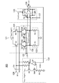
- FIG. 2 is a circuit diagram showing a first embodiment of the variable gain frequency converter 103 in FIG.
- the variable gain frequency converter 103 in FIG. 2 includes a frequency converter 121, a bias unit 122, a filter unit 123, an RF input terminal pair 124, an LO signal input terminal pair 125, an output terminal pair 126, and gain control. And a signal terminal 127.
- the frequency converter 121 includes a transconductor unit 131, a mixer core unit 132, and an output unit 133.
- the frequency converter 121 and the bias unit 122 operate at a high power supply voltage Vcc (HighV), and the filter unit 123 operates at a low power supply voltage Vcc (LowV).
- the RF input terminal pair 124 is connected to the variable gain LNA 102 of FIG. 1 and receives a differential RF input signal RFin.
- the LO signal input terminal pair 125 is connected to the 90-degree phase shifter 105 in FIG. 1 and receives a differential in-phase local oscillation signal (LOI signal).
- the output terminal pair 126 is connected to the variable gain amplifier 107 of FIG. 1 and outputs a baseband output signal BBout.
- the frequency converter gain control signal 116 of FIG. 1 is input to the gain control signal terminal 127.
- the transconductor unit 131 includes two P-type transistors M1 and M2, and converts the RF voltage signal supplied from the RF input terminal pair 124 via the coupling capacitor Cin into an RF current signal.
- the mixer core unit 132 includes four switch transistors SW1, SW2, SW3, and SW4, and a transconductor unit according to a normal rotation signal LO and an inverted signal LOB constituting a differential in-phase local oscillation signal (LOI signal).
- the frequency of the RF current signal output of 131 is converted into a baseband current signal.
- the output unit 133 includes two load resistors R1 and R2, and converts the baseband current signal output of the mixer core unit 132 into a baseband voltage signal.
- the filter unit 123 includes a differential amplifier including an input variable resistor Rin, a feedback resistor Rf, and a feedback capacitor Cf, and has a first-order LPF characteristic.
- the value of the input variable resistor Rin is controlled according to the frequency converter gain control signal 116 supplied to the gain control signal terminal 127.
- the output of the baseband voltage signal of the frequency converter 121 is amplified by the filter unit 123 according to the frequency converter gain control signal 116, and unnecessary waves are attenuated by the filter characteristic determined by the RC product of the filter unit 123, and the output terminal A baseband output signal BBout is output from the pair 126.
- the bias unit 122 includes an operational amplifier OP, a P-type transistor M0, a switch transistor SW0, a load resistor R0, and two bias resistors Rbias, and includes two P-type transistors M1, M1 constituting the transconductor unit 131. This determines the bias voltage of M2.
- the P-type transistor M0, the switch transistor SW0, and the load resistor R0 constitute a replica amplifier having the same circuit topology as that of the frequency converter 121.
- the operational amplifier OP is connected to the gate of the P-type transistor M0 so that the voltage at the connection node (corresponding to the output node of the frequency converter 121) between the switch transistor SW0 and the load resistor R0 matches the common voltage VCM of the filter unit 123.
- the voltage and the gate voltages of the two P-type transistors M1 and M2 in the transconductor unit 131 are controlled.
- the bias unit 122 applies feedback to the bias voltage of the frequency converter 121 so that the output voltage of the frequency converter 121 matches the common voltage VCM of the filter unit 123.
- the gate widths of the transistors M0 and SW0 of the replica amplifier are the transistors M1 and M2 of the frequency converter 121.
- SW1 to SW4 and 1 / A times the replica amplifier load resistance R0, and the load resistances R1 and R2 of the frequency converter 121 are set to A times the voltage of each node of the replica amplifier 121. Same as node voltage.
- a voltage that turns on the switch transistors SW1 to SW4 of the mixer core unit 132 is applied to the gate of the switch transistor SW0 of the replica amplifier.
- the operational amplifier OP of the bias unit 122 compares the voltage applied to the load resistance R0 of the replica amplifier with the common voltage VCM that determines the input / output voltage of the filter unit 123, and the gate of the P-type transistor M0 so that these voltages match. Adjust the voltage. By using the adjusted gate voltage as the bias voltage of the P-type transistors M1 and M2 in the frequency converter 121, the output voltage level of the frequency converter 121 is also equal to the common voltage VCM. As a result, the output voltage level of the frequency converter 121 matches the input / output voltage level of the filter unit 123.
- the power supply voltage of the filter unit 123 and the subsequent circuit is set lower than the power supply voltage of the frequency converter 121 and the previous circuit, the power supply voltage is different.
- the signal levels between the operating circuits can be made the same, and signals can be exchanged without any problem. Accordingly, a high power supply voltage is applied to the circuit before the frequency converter 121 to which a strong interference wave is input and a good distortion characteristic is required, thereby ensuring a wide dynamic range.
- a circuit having a thin film thickness by applying a low power supply voltage can be used for circuits after the filter unit 123 that requires good flicker noise characteristics. Therefore, even a high-performance direct conversion receiver that requires strict flicker noise characteristics and distortion characteristics can satisfy the required characteristics without problems.
- the value of the input variable resistor Rin of the filter unit 123 is controlled according to the frequency converter gain control signal 116 given to the gain control signal terminal 127.
- the transistor size of the frequency converter 121 and the load resistor R1 , R2 may be controlled. In that case, it is necessary to control the bias unit 122 according to the frequency converter gain control signal 116 as well.
- FIG. 3 is a circuit diagram showing a second embodiment of the variable gain frequency converter 103 in FIG.
- the variable gain frequency converter 103 of FIG. 3 includes a frequency converter 221, a bias unit 222, a filter unit 123, an RF input terminal pair 124, an LO signal input terminal pair 125, an output terminal pair 126, and gain control. And a signal terminal 127.
- the frequency converter 221 includes a transconductor unit 231, a mixer core unit 232, and an output unit 233.
- the frequency converter 221 and the bias unit 222 operate at a high power supply voltage Vcc (HighV), and the filter unit 123 operates at a low power supply voltage Vcc (LowV).
- the RF input terminal pair 124 is connected to the variable gain LNA 102 of FIG. 1 and receives a differential RF input signal RFin.
- the LO signal input terminal pair 125 is connected to the 90-degree phase shifter 105 in FIG. 1 and receives a differential in-phase local oscillation signal (LOI signal).
- the output terminal pair 126 is connected to the variable gain amplifier 107 of FIG. 1 and outputs a baseband output signal BBout.
- the frequency converter gain control signal 116 of FIG. 1 is input to the gain control signal terminal 127.
- the transconductor unit 231 includes four P-type transistors M1, M2, M3, and M4 and four N-type transistors M5, M6, M7, and M8.
- the RF signal input from the RF input terminal pair 124 is branched into a P-type transistor input signal and an N-type transistor input signal. Each branch is connected to the RF input terminal pair 124 via the coupling capacitors Cin1 and Cin2.
- the branched RF signals are amplified by the transconductor unit 231.
- the transconductor unit 231 in FIG. 3 has a current-reuse-type common-source amplifier configuration, and a part of the current flowing through the P-type transistor M1 (M2) flows to the N-type transistor M7 (M8). Gain is improved by supplying an RF signal to M7 (M2, M8). Furthermore, linearity is improved by connecting cascode transistors M3 and M5 (M4 and M6) to these P-type and N-type common source amplifiers. Here, voltages are supplied to the gates of the cascode transistors M3 and M5 (M4 and M6) so as to optimize the linearity of the amplification transistors M1 and M7 (M2 and M8), respectively. Further, if these transistors are connected in four stages, a wide dynamic range cannot be secured.
- the drain terminal of the N-type cascode transistor M5 (M6) is connected to the drain terminal of the P-type amplification transistor M1 (M2).
- the drain-source voltage of the P-type amplifying transistor M1 (M2) and the drain-source voltage of the N-type amplifying transistor M7 (M8) are secured by three-stage connection in the vertical stack, and the dynamic range is expanded.
- the mixer core unit 232 includes four switch transistors SW1, SW2, SW3, and SW4, and a transconductor unit according to a normal rotation signal LO and an inverted signal LOB that form a differential in-phase local oscillation signal (LOI signal).
- the RF current signal output of 231 is frequency converted into a baseband current signal.
- the output unit 233 includes two load resistors R1 and R2 and current sources I1 and I2 connected in parallel to the load resistors R1 and R2, and the baseband current signal output of the mixer core unit 232 is a baseband. Convert to voltage signal.
- the current source I1 in parallel with the load resistor R1 and connecting the current source I2 in parallel with the load resistor R2 and reducing the current flowing through the load resistors R1 and R2, the current of the mixer core 232 and the frequency conversion
- the load resistors R1 and R2 can be increased without changing the output level of the converter 221, and the gain of the frequency converter 221 determined by the product of the gm value of the transconductor portion 231 and the resistance value of the output portion 233 is increased. be able to.
- the frequency converter 221 having such a configuration, a wide dynamic range of the transconductor unit 231 can be secured, and the current of the mixer core unit 232, the magnitudes of the load resistors R1 and R2, and the output level of the frequency converter 221 can be determined. As compared with a Gilbert cell like the frequency converter 121 of FIG. That is, the gain, distortion characteristics, and output level of the frequency converter 221 can be appropriately designed.
- the filter unit 123 includes a differential amplifier including an input variable resistor Rin, a feedback resistor Rf, and a feedback capacitor Cf, and has a first-order LPF characteristic.
- the value of the input variable resistor Rin is controlled according to the frequency converter gain control signal 116 supplied to the gain control signal terminal 127.
- the baseband voltage signal output of the frequency converter 221 is amplified by the filter unit 123 according to the frequency converter gain control signal 116, and the unnecessary wave is attenuated by the filter characteristic determined by the RC product of the filter unit 123, and the output terminal A baseband output signal BBout is output from the pair 126.
- the bias unit 222 includes an operational amplifier OP, P-type transistors M0 and M9, N-type transistors M10 and M11, a switch transistor SW0, a load resistor R0, a current source I0, two bias resistors Rbias1, and other components. It consists of two bias resistors Rbias2, determines the bias voltage of the two P-type transistors M1 and M2 constituting the transconductor portion 231 and applies the bias voltage of the two N-type transistors M7 and M8. is there.
- the P-type transistors M0 and M9, the N-type transistors M10 and M11, the switch transistor SW0, the load resistor R0, and the current source I0 constitute a replica amplifier having the same circuit topology as the frequency converter 221.
- the operational amplifier OP is a gate of the P-type transistor M0 so that the voltage of the connection node (corresponding to the output node of the frequency converter 221) between the switch transistor SW0 and the load resistor R0 matches the common voltage VCM of the filter unit 123.
- the voltage and the gate voltages of the two P-type transistors M1 and M2 in the transconductor unit 231 are controlled. In this way, the bias unit 222 feeds back the bias voltage of the frequency converter 221 so that the output voltage of the frequency converter 221 matches the common voltage VCM of the filter unit 123.
- the gate widths of the transistors M0, M9, M10, M11, and SW0 of the replica amplifier are frequency converters.
- the voltage at each node of the replica amplifier is set to 1 / A times that of the transistors M1 to M8 and SW1 to SW4 of the 221 and the load resistance R0 of the replica amplifier is set to A times the load resistances R1 and R2 of the frequency converter 221. This is the same as the voltage at each node of the frequency converter 221.
- a voltage that turns on the switch transistors SW1 to SW4 of the mixer core unit 232 is applied to the gate of the switch transistor SW0 of the replica amplifier.
- the gate voltage of the P-type transistor M9 gives the same voltage as the gate voltage of the P-type transistors M3 and M4, and the gate voltage of the N-type transistor M10 gives the same voltage as the gate voltage of the N-type transistors M5 and M6.
- the operational amplifier OP of the bias unit 222 compares the voltage applied to the load resistor R0 of the replica amplifier with the common voltage VCM that determines the input / output voltage of the filter unit 123, and the gate of the P-type transistor M0 so that these voltages match. Adjust the voltage. By using the adjusted gate voltage as the bias voltage of the P-type transistors M1 and M2 in the frequency converter 221, the output voltage level of the frequency converter 221 becomes equal to the common voltage VCM. As a result, the output voltage level of the frequency converter 221 matches the input / output voltage level of the filter unit 123.
- the power supply voltage of the filter unit 123 and the subsequent circuit is set lower than the power supply voltage of the frequency converter 221 and the previous circuit, the power supply voltage is different.
- the signal levels between the operating circuits can be made the same, and signals can be exchanged without any problem. Accordingly, a high power supply voltage is applied to a circuit before the frequency converter 221 to which a strong interference wave is input and a good distortion characteristic is required to ensure a wide dynamic range.
- a circuit having a thin film thickness by applying a low power supply voltage can be used for circuits after the filter unit 123 that requires good flicker noise characteristics. Therefore, even a high-performance direct conversion receiver that requires strict flicker noise characteristics and distortion characteristics can satisfy the required characteristics without problems.
- the feedback in the bias unit 222 may adjust the bias voltage of the N-type transistor M11 while keeping the bias voltage of the P-type transistor M0 constant.
- the value of the input variable resistor Rin of the filter unit 123 is controlled according to the frequency converter gain control signal 116 applied to the gain control signal terminal 127.
- the transistor size of the frequency converter 221 and the load resistor R1 , R2 or the values of the current sources I1, I2 may be controlled. In that case, it is necessary to control the bias unit 222 according to the frequency converter gain control signal 116 as well.
- FIG. 4 is a circuit diagram showing a third embodiment of the variable gain frequency converter 103 in FIG.
- the variable gain frequency converter 103 of FIG. 4 includes a frequency converter 321, a bias unit 322, a filter unit 123, an RF input terminal pair 124, an LO signal input terminal pair 125, an output terminal pair 126, and gain control. And a signal terminal 127.
- the frequency converter 321 includes a transconductor unit 331, a mixer core unit 332, and an output unit 333, and is a passive mixer that does not flow a steady current through the mixer core unit 332.
- the frequency converter 321 and the bias unit 322 operate at a high power supply voltage Vcc (High V), and the filter unit 123 operates at a low power supply voltage Vcc (Low V).
- the RF input terminal pair 124 is connected to the variable gain LNA 102 of FIG. 1 and receives a differential RF input signal RFin.
- the LO signal input terminal pair 125 is connected to the 90-degree phase shifter 105 in FIG. 1 and receives a differential in-phase local oscillation signal (LOI signal).
- the output terminal pair 126 is connected to the variable gain amplifier 107 of FIG. 1 and outputs a baseband output signal BBout.
- the frequency converter gain control signal 116 of FIG. 1 is input to the gain control signal terminal 127.
- the transconductor section 331 is composed of two P-type transistors M1 and M2, the mixer core section 332 is composed of four switch transistors SW1, SW2, SW3, and SW4, and the output section 333 is composed of two load resistors R1 and R2. .
- the RF signal input from the RF input terminal pair 124 is input to the transconductor unit 331 after capacitive coupling, and is amplified by the gm of the transconductor unit 331 and the load resistors R1 and R2 of the output unit 333.
- the mixer core unit 332 converts the frequency of the RF signal output from the output unit 333 into a baseband signal in accordance with the differential in-phase local oscillation signal (LOI signal).
- LOI signal differential in-phase local oscillation signal
- the filter unit 123 includes a differential amplifier including an input variable resistor Rin, a feedback resistor Rf, and a feedback capacitor Cf, and has a first-order LPF characteristic.
- the value of the input variable resistor Rin is controlled according to the frequency converter gain control signal 116 supplied to the gain control signal terminal 127.
- the baseband voltage signal output of the frequency converter 321 is amplified by the filter unit 123 in accordance with the frequency converter gain control signal 116, and unnecessary waves are attenuated by the filter characteristic determined by the RC product of the filter unit 123, and the output terminal A baseband output signal BBout is output from the pair 126.
- the bias unit 322 includes an operational amplifier OP, a P-type transistor M0, a load resistor R0, and two bias resistors Rbias.
- the bias unit 322 determines the bias voltage of the two P-type transistors M1 and M2 constituting the transconductor unit 331. To decide. Among these, the P-type transistor M0 and the load resistor R0 constitute a replica amplifier having the same circuit topology as the frequency converter 321.
- the operational amplifier OP includes the gate voltage of the P-type transistor M0 and the two voltages in the transconductor unit 331 so that the voltage at the connection node between the P-type transistor M0 and the load resistor R0 matches the common voltage VCM of the filter unit 123.
- the gate voltages of the P-type transistors M1 and M2 are controlled. In this way, the bias unit 322 feeds back the bias voltage of the frequency converter 321 so that the output voltage of the frequency converter 321 matches the common voltage VCM of the filter unit 123.
- the gate width of the transistor M0 of the replica amplifier is set to 1 of the transistors M1 and M2 of the frequency converter 321.
- the voltage of each node of the replica amplifier is made the same as the voltage of each node of the frequency converter 321 by setting the load resistance R0 of the replica amplifier to A times the load resistances R1 and R2 of the frequency converter 321. .
- the operational amplifier OP of the bias unit 322 compares the voltage applied to the load resistance R0 of the replica amplifier with the common voltage VCM that determines the input / output voltage of the filter unit 123, and the gate of the P-type transistor M0 so that these voltages match. Adjust the voltage. By using the adjusted gate voltage as the bias voltage of the P-type transistors M1 and M2 in the frequency converter 321, the output voltage level of the frequency converter 321 is also equal to the common voltage VCM. As a result, the output voltage level of the frequency converter 321 matches the input / output voltage level of the filter unit 123.
- the frequency converter 321 can be connected to the filter unit 123 without capacitive coupling between the output unit 333 and the mixer core unit 332, and a steady current can be prevented from flowing through the mixer core unit 332.
- the flicker noise characteristic of the mixer core unit 332 can be improved.
- the power supply voltage of the filter unit 123 and the subsequent circuit is set lower than the power supply voltage of the frequency converter 321 and the previous circuit, the power supply voltage is different.
- the signal levels between the operating circuits can be made the same, and signals can be exchanged without any problem. Therefore, a high power supply voltage is applied to a circuit before the frequency converter 321 to which a strong interference wave is input and a good distortion characteristic is required, thereby ensuring a wide dynamic range.
- a circuit having a thin film thickness by applying a low power supply voltage can be used for circuits after the filter unit 123 that requires good flicker noise characteristics. Therefore, even a high-performance direct conversion receiver that requires strict flicker noise characteristics and distortion characteristics can satisfy the required characteristics without problems.
- the value of the input variable resistor Rin of the filter unit 123 is controlled according to the frequency converter gain control signal 116 given to the gain control signal terminal 127, but the transistor size of the frequency converter 321 and the load resistor R1 , R2 may be controlled. In that case, it is necessary to control the bias unit 322 according to the frequency converter gain control signal 116 as well.
- variable gain frequency converter 103 has the same configuration.
- LOQ signal quadrature local oscillation signal
- LOI signal in-phase local oscillation signal
- the filter unit 123 is a first-order LPF, it may be a higher-order Butterworth filter, a Chebyshev filter, or an elliptic filter.
- an RF signal is input from the antenna 100, but a signal input by wired connection may be used.
- the balun 101 converts the signal into a differential signal.
- the balun 101 may be used instead of a single-phase signal.
- variable gain LNA 102 is used, but an LNA having a fixed gain may be used instead.
- an amplifier having a fixed gain may be used instead of the variable gain amplifiers 107 and 108.
- the digital signal processing unit 113 compares the output signal level with the reference level.
- the result of monitoring the block output level may be compared with the reference level.
- the present invention relates to a direct conversion receiver used in a communication system or a broadcasting system, and has good flicker noise characteristics, and is useful as a TV tuner, a portable terminal, and the like.
Landscapes
- Engineering & Computer Science (AREA)
- Power Engineering (AREA)
- Computer Networks & Wireless Communication (AREA)
- Signal Processing (AREA)
- Superheterodyne Receivers (AREA)
- Amplifiers (AREA)
- Circuits Of Receivers In General (AREA)
Abstract
La présente invention a pour objectif de proposer un récepteur à conversion directe dont le rapport signal sur bruit plus distorsion (SNDR) est amélioré et dont les caractéristiques de bruit de scintillation sont elles aussi améliorées sans pour autant renchérir le coût de la puce ou dégrader les caractéristiques de distorsion. Afin atteindre l'objectif visé, la présente invention exécute les opérations suivantes : elle relève la tension d'alimentation d'un convertisseur de fréquence (121), dans lequel une onde brouilleuse de forte intensité est entrée, afin de sécuriser une plage dynamique étendue ; elle diminue la tension d'alimentation d'un module de filtrage (123), dont on exige des caractéristiques de bruit de scintillation strictes, pour utiliser un transistor à couches minces ; et elle ajuste un niveau de signal entre les différents circuits de tension d'alimentation au moyen d'un module de polarisation qui utilise la rétroaction.
Priority Applications (1)
| Application Number | Priority Date | Filing Date | Title |
|---|---|---|---|
| JP2014516634A JPWO2013175681A1 (ja) | 2012-05-22 | 2013-03-06 | ダイレクトコンバージョン方式の受信機 |
Applications Claiming Priority (2)
| Application Number | Priority Date | Filing Date | Title |
|---|---|---|---|
| JP2012116226 | 2012-05-22 | ||
| JP2012-116226 | 2012-05-22 |
Publications (1)
| Publication Number | Publication Date |
|---|---|
| WO2013175681A1 true WO2013175681A1 (fr) | 2013-11-28 |
Family
ID=49623397
Family Applications (1)
| Application Number | Title | Priority Date | Filing Date |
|---|---|---|---|
| PCT/JP2013/001408 Ceased WO2013175681A1 (fr) | 2012-05-22 | 2013-03-06 | Récepteur à conversion directe |
Country Status (2)
| Country | Link |
|---|---|
| JP (1) | JPWO2013175681A1 (fr) |
| WO (1) | WO2013175681A1 (fr) |
Cited By (2)
| Publication number | Priority date | Publication date | Assignee | Title |
|---|---|---|---|---|
| EP3229372A1 (fr) * | 2016-04-06 | 2017-10-11 | NXP USA, Inc. | Système et procédé pour coupler directement un convertisseur analogique vers numérique à référence de tension inférieure |
| CN111200404A (zh) * | 2018-11-16 | 2020-05-26 | 财团法人工业技术研究院 | 线性度改善系统及线性度改善方法 |
Citations (3)
| Publication number | Priority date | Publication date | Assignee | Title |
|---|---|---|---|---|
| JP2003204224A (ja) * | 2001-10-22 | 2003-07-18 | Fujitsu Ltd | ミキサ回路、受信回路、及び周波数比較回路 |
| JP2008219623A (ja) * | 2007-03-06 | 2008-09-18 | Handotai Rikougaku Kenkyu Center:Kk | 周波数変換回路 |
| JP2011216982A (ja) * | 2010-03-31 | 2011-10-27 | Fujitsu Semiconductor Ltd | ミキサ回路及びミキサ回路のコモン電圧調整方法 |
-
2013
- 2013-03-06 JP JP2014516634A patent/JPWO2013175681A1/ja active Pending
- 2013-03-06 WO PCT/JP2013/001408 patent/WO2013175681A1/fr not_active Ceased
Patent Citations (3)
| Publication number | Priority date | Publication date | Assignee | Title |
|---|---|---|---|---|
| JP2003204224A (ja) * | 2001-10-22 | 2003-07-18 | Fujitsu Ltd | ミキサ回路、受信回路、及び周波数比較回路 |
| JP2008219623A (ja) * | 2007-03-06 | 2008-09-18 | Handotai Rikougaku Kenkyu Center:Kk | 周波数変換回路 |
| JP2011216982A (ja) * | 2010-03-31 | 2011-10-27 | Fujitsu Semiconductor Ltd | ミキサ回路及びミキサ回路のコモン電圧調整方法 |
Cited By (5)
| Publication number | Priority date | Publication date | Assignee | Title |
|---|---|---|---|---|
| EP3229372A1 (fr) * | 2016-04-06 | 2017-10-11 | NXP USA, Inc. | Système et procédé pour coupler directement un convertisseur analogique vers numérique à référence de tension inférieure |
| CN107276592A (zh) * | 2016-04-06 | 2017-10-20 | 恩智浦美国有限公司 | 直接耦合到具有较低电压参考的模数转换器的系统和方法 |
| US9923532B2 (en) | 2016-04-06 | 2018-03-20 | Nxp Usa, Inc. | System and method to directly couple to analog to digital converter having lower voltage reference |
| CN107276592B (zh) * | 2016-04-06 | 2023-06-27 | 恩智浦美国有限公司 | 模数转换器、将可变增益放大器与模数转换器介接的方法 |
| CN111200404A (zh) * | 2018-11-16 | 2020-05-26 | 财团法人工业技术研究院 | 线性度改善系统及线性度改善方法 |
Also Published As
| Publication number | Publication date |
|---|---|
| JPWO2013175681A1 (ja) | 2016-01-12 |
Similar Documents
| Publication | Publication Date | Title |
|---|---|---|
| US7880546B2 (en) | Amplifier and the method thereof | |
| JP5355366B2 (ja) | 差動増幅回路および無線受信機 | |
| CN101627535A (zh) | 具有宽带阻抗和噪声匹配的频率选择性放大器 | |
| CN111434031A (zh) | 功率放大器电路 | |
| US8159619B2 (en) | Multi-standard integrated television receiver | |
| US8050642B2 (en) | Variable gain amplifier and receiver including the same | |
| JPWO2007026572A1 (ja) | 低雑音増幅回路、および受信システム | |
| US9503053B1 (en) | Active balun for wideband applications | |
| KR101127461B1 (ko) | 고도의 선형 가변이득 증폭기 | |
| US7139544B2 (en) | Direct down-conversion receiver with transconductance-capacitor filter and method | |
| US20090027128A1 (en) | Variable gain amplifier | |
| CN111294012B (zh) | 电容器电路及电容倍增式滤波器 | |
| CN111903119B (zh) | 一种全频带接收机和电视调谐器 | |
| JP2015170892A (ja) | 低雑音増幅回路 | |
| WO2013175681A1 (fr) | Récepteur à conversion directe | |
| JP5433614B2 (ja) | 半導体集積回路および受信装置 | |
| US20150070055A1 (en) | Receiver | |
| JP2008270924A (ja) | 周波数変換回路および受信装置 | |
| JP2011205229A (ja) | 無線受信回路 | |
| WO2015019525A1 (fr) | Circuit amplificateur à transconductance de type cascode et à gain variable, et système syntoniseur équipé de celui-ci | |
| JP2013225798A (ja) | Dcオフセット除去回路 | |
| CN112262531B (zh) | 环通输出电路、电视调谐器和射频接收系统 | |
| Özkan et al. | A Highly Linear Passive Attenuator and Mixer Designs for an Observation Receiver in 130‐nm SOI CMOS | |
| JP2016115977A (ja) | 受信装置及びその歪み抑圧方法、半導体装置並びに電子機器 | |
| Keping et al. | Noise-canceling and IP3 improved CMOS RF front-end for DRM/DAB/DVB-H applications |
Legal Events
| Date | Code | Title | Description |
|---|---|---|---|
| 121 | Ep: the epo has been informed by wipo that ep was designated in this application |
Ref document number: 13793109 Country of ref document: EP Kind code of ref document: A1 |
|
| ENP | Entry into the national phase |
Ref document number: 2014516634 Country of ref document: JP Kind code of ref document: A |
|
| NENP | Non-entry into the national phase |
Ref country code: DE |
|
| 122 | Ep: pct application non-entry in european phase |
Ref document number: 13793109 Country of ref document: EP Kind code of ref document: A1 |