WO2013175943A1 - Module composé - Google Patents
Module composé Download PDFInfo
- Publication number
- WO2013175943A1 WO2013175943A1 PCT/JP2013/062522 JP2013062522W WO2013175943A1 WO 2013175943 A1 WO2013175943 A1 WO 2013175943A1 JP 2013062522 W JP2013062522 W JP 2013062522W WO 2013175943 A1 WO2013175943 A1 WO 2013175943A1
- Authority
- WO
- WIPO (PCT)
- Prior art keywords
- substrate
- case
- electronic component
- component element
- board
- Prior art date
- Legal status (The legal status is an assumption and is not a legal conclusion. Google has not performed a legal analysis and makes no representation as to the accuracy of the status listed.)
- Ceased
Links
Images


Classifications
-
- H—ELECTRICITY
- H05—ELECTRIC TECHNIQUES NOT OTHERWISE PROVIDED FOR
- H05K—PRINTED CIRCUITS; CASINGS OR CONSTRUCTIONAL DETAILS OF ELECTRIC APPARATUS; MANUFACTURE OF ASSEMBLAGES OF ELECTRICAL COMPONENTS
- H05K7/00—Constructional details common to different types of electric apparatus
- H05K7/20—Modifications to facilitate cooling, ventilating, or heating
- H05K7/2039—Modifications to facilitate cooling, ventilating, or heating characterised by the heat transfer by conduction from the heat generating element to a dissipating body
- H05K7/20509—Multiple-component heat spreaders; Multi-component heat-conducting support plates; Multi-component non-closed heat-conducting structures
-
- H—ELECTRICITY
- H05—ELECTRIC TECHNIQUES NOT OTHERWISE PROVIDED FOR
- H05K—PRINTED CIRCUITS; CASINGS OR CONSTRUCTIONAL DETAILS OF ELECTRIC APPARATUS; MANUFACTURE OF ASSEMBLAGES OF ELECTRICAL COMPONENTS
- H05K5/00—Casings, cabinets or drawers for electric apparatus
- H05K5/02—Details
- H05K5/0256—Details of interchangeable modules or receptacles therefor, e.g. cartridge mechanisms
- H05K5/026—Details of interchangeable modules or receptacles therefor, e.g. cartridge mechanisms having standardized interfaces
- H05K5/0278—Details of interchangeable modules or receptacles therefor, e.g. cartridge mechanisms having standardized interfaces of USB type
-
- H—ELECTRICITY
- H05—ELECTRIC TECHNIQUES NOT OTHERWISE PROVIDED FOR
- H05K—PRINTED CIRCUITS; CASINGS OR CONSTRUCTIONAL DETAILS OF ELECTRIC APPARATUS; MANUFACTURE OF ASSEMBLAGES OF ELECTRICAL COMPONENTS
- H05K7/00—Constructional details common to different types of electric apparatus
- H05K7/02—Arrangements of circuit components or wiring on supporting structure
- H05K7/026—Multiple connections subassemblies
-
- H—ELECTRICITY
- H05—ELECTRIC TECHNIQUES NOT OTHERWISE PROVIDED FOR
- H05K—PRINTED CIRCUITS; CASINGS OR CONSTRUCTIONAL DETAILS OF ELECTRIC APPARATUS; MANUFACTURE OF ASSEMBLAGES OF ELECTRICAL COMPONENTS
- H05K7/00—Constructional details common to different types of electric apparatus
- H05K7/20—Modifications to facilitate cooling, ventilating, or heating
- H05K7/2039—Modifications to facilitate cooling, ventilating, or heating characterised by the heat transfer by conduction from the heat generating element to a dissipating body
- H05K7/20436—Inner thermal coupling elements in heat dissipating housings, e.g. protrusions or depressions integrally formed in the housing
- H05K7/20445—Inner thermal coupling elements in heat dissipating housings, e.g. protrusions or depressions integrally formed in the housing the coupling element being an additional piece, e.g. thermal standoff
-
- H—ELECTRICITY
- H05—ELECTRIC TECHNIQUES NOT OTHERWISE PROVIDED FOR
- H05K—PRINTED CIRCUITS; CASINGS OR CONSTRUCTIONAL DETAILS OF ELECTRIC APPARATUS; MANUFACTURE OF ASSEMBLAGES OF ELECTRICAL COMPONENTS
- H05K7/00—Constructional details common to different types of electric apparatus
- H05K7/20—Modifications to facilitate cooling, ventilating, or heating
- H05K7/2039—Modifications to facilitate cooling, ventilating, or heating characterised by the heat transfer by conduction from the heat generating element to a dissipating body
- H05K7/20436—Inner thermal coupling elements in heat dissipating housings, e.g. protrusions or depressions integrally formed in the housing
- H05K7/20445—Inner thermal coupling elements in heat dissipating housings, e.g. protrusions or depressions integrally formed in the housing the coupling element being an additional piece, e.g. thermal standoff
- H05K7/20472—Sheet interfaces
-
- H—ELECTRICITY
- H04—ELECTRIC COMMUNICATION TECHNIQUE
- H04B—TRANSMISSION
- H04B1/00—Details of transmission systems, not covered by a single one of groups H04B3/00 - H04B13/00; Details of transmission systems not characterised by the medium used for transmission
- H04B1/38—Transceivers, i.e. devices in which transmitter and receiver form a structural unit and in which at least one part is used for functions of transmitting and receiving
- H04B1/3827—Portable transceivers
- H04B1/3888—Arrangements for carrying or protecting transceivers
Definitions
- the present invention relates to a composite module equipped with a high heat generation electronic component element, and more particularly to a wireless LAN module, for example.
- Patent Document 1 describes an electronic device that is composed of two substrates, a multilayer substrate and a metal base substrate, and an electronic component element is mounted on each substrate.
- an electronic component element that generates heat is mounted on a multilayer substrate, and a heat dissipation sheet is disposed immediately above the electronic component element (that is, a surface facing the mounting surface of the electronic component element).
- Patent Document 1 describes a structure in which heat generated from an electronic component element is radiated to a metal base substrate via a heat dissipation sheet. With such a structure, heat generated from the electronic component element can be effectively radiated to the metal base substrate, and deterioration of characteristics of the electronic component element due to the heat generation can be prevented.
- the main object of the present invention is to efficiently dissipate the heat generated inside the composite module, thereby making it possible to prevent deterioration of the characteristics of the electronic component elements mounted on the module and the composite module. To provide a composite module.
- the composite module according to the present invention includes a first substrate and an external connection connector mounted on one main surface of the first substrate, the other main surface of the first substrate, An electronic component element is disposed in a region facing a connector for external connection with a substrate interposed therebetween.
- an electronic component element is mounted on the other main surface of the first substrate.
- the composite module according to the present invention includes a second substrate disposed so as to face the other main surface of the first substrate, and the electronic component element is mounted on the one main surface of the second substrate. It is preferable.
- the composite module according to the present invention includes a board connection connector for mechanically connecting the first board and the second board, and the external connection connector is provided on one end side of the first board.
- the mounted connector for board connection is disposed on the other end side of the other main surface of the first board.
- the heat radiating member is arrange
- the heat dissipating member is arranged so as to contact the surface opposite to the mounting surface of the electronic component element and the other main surface of the first substrate.
- the composite module according to the above-described invention further includes an antenna and a case, the case houses the composite module and the antenna, and the inner wall surface of the case is the composite module.
- a portion near the electronic component element disposed in a region facing the external connection connector across the first substrate, the first substrate and the second substrate being It is preferable to provide a cutout portion on at least one of the first substrate and the second substrate for preventing at least one of them from contacting the inner wall surface of the case.
- a composite module according to the present invention includes an external connection connector mounted on one main surface of a first board, and is on the other main surface of the first board and is used for external connection across the first board. Since the electronic component element is arranged or mounted in a region facing the connector, the heat generated in the electronic component element is transferred to the external connector via the first substrate, and the heat transferred is combined. Since heat is radiated to the electronic device to which the module is connected via the external connection connector, heat generated in the electronic component element can be efficiently radiated.
- the composite module according to the present invention includes a second substrate disposed so as to face the other main surface of the first substrate, and an electronic component element is mounted on the one main surface of the second substrate.
- the composite module according to the present invention includes a board connection connector for mechanically connecting the first board and the second board, and the external connection connector is provided on one end side of the first board.
- the mounted connector for board connection is arranged on the other end side of the other main surface of the first board, so that the mechanical strength of the composite module is improved and the heat capacity is also improved by providing the board connection connector.
- heat transfer from the second substrate to the first substrate generated in the electronic component element can be efficiently performed via the substrate connecting connector. Therefore, the heat generated in the electronic component element can be radiated more efficiently.
- the heat radiating member is disposed on the surface opposite to the mounting surface of the electronic component element, or the surface opposite to the mounting surface of the electronic component element and the first substrate. Since the heat radiating member is disposed so as to be in contact with the other main surface, the heat generated in the electronic component element is transferred to the heat radiating member, and further, the heat transferred to the heat radiating member is By transferring heat to the external connection connector, heat is radiated to the electronic device to which the composite module is connected via the external connection connector, so that heat generated in the electronic component element can be radiated more efficiently. .
- the composite module according to the present invention includes the composite module according to the above-described invention, further including an antenna and a case, wherein the case houses the composite module and the antenna, and the inner wall surface of the case includes the composite module. Since it is in contact with the antenna via the antenna, the above-described effects are achieved, the heat capacity of the composite module is improved, and the heat generated in the electronic component element is dissipated to the case side via the antenna. Heat generated in the component element can be radiated more efficiently. Furthermore, the composite module according to the present invention is a vicinity of an electronic component element disposed in a region facing the external connection connector with the first substrate interposed therebetween, and includes the first substrate and the second substrate.
- the heat generated from the electronic component element is It is possible to have a composite module structure that makes it difficult to radiate heat from at least one of the first substrate and the second substrate directly to the case side and efficiently radiates heat through the external connection connector. .
- a composite module that makes it possible to prevent deterioration of characteristics of electronic component elements and composite modules mounted on the module by efficiently dissipating heat generated inside the composite module. can do.
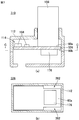
- FIG. 1 is a plan view of a board portion in a first embodiment of a wireless LAN module according to the present invention, (a) is a plan view of a first board, and (b) is a plan view of a second board. . It is a cross-sectional schematic diagram about 2nd Embodiment of the wireless LAN module concerning this invention. It is a cross-sectional schematic diagram about 3rd Embodiment of the wireless LAN module concerning this invention.
- FIG. 5A is a plan sectional view taken along line AA in FIG. 5 and FIG. 5B is a plan sectional view taken along line BB in FIG. 5 for a third embodiment of the wireless LAN module according to the present invention.
- (A) is a schematic cross-sectional view of a wireless LAN module according to a fourth embodiment of the present invention, and (b) is a cross-sectional plan view taken along the line CC.
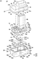
- FIG. 1 is an exploded perspective view of a wireless LAN module according to a first embodiment of the present invention.
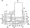
- FIG. 2 is a schematic sectional view of the wireless LAN module according to the first embodiment of the present invention.
- the wireless LAN module 10 is a module for enabling a wireless communication function to be exerted on the electronic device by connecting to the electronic device, for example.
- the wireless LAN module 10 illustrated in FIG. 1 includes at least a case 12 and a substrate unit 14.
- the wireless LAN module 10 further includes a button member 16, a lens member 18, and an antenna 20.
- the case 12 is provided to accommodate at least the substrate part 14.
- the case 12 is provided for housing the button member 16, the lens member 18, and the antenna 20.
- the case 12 is formed in a rectangular parallelepiped shape.
- the case 12 includes a first case 22 and a second case 24.
- substrate part 14 contains the 1st board
- the first case 22 is formed in a box shape by the side surface portion 30 and the upper surface portion 32.
- the side surface portion 30 of the first case 22 includes one side surface 34a and the other side surface 34b extending along the long side direction and the height direction.
- the one side surface 34a and the other side surface 34b are formed to face each other.
- a rectangular opening 36 is formed on the lower side of the first case 22 (the side facing the upper surface portion 32).
- a groove 36 a having an L-shaped cross section is formed along the inner surface of the opening 36.
- a storage portion 38 is provided inside the box formed by the side surface portion 30 and the upper surface portion 32 of the first case 22.
- an inner wall surface 40 is formed on the surface of the side surface portion 30 on the storage portion 38 side.
- a plurality of substrate protrusions 42 for supporting the substrate portion 14 are formed on the inner wall surface 40.
- the substrate projection 42 is formed in a bar shape having a substantially circular cross section having one end and the other end.
- the board projections 42 formed on the first case 22 are provided to support the one main surface 72a of the second board 28 of the board 14 so as to be pressed.
- the substrate projections 42 are formed at two locations on the inner wall surface 40 of the first side surface 34a of the first case 22 at a predetermined interval, and the inner wall surface 40 of the other side surface 34b is 1
- the substrate protrusion 42 is formed.
- the length of the board protrusion 42 is, for example, longer than the length of the opening 36 from the upper surface 32 of the first case 22, and the length of the second board 28 inside the case 12 is determined by this length. The position in the thickness direction is determined.
- a connector opening 32 a is formed in the upper surface portion 32 of the first case 22.
- the connector opening 32a is formed to penetrate an external connection connector 66 described later.
- a cylindrical tube portion 32b is formed to support the external connection connector 66.
- the second case 24 is formed in a box shape by the side surface portion 44 and the bottom surface portion 46.
- the side surface portion 44 of the second case 24 includes one side surface 48a and the other side surface 48b extending along the long side direction and the height direction, and the one end surface 50a and the other side extending along the short side direction and the height direction.
- the end surface 50b is included.
- One side surface 48a and the other side surface 48b are formed to face each other, and one end surface 50a and the other end surface 50b are also formed to face each other.
- the bottom surface portion 46 is formed with a button opening 46a and a lens opening 46b.
- a rectangular opening 52 is formed on the upper side of the second case 24 (the side facing the bottom surface 46).
- a protruding edge portion 52 a is formed along the substantially inner edge of the opening 52.
- a storage portion 54 is provided inside the second case 24 formed in a box shape by the side surface portion 44 and the bottom surface portion 46.
- an inner wall surface 56 is formed on a surface of the side surface portion 44 on the storage portion 54 side.
- a plurality of substrate projections 58 for supporting the substrate portion 14 are formed on the inner wall surface 56.
- the substrate projections 58 formed on the second case 24 include the first substrate projections 58a for supporting the first substrate 26 of the substrate unit 14 and the second substrate of the substrate unit 14. And a second substrate projection 58b for supporting the 28.
- the first substrate projection 58a and the second substrate projection 58b are each formed in a bar shape having a substantially circular cross section having one end and the other end.
- one location is provided on the inner wall surface 56 on the one side surface 48a of the second case 24, one location is provided on the inner wall surface 56 on the other side surface 48b, and one location is provided on the inner wall surface 56 on the one end surface 50a.
- a first substrate projection 58a is formed.
- the first substrate projection 58 a is formed to have a length from the bottom surface 46 to the opening 52 of the second case 24, for example.
- the lengths of the first substrate projections 58a are the same.
- the position of the first substrate 26 in the thickness direction within the case 12 is determined by the length of the first substrate projection 58a.
- the second substrate projection 58b is provided at one position on the inner wall surface 56 at a position different from the first substrate projection 58a, that is, at a predetermined interval from the first substrate projection 58a. It is formed.
- the second substrate projection 58b is formed to have an intermediate length between the bottom surface 46 and the opening 52 of the second case 24, for example. The lengths of the respective second substrate projections 58b are the same.
- the position of the second substrate 28 in the thickness direction within the case 12 is determined by the length of the second substrate projection 58b.
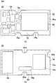
- FIG. 3 is a plan view of a substrate portion in the first embodiment of the wireless LAN module according to the present invention
- FIG. 3A is a plan view of the first substrate
- FIG. It is a top view of the board
- FIG. The substrate unit 14 includes a first substrate 26 and a second substrate 28.
- substrate 28 are formed with a printed circuit board etc., for example. Further, the thickness of the first substrate 26 is formed to be thicker than the thickness of the second substrate 28.
- the first substrate 26 is formed in a rectangular plate shape and includes one main surface 60a and the other main surface 60b.
- a first functional block 62 for realizing a predetermined function is disposed on the one main surface 60a of the first substrate 26.
- the first functional block 62 has a wiring pattern (not shown) and an electronic component element 64 is mounted thereon. ing.
- the electronic component element 64 mounted on the first functional block 62 is, for example, an electronic component element 64 related to a power supply circuit.
- the electronic component element 64 is, for example, a coil component such as a DC-DC converter. Therefore, when the first substrate 26 is stored in the case 12, the upper surface portion 32 of the first case 22 and the electronic component element 64 related to the power supply circuit mounted on the first functional block 62 are opposed to each other. Be placed.
- a connection connector 66 is mounted in one area of the one main surface 60a of the first substrate 26 and outside the area where the electronic component element 64 related to the power circuit mounted on the first functional block 62 is mounted.
- the external connector 66 for example, a 5-pin or 8-pin USB connector is used.
- the other end side of the first substrate 26 with respect to the other main surface 60b is mechanically connected to the first substrate 26 and the second substrate 28 with a desired interval in the thickness direction of each substrate.
- a board connecting connector 68 is provided.
- an edge portion 70 is provided along the outer periphery of the first substrate 26.
- a plurality of, for example, semicircular recesses 70 a are formed on the edge portion 70 of the first substrate 26 corresponding to the substrate projections 42 formed on the first case 22.
- a total of three recesses 70a are provided on each long side of the edge portion 70. Therefore, the board projections 42 formed in the first case 22 are inserted into the recesses 70a.
- the end edge portion 70 of the other main surface 60 b of the first substrate 26 is supported by one end of the first substrate projection 58 a formed at three locations on the inner wall surface 40 of the second case 24. Supported by
- the second substrate 28 is formed in a rectangular plate shape and includes one main surface 72a and the other main surface 72b.
- the one main surface 72a of the second substrate 28 is arranged with a desired interval in the thickness direction of each substrate through the substrate connecting connector 68 so as to face the other main surface 60b of the first substrate 26.
- the size of the outer shape of the second substrate 28 is substantially the same as the size of the first substrate 26.
- a second functional block 74 for realizing a predetermined function different from the first functional block 62 is disposed on the one main surface 72a of the second substrate 28, and a wiring pattern (not shown) is provided.
- the electronic component elements 76a and 76b are mounted.
- the electronic component element 64 mounted on the first functional block 62 and the electronic component elements 76a and 76b mounted on the second functional block 74 are arranged, for example, with the first substrate 26 interposed therebetween. Therefore, they are not arranged so as to face each other directly.
- the electronic component elements 76a and 76b mounted on the second functional block 74 are, for example, electronic component elements related to a control circuit such as a wireless LAN IC or MCU (micro control unit).
- the other main surface 60b of the first substrate 26 on which the external connection connector 66 is mounted is an area facing the first substrate 26 with the first main surface 72a of the second substrate 28 facing the one main surface 72a.
- the component element 76a is arranged.
- the electronic component element 76 a is mounted on the one main surface 72 a of the second substrate 28 in a region immediately below the surface on which the external connection connector 66 is mounted.
- the electronic component element 76a mounted on the second functional block 74 is an electronic component element that generates relatively high heat.
- the writing mode and the reading mode are set in hardware by the terminal setting by the potential at the setting terminal. Therefore, by pulling out setting terminals necessary for terminal setting to the board connecting connector 68, the terminal setting (potential) can be set to the writing mode when inspecting the single board, and the connector of the composite module.
- the board can be set to read mode.
- the thickness of the first substrate 26 on which the external connection connector 66 is mounted is formed to be thicker than the thickness of the second substrate 28, so that the load applied when inserting into the external connection connector 66 is received. Can do. Further, since the second substrate 28 is formed thin, the wiring accuracy can be improved, and in addition, the through hole formed in the second substrate 28 can be thinned. In addition, since the thickness of the entire composite module 10 can be reduced by forming the second substrate 28 thin, the composite module 10 can be reduced in size.
- the substrate unit 14 has the first functional block 62 disposed on the first substrate 26, is separated from the first substrate 26, and the second functional block 74 is disposed on the second substrate 28. Since they are arranged, interference such as signals between the respective functional blocks can be reduced. Further, since the first functional block 62 and the second functional block 74 are arranged so as not to face each other directly, the effect of reducing the above-described interference can be further improved. Therefore, it is possible to prevent deterioration of electrical characteristics in the wireless LAN module 10.
- the first functional block 62 includes an electronic component element 64 related to the power supply circuit, for example, a coil component such as a DC-DC converter, an electronic component element of another functional block is generated by a magnetic field generated by the coil.
- an electronic component element 64 related to the power supply circuit mounted on the upper surface portion 32 of the first case 22 and the first functional block 62 is stored. Therefore, it is possible to suppress the coupling with other electronic component elements housed in the case 12.
- this connector for external connection 66 is provided in the first functional block 62 with the magnetic field generated in the electronic component element 64 relating to the power supply circuit, for example, a coil component such as a DC-DC converter. Since the spread is suppressed, the effect of suppressing interference between the functional blocks can be further improved.
- a ground electrode may be provided on the one main surface 60a of the first substrate 26 or inside the first substrate 26. Furthermore, on the one main surface 72a of the second substrate 28, or the second substrate. A ground electrode (not shown) may be provided inside 28. The ground electrode formed on the first substrate 26 or the second substrate 28 can reduce interference between functional blocks between a portion surrounded by the ground electrode and other portions. Therefore, it is possible to further prevent deterioration of electrical characteristics in the wireless LAN module 10.
- a heat radiating member 78 is disposed on the upper surface of the electronic component element 76a (that is, the surface opposite to the surface on which the electronic component element 76a is mounted on the second substrate 28).
- the heat radiating member 78 has a role of absorbing heat generated by the electronic component element 76 a and further has a role of buffering the first substrate 26 and the second substrate 28.
- the heat dissipation member 78 is disposed between the first substrate 26 and the second substrate 28. In the heat dissipation member 78, the surface opposite to the upper surface side of the electronic component element 76 a is in contact with the other main surface 60 b of the first substrate 26.
- the heat radiation member 78 is disposed so as to face the lower surface of the external connection connector 66 with the first substrate 26 interposed therebetween.
- the heat radiation member 78 has a size that covers at least the upper surface of the electronic component element 76a.
- a resin having high thermal conductivity is used as a material of the heat radiating member 78.
- a ceramic or metal-based filler-containing silicon resin is preferable.
- an edge portion 80 is provided along the outer periphery of the second substrate 28.
- a plurality of semicircular recesses 80 a are formed on the edge portion 80 of the second substrate 28 in correspondence with the first substrate projections 58 a formed on the second case 24.
- three recesses 80a are provided on each side of the edge 80 other than the other end where the board connecting connector 68 is provided. Therefore, the first substrate projection 58a is inserted into the recess 80a.
- the end edge portion 80 of the one main surface 72a of the second substrate 28 is supported so as to be pressed by one end of the substrate projection 42 formed on the inner wall surface 40 of the first case 22, and the second substrate 28 is supported.
- the other main surface 72 b of the substrate 28 is supported so as to be supported by one end of the second substrate projection 58 b formed on the inner wall surface 56 of the second case 24.
- the position supported by the one end of the substrate projection 42 formed on the inner wall surface 40 of the first case 22 at the edge 80 of the one main surface 72a of the second substrate 28, and the first The position supported at the end edge portion 80a of the other main surface 72b of the second substrate 28 so as to be supported by one end of the second substrate projection 58b formed on the inner wall surface 56 of the second case 24.
- the second substrate 28 When the second substrate 28 is viewed in plan, the second substrate 28 has different positions.
- the end edge portion 68 of the other main surface 60b of the first substrate 26 is supported by one end of the first substrate projection 58a formed at three locations on the inner wall surface 40 of the second case 24. Further, the end edge portion 80 of the one main surface 72a of the second substrate 28 is supported so as to be pressed by one end of the substrate projection 42 formed on the inner wall surface 40 of the first case 22. The second main surface 72b of the second substrate 28 is supported so as to be supported by one end of the second substrate projection 58b formed on the inner wall surface 56 of the second case 24. The substrate 26 and the second substrate 28 can be supported so as not to be deformed inside the case 12.
- the second substrate 28 has different positions, so that the strength for supporting the substrate can be improved as compared with the case where the substrate 28 is supported at the same position.
- the edge 80 of the second substrate 28 has, for example, a semicircular recess 80a corresponding to the first substrate projection 58a formed in the second case 24, for connecting the substrate.
- a plurality of sides other than the other end where the connector 68 is provided are formed. Since the first board projection 58a is inserted into the recess 80a, the first board projection 58a Since the positions of the second substrate 28 in the long side direction and the short side direction are fixed, the mounting accuracy of the second substrate 28 in the case 12 can be improved.
- the button member 16 is provided, for example, to execute communication start or reset when performing ID authentication with a connection destination device that performs wireless connection using the wireless LAN module 10.
- the lens member 18 includes a lens 18a and a lens holding portion 18b.
- the lens 18 a is provided to guide light from an LED lamp (not shown) indicating the operation state of the wireless LAN module 10 toward the outside of the case 12.
- maintenance part 18b is provided in order to hold
- the antenna 20 is provided for transmitting and receiving wireless radio waves for realizing wireless communication with an external wireless LAN terminal or the like.
- the antenna 20 is formed in a rectangular plate shape, and is formed with a button opening 20a and a lens opening 20b.
- the antenna 20 is disposed, for example, on the other main surface 72b side of the second substrate 28.
- the antenna 20 is disposed so as to contact the bottom surface portion 46 of the second case 24.
- heat generated in the electronic component element 76a is dissipated as follows. That is, the heat generated in the electronic component element 76a is efficiently absorbed by the heat dissipation member 78 because the heat dissipation member 78 is formed of a resin having high thermal conductivity. The heat absorbed by the heat dissipation member 78 is then transferred to the external connection connector 66 via the first substrate 26. The heat transferred to the external connection connector 66 is dissipated through the external connection connector 66 to the electronic device to which the wireless LAN module 10 is connected. Further, the heat generated in the electronic component element 76a is transferred to the second substrate 28 and further transferred to the first substrate 26 side via the substrate connecting connector 68.
- the heat generated in the electronic component element 76a is absorbed by the heat radiating member 78, and the absorbed heat is transmitted to the external connection connector 66.
- heat is radiated to the electronic device to which the wireless LAN module 10 is connected via the external connection connector 66. Therefore, since heat generated in the electronic component element 76a can be efficiently radiated, deterioration of characteristics of various electronic component elements and the wireless LAN module 10 mounted on the module can be prevented.
- the substrate for connecting the respective substrates between the other main surface 60b of the first substrate 26 and the one main surface 72a of the second substrate 28 By providing the connection connector 68, the heat capacity of the board portion 14 can be increased, and the heat generated in the electronic component element 76 a is transmitted toward the first board 26 via the board connection connector 68. Since it can be heated, the heat generated in the electronic component element 76a can be radiated more efficiently.
- the substrate portion 14 is mainly in contact with the case 12 via the substrate protrusions 42 and 58, and the antenna 20 is connected to the second substrate. 28, and when the antenna 20 is housed in the case 12, the antenna 20 is disposed so as to contact the bottom surface portion 46 of the second case 24. Heat generated in the electronic component element 76 a can be radiated to the case 12. Therefore, the heat generated inside the wireless LAN module 10 can be radiated more efficiently.
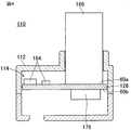
- FIG. 4 is a schematic cross-sectional view of the second embodiment of the wireless LAN module according to the present invention.
- the wireless LAN module 110 illustrated in FIG. 4 includes at least a case 112 and a substrate unit 114.
- the case 112 is provided to accommodate at least the substrate portion 114.
- the case 112 is configured in the same manner as the case 12 in the first embodiment, and thus description thereof is omitted. Further, the description of the substrate projections for supporting the substrate unit 114 is also omitted.
- the substrate unit 114 includes a first substrate 126.
- the first substrate 126 is formed of, for example, a printed board.
- the first substrate 126 is formed in a rectangular plate shape and includes one main surface 60a and the other main surface 60b.
- a first functional block for realizing a predetermined function is arranged on one main surface 60a of the first substrate 126, and has a wiring pattern (not shown) and an electronic component element 164 mounted thereon. Yes. Further, the external connection connector 166 is provided in a region on one end side of the one main surface 60a of the first substrate 126, excluding a region where the electronic component element 64 mounted on the first functional block is mounted. Implemented. As the external connection connector 166, for example, a 5-pin or 8-pin USB connector is used.
- Element 176 is implemented on the other main surface 60b of the first substrate 126, which is a region immediately below the surface on which the external connection connector 166 is mounted.
- the electronic component element 176 is an electronic component element that generates relatively high heat.
- a heat dissipation member may be formed on the surface of the electronic component element 176 opposite to the mounting surface of the first substrate 126. At this time, it is preferable that the surface of the heat radiating member opposite to the surface on which the electronic component element 176 is formed is disposed so as to contact the case 112.
- heat generated in the electronic component element 176 is dissipated as follows. That is, the heat generated in the electronic component element 176 is transferred to the external connection connector 166 through the first substrate 126. The heat transferred to the external connection connector 166 is dissipated through the external connection connector 166 to the electronic device to which the wireless LAN module 110 is connected.
- the heat generated in the electronic component element 176 is transferred to the external connection connector 166 via the first substrate 126, and further, the wireless LAN module 110. Is dissipated to the electronic device to which is connected via the external connector 166. Therefore, the heat generated in the electronic component element 176 can be efficiently radiated.
- FIG. 5 is a schematic sectional view of a wireless LAN module according to a third embodiment of the present invention.
- FIG. 6 (a) is a plan sectional view taken along line AA in FIG. ) Is a plan sectional view taken along line BB in FIG.
- the wireless LAN module 210 further includes a button member 16, a lens member 18, and an antenna 20, which are the same as the button member, the lens member, and the antenna member in the first embodiment. Omitted.
- the case 12 is provided to accommodate at least the substrate part 214.
- the case 12 includes a first case 22 and a second case 24.
- the case 12 is configured in the same manner as the case in the first embodiment, and thus description thereof is omitted. Further, the description of the substrate projections 42 formed on the first case 22 and the substrate projections 58 formed on the second case 24 in the case 12 for supporting the substrate 214 will be omitted.
- the substrate unit 214 includes a first substrate 226 and a second substrate 228.
- the first substrate 226 and the second substrate 228 are formed of, for example, a printed circuit board. Note that the configuration and the like of the first substrate 226 are the same as those of the first substrate 26 of the first embodiment except for the shape of the first substrate 226, and thus the description of the configuration and the like is omitted.
- the configuration of the second substrate 228 is the same as that of the second substrate 28 of the first embodiment except for the shape of the second substrate 228, and thus the description of the configuration and the like is omitted.
- a notch 82 is formed in the substrate.
- the notch 82 may be formed only on the second substrate 228.
- the case 12 becomes hot, so that it is difficult to remove the wireless LAN module 210 from the connected electronic device. Or a problem may occur between the groove 36a in the first case 22 and the protruding edge 52a in the second case 24. This problem is particularly noticeable when the heat capacity of the case 12 is small. For this reason, it is necessary to prevent the heat from being transmitted to the case 12 as much as possible and to transmit the heat to the electronic device side via the external connection connector 66.
- the notch portion 82 is provided by deleting the vicinity of the electronic component element 76a that generates high heat in the first substrate 226 and the second substrate 228. Since the contact between the first substrate 226 and the second substrate 228 and the case 12 can be avoided, heat is hardly transmitted to the case 12, and the above-described problems can be solved.
- FIG. 7A is a schematic cross-sectional view of a wireless LAN module according to a fourth embodiment of the present invention
- FIG. 7B is a cross-sectional plan view taken along the line CC.
- the wireless LAN module 310 illustrated in FIG. 7A includes at least a case 112 and a substrate unit 314.
- the case 112 is provided to accommodate at least the substrate portion 314.
- the case 112 is configured in the same manner as the case 12 in the first embodiment, and thus description thereof is omitted. Further, the description of the substrate protrusion for supporting the substrate portion 314 is also omitted.
- the substrate unit 314 includes a first substrate 326.
- the first substrate 326 is formed by, for example, a printed board. Note that the configuration and the like of the first substrate 326 are the same as those of the first substrate 126 of the second embodiment except for the shape of the first substrate 326, and thus the description of the configuration and the like is omitted.
- a notch portion 382 is formed in the vicinity of the electronic component element 176 that generates high heat in the first substrate 326, as shown in FIG. By forming the notch 382, it is possible to avoid contact between the first substrate 326 and the inner wall surface of the case 112.
- the portion near the electronic component element 176a that generates high heat in the first substrate 326 is deleted and the cutout portion 382 is provided, so that the case 112, the first substrate 326, Therefore, the heat generated from the electronic component element 176a is not easily transmitted to the case 112, like the wireless LAN module 210.
- the case is formed with the board projections to support the board part.
- the invention is not limited to this, and the board part is supported by other configurations. You may make it do. Therefore, the first substrate and the second substrate of the substrate portion in the wireless LAN module according to the above-described embodiment have recesses for penetrating the substrate protrusions on the edge portions. It may not be formed.
- the substrate unit is configured by one or two substrates.
- the substrate unit is not limited to this, and may include three or more substrates. .
- the first functional block is provided on the first board and the second functional block is provided on the second board. It is not a thing.
- the power supply circuit is disposed on the first substrate and the digital circuit is disposed on the second substrate.
- the present invention is not limited to this, and various modifications are made. May be.
- the first substrate is formed thicker than the second substrate.
- the present invention is not limited to this, and the thickness of the first substrate is the second substrate.
- the second substrate may be formed to be thicker than the thickness of the first substrate.
- the composite module according to the present invention can be applied to an application that allows a desired function to be further added to an electronic device such as a home appliance or an AV device.
Landscapes
- Engineering & Computer Science (AREA)
- Microelectronics & Electronic Packaging (AREA)
- Physics & Mathematics (AREA)
- Thermal Sciences (AREA)
- Cooling Or The Like Of Electrical Apparatus (AREA)
- Cooling Or The Like Of Semiconductors Or Solid State Devices (AREA)
- Combinations Of Printed Boards (AREA)
Priority Applications (3)
| Application Number | Priority Date | Filing Date | Title |
|---|---|---|---|
| CN201380025050.9A CN104285292B (zh) | 2012-05-22 | 2013-04-30 | 复合模块 |
| JP2014516737A JP5995015B2 (ja) | 2012-05-22 | 2013-04-30 | 複合モジュール |
| US14/541,286 US9730363B2 (en) | 2012-05-22 | 2014-11-14 | Composite module |
Applications Claiming Priority (4)
| Application Number | Priority Date | Filing Date | Title |
|---|---|---|---|
| JP2012-116983 | 2012-05-22 | ||
| JP2012116983 | 2012-05-22 | ||
| JP2012-205312 | 2012-09-19 | ||
| JP2012205312 | 2012-09-19 |
Related Child Applications (1)
| Application Number | Title | Priority Date | Filing Date |
|---|---|---|---|
| US14/541,286 Continuation US9730363B2 (en) | 2012-05-22 | 2014-11-14 | Composite module |
Publications (1)
| Publication Number | Publication Date |
|---|---|
| WO2013175943A1 true WO2013175943A1 (fr) | 2013-11-28 |
Family
ID=49623641
Family Applications (1)
| Application Number | Title | Priority Date | Filing Date |
|---|---|---|---|
| PCT/JP2013/062522 Ceased WO2013175943A1 (fr) | 2012-05-22 | 2013-04-30 | Module composé |
Country Status (4)
| Country | Link |
|---|---|
| US (1) | US9730363B2 (fr) |
| JP (1) | JP5995015B2 (fr) |
| CN (1) | CN104285292B (fr) |
| WO (1) | WO2013175943A1 (fr) |
Families Citing this family (8)
| Publication number | Priority date | Publication date | Assignee | Title |
|---|---|---|---|---|
| USD954667S1 (en) | 2017-01-13 | 2022-06-14 | Wolfspeed, Inc. | Power module |
| US10212838B2 (en) * | 2017-01-13 | 2019-02-19 | Cree Fayetteville, Inc. | High power multilayer module having low inductance and fast switching for paralleling power devices |
| WO2018216453A1 (fr) * | 2017-05-25 | 2018-11-29 | 株式会社村田製作所 | Dispositif d'antenne |
| FR3068841B1 (fr) * | 2017-07-07 | 2019-08-23 | Alstom Transport Technologies | Dispositif de commutation electrique et coffre de traction electrique associe |
| WO2020043324A1 (fr) | 2018-08-27 | 2020-03-05 | Sew-Eurodrive Gmbh & Co. Kg | Appareil électrique comprenant une partie connexion et une partie couvercle reliée à cette partie connexion |
| USD903590S1 (en) | 2018-09-12 | 2020-12-01 | Cree Fayetteville, Inc. | Power module |
| KR20200132041A (ko) * | 2019-05-15 | 2020-11-25 | 삼성전자주식회사 | 방열 구조를 포함하는 전자 장치 |
| DE112024001813T5 (de) * | 2023-05-23 | 2026-02-26 | The Matias Corporation | Drahtloser nanoempfänger-dongle |
Citations (5)
| Publication number | Priority date | Publication date | Assignee | Title |
|---|---|---|---|---|
| JP2005044904A (ja) * | 2003-07-24 | 2005-02-17 | Murata Mfg Co Ltd | 電子機器 |
| JP2006135202A (ja) * | 2004-11-09 | 2006-05-25 | Yaskawa Electric Corp | 電子機器の放熱構造 |
| JP2007299338A (ja) * | 2006-05-08 | 2007-11-15 | Matsushita Electric Ind Co Ltd | カード型情報装置 |
| JP2010211157A (ja) * | 2009-03-12 | 2010-09-24 | Hitachi Cable Ltd | 光送受信器 |
| JP2012094695A (ja) * | 2010-10-27 | 2012-05-17 | Kyocera Corp | 携帯情報端末 |
Family Cites Families (10)
| Publication number | Priority date | Publication date | Assignee | Title |
|---|---|---|---|---|
| US7407390B1 (en) * | 2005-05-16 | 2008-08-05 | Super Talent Electronics, Inc. | USB device with plastic housing having inserted plug support |
| US7382625B2 (en) * | 2006-01-23 | 2008-06-03 | Sony Ericsson Mobile Communications Ab | Combination antenna and SIM card support structure |
| US8018734B2 (en) * | 2007-08-24 | 2011-09-13 | Novatel Wireless, Inc. | Electronic device and method of forming same |
| CN101909415A (zh) * | 2009-06-02 | 2010-12-08 | 鸿富锦精密工业(深圳)有限公司 | 散热装置及其固定支架 |
| TWI381268B (zh) * | 2009-12-04 | 2013-01-01 | Wistron Neweb Corp | 通用序列匯流排裝置 |
| EP2355628B1 (fr) * | 2010-01-29 | 2013-10-16 | LG Electronics Inc. | Terminal mobile |
| JP5568332B2 (ja) | 2010-02-22 | 2014-08-06 | 日本圧着端子製造株式会社 | 電気コネクタ |
| JP2011198951A (ja) | 2010-03-18 | 2011-10-06 | Fujitsu Ten Ltd | 制御装置 |
| KR101788599B1 (ko) * | 2010-09-10 | 2017-10-20 | 엘지전자 주식회사 | 동글장치 |
| US20120129481A1 (en) * | 2010-11-18 | 2012-05-24 | Bandrich, Inc. | Wireless network receiver |
-
2013
- 2013-04-30 WO PCT/JP2013/062522 patent/WO2013175943A1/fr not_active Ceased
- 2013-04-30 JP JP2014516737A patent/JP5995015B2/ja not_active Expired - Fee Related
- 2013-04-30 CN CN201380025050.9A patent/CN104285292B/zh not_active Expired - Fee Related
-
2014
- 2014-11-14 US US14/541,286 patent/US9730363B2/en not_active Expired - Fee Related
Patent Citations (5)
| Publication number | Priority date | Publication date | Assignee | Title |
|---|---|---|---|---|
| JP2005044904A (ja) * | 2003-07-24 | 2005-02-17 | Murata Mfg Co Ltd | 電子機器 |
| JP2006135202A (ja) * | 2004-11-09 | 2006-05-25 | Yaskawa Electric Corp | 電子機器の放熱構造 |
| JP2007299338A (ja) * | 2006-05-08 | 2007-11-15 | Matsushita Electric Ind Co Ltd | カード型情報装置 |
| JP2010211157A (ja) * | 2009-03-12 | 2010-09-24 | Hitachi Cable Ltd | 光送受信器 |
| JP2012094695A (ja) * | 2010-10-27 | 2012-05-17 | Kyocera Corp | 携帯情報端末 |
Also Published As
| Publication number | Publication date |
|---|---|
| JP5995015B2 (ja) | 2016-09-21 |
| CN104285292A (zh) | 2015-01-14 |
| US20150124409A1 (en) | 2015-05-07 |
| US9730363B2 (en) | 2017-08-08 |
| JPWO2013175943A1 (ja) | 2016-01-12 |
| CN104285292B (zh) | 2017-12-19 |
Similar Documents
| Publication | Publication Date | Title |
|---|---|---|
| JP5995015B2 (ja) | 複合モジュール | |
| JP5811278B2 (ja) | 複合モジュール | |
| JP6520568B2 (ja) | アンテナ装置 | |
| KR102537318B1 (ko) | 회로 기판 어셈블리 및 그것을 포함하는 전자 장치 | |
| US10090596B2 (en) | Robust antenna configurations for wireless connectivity of smart home devices | |
| JP5522066B2 (ja) | 光通信用カードモジュール | |
| JP6000337B2 (ja) | 撮像装置 | |
| CN202956504U (zh) | 内置模块的连接器 | |
| EP3525235A1 (fr) | Module de communication et sa structure de montage | |
| JP2012231386A (ja) | アンテナ、及び通信装置 | |
| US20070134003A1 (en) | Optical transceiver case | |
| WO2013175942A1 (fr) | Module composé | |
| JP2008227653A (ja) | 撮像素子を有する半導体装置 | |
| US10072833B2 (en) | Light apparatus with control board thermally insulated from light source | |
| JP2013201233A (ja) | 電源装置 | |
| KR20220076083A (ko) | 노이즈 유도 구조를 포함하는 전자 장치 | |
| KR102717135B1 (ko) | Mid와 mdm을 적용한 열전도 패드가 구비된 전자기기 및 그 제조방법 | |
| CN211352620U (zh) | 功率变换器的布局结构 | |
| JP2020053567A (ja) | 光モジュール | |
| WO2014061306A1 (fr) | Module composite | |
| KR20190035068A (ko) | 케이스 및 이를 구비한 무선전력송신기 | |
| JP2011159867A (ja) | 筐体及び基地局 | |
| KR101922381B1 (ko) | 방열 부재를 포함하는 플렉시블 인쇄회로기판 제조 방법 | |
| KR102059816B1 (ko) | 통신 모듈 및 그 실장 구조 | |
| KR101922380B1 (ko) | 방열 부재를 포함하는 플렉시블 인쇄회로기판 |
Legal Events
| Date | Code | Title | Description |
|---|---|---|---|
| 121 | Ep: the epo has been informed by wipo that ep was designated in this application |
Ref document number: 13794307 Country of ref document: EP Kind code of ref document: A1 |
|
| ENP | Entry into the national phase |
Ref document number: 2014516737 Country of ref document: JP Kind code of ref document: A |
|
| NENP | Non-entry into the national phase |
Ref country code: DE |
|
| 122 | Ep: pct application non-entry in european phase |
Ref document number: 13794307 Country of ref document: EP Kind code of ref document: A1 |