WO2013176077A1 - Appareil de conception lsi, procédé de conception lsi et programme - Google Patents
Appareil de conception lsi, procédé de conception lsi et programme Download PDFInfo
- Publication number
- WO2013176077A1 WO2013176077A1 PCT/JP2013/063914 JP2013063914W WO2013176077A1 WO 2013176077 A1 WO2013176077 A1 WO 2013176077A1 JP 2013063914 W JP2013063914 W JP 2013063914W WO 2013176077 A1 WO2013176077 A1 WO 2013176077A1
- Authority
- WO
- WIPO (PCT)
- Prior art keywords
- selector
- input
- output flow
- module
- macro
- Prior art date
- Legal status (The legal status is an assumption and is not a legal conclusion. Google has not performed a legal analysis and makes no representation as to the accuracy of the status listed.)
- Ceased
Links
Images



Classifications
-
- G—PHYSICS
- G06—COMPUTING OR CALCULATING; COUNTING
- G06F—ELECTRIC DIGITAL DATA PROCESSING
- G06F30/00—Computer-aided design [CAD]
- G06F30/30—Circuit design
- G06F30/32—Circuit design at the digital level
- G06F30/327—Logic synthesis; Behaviour synthesis, e.g. mapping logic, HDL to netlist, high-level language to RTL or netlist
-
- G—PHYSICS
- G06—COMPUTING OR CALCULATING; COUNTING
- G06F—ELECTRIC DIGITAL DATA PROCESSING
- G06F30/00—Computer-aided design [CAD]
- G06F30/30—Circuit design
- G06F30/39—Circuit design at the physical level
- G06F30/394—Routing
-
- G—PHYSICS
- G06—COMPUTING OR CALCULATING; COUNTING
- G06F—ELECTRIC DIGITAL DATA PROCESSING
- G06F2115/00—Details relating to the type of the circuit
- G06F2115/08—Intellectual property [IP] blocks or IP cores
Definitions
- the present invention relates to the design of an LSI (Large Scale Integrated Circuit).
- IP Intelligent Property
- a system LSI for video signal processing is taken as an example. If there is a request to support two systems of input / output with different resolutions and image formats on a single chip, each system should have exactly the same video signal processing function to configure an LSI in which the two systems operate independently. The required function can be satisfied. However, such an implementation does not actually implement such an implementation because the circuit scale becomes enormous.
- an LSI use case is defined as a restriction item, and an LSI use case is defined as an operation mode. If there are a plurality of functions that do not operate simultaneously in a certain mode, the plurality of functions are merged to perform optimization so that the plurality of functions can be realized with a minimum number of IPs.
- the present invention has been made in view of the above points, and its main object is to improve design efficiency when designing an LSI.
- An LSI design apparatus includes: Input / output flow information describing the input / output flow of signals between functional blocks included in the LSI (Large Scale Integrated Circuit) to be designed is input, the input / output flow information is analyzed, and described in the input / output flow information
- a selector module generation unit that generates a selector module of a selector that matches the input / output flow of signals between functional blocks that are It has a macro module generation part which generates a macro module showing a relation between a selector and a functional block using a selector module generated by the selector module generation part.
- a selector module of a selector that analyzes input / output flow information and matches a signal input / output flow between functional blocks described in the input / output flow information, a macroblock including the selector module, and a selector Since the CPU bus IF for controlling the module is automatically generated, the design efficiency when designing the LSI can be improved.
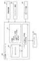
- FIG. 3 is a diagram showing a configuration example of an LSI design platform according to the first embodiment.
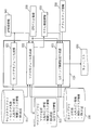
- 1 is a diagram illustrating a configuration example of a system LSI assembly device according to Embodiment 1.
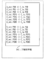
- FIG. 4 shows an example of IP connection information according to the first embodiment.
- FIG. 4 shows an example of IP connection information according to the first embodiment.
- FIG. 3 is a diagram illustrating an example of a selector module according to the first embodiment.
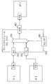
- FIG. 3 is a diagram illustrating an example of a macro module according to the first embodiment.
- FIG. 4 is a diagram illustrating an example of control register information according to the first embodiment.
- FIG. 6 is a diagram showing an example of generating macro connection information according to the first embodiment.
- FIG. 5 is a diagram showing an example of address map information according to the first embodiment.
- FIG. 3 is a diagram illustrating an example of a net list according to the first embodiment.
- FIG. 3 is a diagram illustrating a hardware configuration example of a system LSI assembly device according to the first embodiment.
- Embodiment 1 a system LSI design platform that constitutes a system LSI by interconnecting a plurality of functional blocks including IP will be described.
- the system LSI design platform according to the present embodiment includes a selector module generation unit, a macro module generation unit, and an LSI top connection description generation unit.
- the selector module generation unit generates a selector module necessary for configuring a connection relationship between a plurality of functional blocks including IP.
- the macro module generation unit generates a macro module including a selector module generated by the selector module generation unit and an IP connected to the selector module.
- the LSI top connection description generation unit interconnects the macro module generated by the macro module generation unit and the IP to generate an LSI top description.
- the design efficiency is improved because a new selector design and a design change of the CPU bus IF that are necessary for each system LSI design are automated.
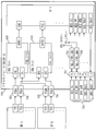
- FIG. 1 is a block diagram showing a configuration example of a system LSI design platform according to the present embodiment.
- the LSI design platform 000 includes an IP library 100 and a system LSI assembly device 020.
- the system LSI assembly device 020 receives the IP connection information 040, the address map information 200, and the CPU bus IF information 300, and outputs a net list 030.
- the netlist 030 is a connection description of the system LSI top described in HDL (Hardware Description Language). Details of the IP connection information 040, the address map information 200, and the CPU bus IF information 300 will be described later.
- the IP library 100 includes IP information 101 regarding each IP included in the library, and the IP information 101 includes, for example, an IP name, input / output pin information, control register information, and HDL description.
- the IP library 100 includes IP information 101 regarding IP included in the system LSI to be designed.
- the system LSI assembly device 020 corresponds to an example of an LSI design device.
- the system LSI assembly device 020 includes a selector module generation unit 021, a macro module generation unit 022, and an LSI top connection description generation unit 023 inside.
- the selector module generation unit 021 receives the IP connection information 040 and generates a selector library 011.
- the selector library 011 information on the selector module generated by the selector module generation unit 021 is described.
- the selector library 011 includes, for example, an IP name (selector name), input / output pin information, control register information, and HDL description.
- the selector module is a functional block 060 in which a selector 064, input pins 061, 062, an output pin 063, and a selector control signal input interface 065 are associated with each other, as shown in FIG.
- the input pins 061 and 062 are pins for the selector 064 to input a signal from the IP.
- the output pin 063 is a pin for the selector 064 to output a signal to the IP.
- the selector control signal input interface 065 is an interface for inputting a control signal. Note that “generate a selector module” means that a template of the selector module 060 as shown in FIG. 5 is generated.
- the detailed information of the template is information of the selector library 011 (IP name (selector name), input / output pin information, control register information, HDL description).
- IP name vector name
- the selector module generation unit 021 when a 2to1 selector is required, the selector module generation unit 021 generates a selector module template of a 2to1 selector as shown in FIG.
- the selector module generation unit 021 When a 3to1 selector is necessary, the selector module generation unit 021 generates a selector module template of the 3to1 selector corresponding to the configuration of FIG.
- the selector module generation unit 021 registers the detailed information of the generated template in the selector library 011.
- the macro module generation unit 022 described later generates, for example, an instance of the selector module of the 2to1 selector using the information of the selector library 011 and also generates an instance of the selector module of the 3to1 selector.
- the IP connection information 040 represents, for example, a connection relationship between IPs in a specific format (excluding the CPU bus IF) as shown in an IP connection information example 041 in FIG.
- the IP connection information example 041 in FIG. 3 represents the connection relationship for three of IP A, B, and C.
- A_out, B_out, and C_in are keywords representing the IP A output signal, the IP B output signal, and the IP C input signal, respectively.
- PXR represents the PXR signal (output) of IP A.
- PXR > C_in.
- IP connection information example 041 indicates that the IP A PXR signal (output) is connected to the IP C PXR signal (input).
- the description format of the IP connection information 040 is not limited. As shown in FIG. 3, the IP connection information 040 is information describing an input / output flow of signals between functional blocks included in the LSI to be designed, and corresponds to an example of input / output flow information.
- the selector module generation unit 021 scans the IP connection information 040 and checks whether it is necessary to insert a selector for each input signal. When it is necessary to insert a selector, the selector module generation unit 021 generates a selector module. Whether or not selector insertion is necessary is determined by checking whether or not a plurality of output signals are connected to one input signal. For example, in the example of the IP connection information example 041 (FIG. 3), the input signal C_in. For PXR, the output signal A_out. PXR and output signal B_out. PXR is connected. For this reason, the input signal C_in. A 2 to 1 selector insertion is required before PXR input.
- the selector module generation unit 021 generates a selector module of a 2to1 selector. As described above, the selector module generation unit 021 analyzes the IP connection information 040 and generates a selector module of a selector that matches the input / output flow of signals between IPs described in the IP connection information 040.
- FIG. 5 shows an example of the selector module 060 generated by the selector module generation unit 021.
- the selector module 060 includes input pins 061 and 062, an output pin 063, and a selector control signal interface 065.
- the input pins 061 and 062 are pins for the 2to1 selector 064 to input signals from IP A and IP B.
- the output pin 063 is a pin for the 2to1 selector 064 to output a signal to the IPC.
- the selector control signal input interface 065 is an interface for controlling the 2to1 selector 064.
- NtoM N and M are natural numbers and N ⁇ M).
- the selector module generation unit 021 analyzes the IP connection information 040 and associates two or more IPs, each of which inputs / outputs the same type of signal (PXR signal, PXG signal, etc.).
- the selector module generation unit 021 has input pins corresponding to the number (N) of IPs that output signals among the associated IPs, and the number (M) of IPs that input signals among the associated IPs.
- a selector module of an NtoM selector having a minute output pin is generated. The above generation is repeatedly performed to generate all necessary selector modules, and then information on the generated selector modules is output as a selector library 011.
- the selector library 011 already includes a selector module having the same function, for example, a 2to1 selector, it is not duplicated.
- the macro module generation unit 022 generates a macro module with the IP information 101 of the IP library 100, the CPU bus IF information 300, the selector library 011 output from the selector module generation unit 021 and the IP connection information 040 as inputs. Then, the macro module generation unit 022 outputs the generated macro module as a macro library 012.
- the macro module generated here is a wrapper module including the selector module generated by the selector module generation unit 021 and the IP to which the output of the selector module is connected.
- the macro library 012 includes, for example, macro name, input / output pin information, control register information, HDL description, and included IP information.
- FIG. 6 shows a macro module 700 generated in the case of the IP connection information 041 shown in FIG.
- the macro module generation unit 022 scans the IP connection information 040 (041), and checks the IP input signal into which the selector is inserted. When there is an input signal that requires insertion of a selector, the macro module generation unit 022 selects a selector module having a function necessary for configuring a connection relationship from the selector library 011. In this case, the macro module generation unit 022 selects the 2to1 selector module 060 (FIG. 5). Then, the macro module generation unit 022 connects the selector module 600 that is an instance of the selector module 060 and the IPC in the macro module 700.
- the macro module generation unit 022 generates new macro module input ports 701 and 702 connected to the selector input, and simultaneously generates a control register 703 for the selector. Further, the macro module generation unit 022 adds a register selector 751 to the control register 703 so that the CPU bus IF 750 can read / write based on the CPU bus IF information 300. Further, the macro module generation unit 022 reads IP C control register information included in the macro module from the IP library 100. The macro module generation unit 022 adds the information of the control register 703 to the read IP C control register information to generate the macro module control register information.
- the CPU bus IF information 300 is information that associates the signal name of the CPU bus IF with the meaning of the signal.
- the CPU bus IF information 300 includes a chip select signal (BUS CS), a read / write control signal (BUS RW), an address signal (BUS ADR), a write data signal (BUS WDAT), and a read data signal (BUS).
- RDAT corresponds to the actual CPU bus IF.
- the control register information is information in which a correspondence between a control register included in the IP and a bus address is described in a specific format.
- the control register information is information in which an address (0000, etc.) and a control register name (control register 0, etc.) are associated with each other with a blank as shown by a reference numeral 601 in FIG.
- the first line of FIG. 7 indicates that if the bus address (FIG. 6 BUS ADR) 0000h is input when the bus IF chip select (FIG. 6 BUC CS signal) is valid, the control register 0 in the IP can be accessed. Represents. The same contents are described for the second and subsequent lines.
- the macro module generation unit 022 rewrites the corresponding part of the IP connection information 040 (041) to information indicating the connection with the macro module at the part where the IP is connected in the macro module, and the macro connection information 050 (051). Is generated (FIG. 8).
- the row of reference numeral 402 in the IP connection information 041 is rewritten as the row of reference numeral 502.
- the line 403 is rewritten as the line 503.
- the macro connection information 051 is generated.
- the corresponding line in the IP connection information 041 is rewritten in the format shown in FIG.
- the macro module generation unit 022 In the IP connection information 041 shown in FIG. 3, it is necessary to insert a 2to1 selector for other types of signals such as PXG and PXB. For this reason, the macro module generation unit 022 generates an instance of a 2to1 selector module (FIG. 5) for each signal. The macro module generation unit 022 connects each selector module and the IPC in the macro module 700. Further, the macro module generation unit 022 generates a macro module input port and rewrites the IP connection information 040 for each signal. The macro module generation unit 022 continues these processes until generation of the macro module becomes unnecessary, generates all macro modules, and outputs the macro library 012. In FIG.
- control register information shown in FIG. 7 is used to simplify the description, and does not limit the format for expressing the control register information.
- the LSI top connection description generation unit 023 inputs the macro library 012, the macro connection information 050, and the address map information 200 generated by the macro module generation unit 022, and generates a final netlist 030.
- the address map information 200 is a file described in a specific format.
- the address map information 200 indicates which address on the system is mapped to the head of which control register of which IP.
- the control register of IP A is mapped to the system address 1500_0000h and later.
- mapping of the IP B control register to the system address 1500 — 0100h and later is shown.
- IP C control register is mapped to the system address 1500_0200 and thereafter.
- the address / IP name pair is described in a line with a space between each line, but this is an example used for simplifying the description. There is no limit.
- the LSI top connection description generation unit 023 generates an IP and macro module connection description according to the macro connection information 050.
- the LSI top connection description generation unit 023 generates an address decoder 310 that outputs a chip select signal (FIG. 6 BUS CS signal) in the CPU bus IF according to the address map information 200 (FIG. 10).
- the LSI top connection description generation unit 023 connects the generated chip select signal of the address decoder 310 to the IP chip select signal described in the address map information 200.
- the IP name of the IP included in the macro module does not exist in the macro connection information 050.
- the LSI top connection description generating unit 023 checks the IP information included in the macro library 012 and connects the chip select signal of the address decoder 310 to the chip select input of the macro module including the corresponding IP. Finally, the LSI top connection description generation unit 023 connects the CPU bus IF portions based on the CPU bus IF information 300.
- a system LSI design platform has been described in which a system LSI is configured by interconnecting a plurality of functional blocks including IP (Intellectual Property).
- IP IP
- a selector module generation unit that generates a selector module necessary for configuring a connection relationship between a plurality of functional blocks including IP
- a macro module generation unit that generates a macro module including a selector module generated by the selector module generation unit and an IP connected to the selector module
- the system LSI design platform including the LSI top connection description generation unit that generates the top description of the LSI by interconnecting the macro module generated by the macro module and the IP has been described.
- the macro module generation unit generates a macro module including a selector module generated by the selector module generation unit and an IP to which an output of the selector module is connected, from IP connection information representing a connection relationship between a plurality of functional blocks including IP.
- the macro module generation unit described above generates the CPU bus IF in the macro module IF for accessing the selector module generated by the selector module generation unit and the control register included in the IP based on the CPU bus IF information. .
- the LSI top connection description generation unit generates an address decoder necessary for accessing from the CPU bus IF to the control register in the macro module generated by the IP and the macro module generation unit based on the address map information. It has been explained that the decoder is connected to the CPU bus IF of the IP and macro module.
- the system LSI assembly device 020 is a computer, and each element of the system LSI assembly device 020 can be realized by a program.
- an arithmetic device 901, an external storage device 902, a main storage device 903, a communication device 904, and an input / output device 905 are connected to the bus.
- the arithmetic device 901 is a CPU that executes a program.
- the external storage device 902 is, for example, a ROM (Read Only Memory), a flash memory, or a hard disk device.
- the main storage device 903 is a RAM (Random Access Memory).
- the communication device 904 is a communication card, for example.
- the input / output device 905 is, for example, a mouse, a keyboard, a display device, or the like. The input / output device 905 receives, for example, the IP connection information 040, the address map information 200, and the CPU bus IF information 300, and displays the net list 030.
- the program is normally stored in the external storage device 902, and is loaded into the main storage device 903 and sequentially read into the arithmetic device 901 and executed.
- the program is a program that realizes the functions described as “unit” shown in FIG.
- an operating system (OS) is also stored in the external storage device 902.
- OS operating system
- At least a part of the OS is loaded into the main storage device 903, and the arithmetic device 901 executes “OS” shown in FIG. ”Is executed.
- the input IP connection information 040, address map information 200, and CPU bus IF information 300 are also sequentially loaded into the main storage device 903 and used by the arithmetic unit 901.
- Information on the generated selector library 011 and macro library 012 is also stored in the main storage device 903 and used by the arithmetic unit 901.
- FIG. 11 is merely an example of the hardware configuration of the system LSI assembly device 020, and the hardware configuration of the system LSI assembly device 020 is not limited to the configuration illustrated in FIG. There may be.
- the LSI design method according to the present invention can be realized by the procedure shown in the present embodiment.
Landscapes
- Engineering & Computer Science (AREA)
- Computer Hardware Design (AREA)
- Physics & Mathematics (AREA)
- Theoretical Computer Science (AREA)
- Evolutionary Computation (AREA)
- Geometry (AREA)
- General Engineering & Computer Science (AREA)
- General Physics & Mathematics (AREA)
- Computer Networks & Wireless Communication (AREA)
- Design And Manufacture Of Integrated Circuits (AREA)
Abstract
Priority Applications (2)
| Application Number | Priority Date | Filing Date | Title |
|---|---|---|---|
| US14/380,447 US9122831B2 (en) | 2012-05-21 | 2013-05-20 | LSI designing apparatus, LSI designing method, and program |
| JP2014516788A JP5791797B2 (ja) | 2012-05-21 | 2013-05-20 | Lsi設計装置及びlsi設計方法及びプログラム |
Applications Claiming Priority (2)
| Application Number | Priority Date | Filing Date | Title |
|---|---|---|---|
| JP2012115508 | 2012-05-21 | ||
| JP2012-115508 | 2012-05-21 |
Publications (1)
| Publication Number | Publication Date |
|---|---|
| WO2013176077A1 true WO2013176077A1 (fr) | 2013-11-28 |
Family
ID=49623767
Family Applications (1)
| Application Number | Title | Priority Date | Filing Date |
|---|---|---|---|
| PCT/JP2013/063914 Ceased WO2013176077A1 (fr) | 2012-05-21 | 2013-05-20 | Appareil de conception lsi, procédé de conception lsi et programme |
Country Status (3)
| Country | Link |
|---|---|
| US (1) | US9122831B2 (fr) |
| JP (1) | JP5791797B2 (fr) |
| WO (1) | WO2013176077A1 (fr) |
Families Citing this family (1)
| Publication number | Priority date | Publication date | Assignee | Title |
|---|---|---|---|---|
| US12430474B1 (en) * | 2022-08-31 | 2025-09-30 | Cadence Design Systems, Inc. | Locking mechanism and core wrapping for IP core |
Citations (3)
| Publication number | Priority date | Publication date | Assignee | Title |
|---|---|---|---|---|
| JP2004213301A (ja) * | 2002-12-27 | 2004-07-29 | Renesas Technology Corp | 自動回路設計装置およびプログラム |
| JP2006244274A (ja) * | 2005-03-04 | 2006-09-14 | Matsushita Electric Ind Co Ltd | Lsi設計方法 |
| JP2007193842A (ja) * | 2007-04-09 | 2007-08-02 | Matsushita Electric Ind Co Ltd | Ipベースlsi設計システムおよび設計方法 |
Family Cites Families (10)
| Publication number | Priority date | Publication date | Assignee | Title |
|---|---|---|---|---|
| JP3974300B2 (ja) | 1999-11-18 | 2007-09-12 | 松下電器産業株式会社 | Ipベースlsi設計システムおよび設計方法 |
| US6993740B1 (en) * | 2000-04-03 | 2006-01-31 | International Business Machines Corporation | Methods and arrangements for automatically interconnecting cores in systems-on-chip |
| JP3852741B2 (ja) | 2000-10-31 | 2006-12-06 | シャープ株式会社 | 高位合成方法および高位合成装置 |
| JP2002342259A (ja) | 2001-05-21 | 2002-11-29 | Hitachi Ltd | Dmaコントローラおよびdmaコントローラ自動生成装置 |
| US6973631B2 (en) * | 2002-07-18 | 2005-12-06 | Incentia Design Systems Corp. | Scan insertion with bypass login in an IC design |
| JP4390639B2 (ja) | 2004-06-21 | 2009-12-24 | Necエレクトロニクス株式会社 | Lsi設計システム、lsi設計プログラム |
| JP2006065457A (ja) | 2004-08-25 | 2006-03-09 | Fuji Xerox Co Ltd | インタフェース回路生成装置およびインタフェース回路 |
| US8413106B1 (en) * | 2004-10-28 | 2013-04-02 | Synopsys, Inc. | Transaction level model synthesis |
| US7966529B2 (en) * | 2006-10-16 | 2011-06-21 | Freescale Semiconductor, Inc. | System and method for testing memory blocks in an SOC design |
| JP5632651B2 (ja) | 2010-05-19 | 2014-11-26 | スパンション エルエルシー | 半導体回路及び設計装置 |
-
2013
- 2013-05-20 JP JP2014516788A patent/JP5791797B2/ja not_active Expired - Fee Related
- 2013-05-20 US US14/380,447 patent/US9122831B2/en not_active Expired - Fee Related
- 2013-05-20 WO PCT/JP2013/063914 patent/WO2013176077A1/fr not_active Ceased
Patent Citations (3)
| Publication number | Priority date | Publication date | Assignee | Title |
|---|---|---|---|---|
| JP2004213301A (ja) * | 2002-12-27 | 2004-07-29 | Renesas Technology Corp | 自動回路設計装置およびプログラム |
| JP2006244274A (ja) * | 2005-03-04 | 2006-09-14 | Matsushita Electric Ind Co Ltd | Lsi設計方法 |
| JP2007193842A (ja) * | 2007-04-09 | 2007-08-02 | Matsushita Electric Ind Co Ltd | Ipベースlsi設計システムおよび設計方法 |
Also Published As
| Publication number | Publication date |
|---|---|
| JPWO2013176077A1 (ja) | 2016-01-14 |
| US20150033200A1 (en) | 2015-01-29 |
| US9122831B2 (en) | 2015-09-01 |
| JP5791797B2 (ja) | 2015-10-07 |
Similar Documents
| Publication | Publication Date | Title |
|---|---|---|
| US8959472B1 (en) | Considering compatibility of adjacent boundary regions for standard cells placement and routing | |
| US8997033B1 (en) | Techniques for generating a single configuration file for multiple partial reconfiguration regions | |
| US11726545B2 (en) | Methods and apparatus for selectively extracting and loading register states | |
| US20070283311A1 (en) | Method and system for dynamic reconfiguration of field programmable gate arrays | |
| US9298865B1 (en) | Debugging an optimized design implemented in a device with a pre-optimized design simulation | |
| US11675613B2 (en) | Flexible physical function and virtual function mapping | |
| US9864828B1 (en) | Hardware acceleration device handoff for using programmable integrated circuits as hardware accelerators | |
| CN102857213A (zh) | 可重构逻辑块 | |
| US10437946B1 (en) | Using implemented core sources for simulation | |
| JP2021534471A (ja) | 回路配線記憶方法、fpgaシステムおよび記憶媒体 | |
| JP5791797B2 (ja) | Lsi設計装置及びlsi設計方法及びプログラム | |
| US10152566B1 (en) | Constraint based bit-stream compression in hardware for programmable devices | |
| US20240126960A1 (en) | Intelligent Suggestions for CAD-Based Design Entry | |
| WO2014042190A1 (fr) | Dispositif à logique programmable et procédé de validation | |
| CN110414029B (zh) | 半导体lsi设计装置以及设计方法 | |
| KR20070097051A (ko) | 동적으로 재구성 가능한 프로세서 | |
| Charaf et al. | Amah-flex: A modular and highly flexible tool for generating relocatable systems on fpgas | |
| US10372946B1 (en) | Systems and methods for configuring a secure computing environment on an integrated circuit | |
| JP6638362B2 (ja) | 演算処理装置、演算処理システムおよび演算処理方法 | |
| JPWO2006025412A1 (ja) | 論理検証方法、論理モジュールデータ、デバイスデータおよび論理検証装置 | |
| US8539415B2 (en) | Reconfigurable circuit, its design method, and design apparatus | |
| JP2016139203A (ja) | 設計情報作成方法、設計情報作成装置及びプログラム | |
| CN120597801A (zh) | 一种在线编辑fpga内存的方法及装置 | |
| Jantsch | Modeling and Design Flow Basics | |
| CN120579505A (zh) | 一种数据流获取方法、装置、设备及介质 |
Legal Events
| Date | Code | Title | Description |
|---|---|---|---|
| 121 | Ep: the epo has been informed by wipo that ep was designated in this application |
Ref document number: 13793371 Country of ref document: EP Kind code of ref document: A1 |
|
| ENP | Entry into the national phase |
Ref document number: 2014516788 Country of ref document: JP Kind code of ref document: A |
|
| WWE | Wipo information: entry into national phase |
Ref document number: 14380447 Country of ref document: US |
|
| NENP | Non-entry into the national phase |
Ref country code: DE |
|
| 122 | Ep: pct application non-entry in european phase |
Ref document number: 13793371 Country of ref document: EP Kind code of ref document: A1 |