WO2013179879A1 - Module semi-conducteur et procédé de fabrication d'un module semi-conducteur - Google Patents
Module semi-conducteur et procédé de fabrication d'un module semi-conducteur Download PDFInfo
- Publication number
- WO2013179879A1 WO2013179879A1 PCT/JP2013/063290 JP2013063290W WO2013179879A1 WO 2013179879 A1 WO2013179879 A1 WO 2013179879A1 JP 2013063290 W JP2013063290 W JP 2013063290W WO 2013179879 A1 WO2013179879 A1 WO 2013179879A1
- Authority
- WO
- WIPO (PCT)
- Prior art keywords
- region
- frame
- semiconductor module
- frame body
- wiring board
- Prior art date
- Legal status (The legal status is an assumption and is not a legal conclusion. Google has not performed a legal analysis and makes no representation as to the accuracy of the status listed.)
- Ceased
Links
Images

Classifications
-
- H—ELECTRICITY
- H10—SEMICONDUCTOR DEVICES; ELECTRIC SOLID-STATE DEVICES NOT OTHERWISE PROVIDED FOR
- H10W—GENERIC PACKAGES, INTERCONNECTIONS, CONNECTORS OR OTHER CONSTRUCTIONAL DETAILS OF DEVICES COVERED BY CLASS H10
- H10W72/00—Interconnections or connectors in packages
-
- H—ELECTRICITY
- H10—SEMICONDUCTOR DEVICES; ELECTRIC SOLID-STATE DEVICES NOT OTHERWISE PROVIDED FOR
- H10W—GENERIC PACKAGES, INTERCONNECTIONS, CONNECTORS OR OTHER CONSTRUCTIONAL DETAILS OF DEVICES COVERED BY CLASS H10
- H10W76/00—Containers; Fillings or auxiliary members therefor; Seals
- H10W76/10—Containers or parts thereof
- H10W76/12—Containers or parts thereof characterised by their shape
- H10W76/15—Containers comprising an insulating or insulated base
-
- H—ELECTRICITY
- H10—SEMICONDUCTOR DEVICES; ELECTRIC SOLID-STATE DEVICES NOT OTHERWISE PROVIDED FOR
- H10W—GENERIC PACKAGES, INTERCONNECTIONS, CONNECTORS OR OTHER CONSTRUCTIONAL DETAILS OF DEVICES COVERED BY CLASS H10
- H10W90/00—Package configurations
-
- H—ELECTRICITY
- H10—SEMICONDUCTOR DEVICES; ELECTRIC SOLID-STATE DEVICES NOT OTHERWISE PROVIDED FOR
- H10W—GENERIC PACKAGES, INTERCONNECTIONS, CONNECTORS OR OTHER CONSTRUCTIONAL DETAILS OF DEVICES COVERED BY CLASS H10
- H10W40/00—Arrangements for thermal protection or thermal control
- H10W40/20—Arrangements for cooling
- H10W40/25—Arrangements for cooling characterised by their materials
-
- H—ELECTRICITY
- H10—SEMICONDUCTOR DEVICES; ELECTRIC SOLID-STATE DEVICES NOT OTHERWISE PROVIDED FOR
- H10W—GENERIC PACKAGES, INTERCONNECTIONS, CONNECTORS OR OTHER CONSTRUCTIONAL DETAILS OF DEVICES COVERED BY CLASS H10
- H10W40/00—Arrangements for thermal protection or thermal control
- H10W40/60—Securing means for detachable heating or cooling arrangements, e.g. clamps
- H10W40/611—Bolts or screws
-
- H—ELECTRICITY
- H10—SEMICONDUCTOR DEVICES; ELECTRIC SOLID-STATE DEVICES NOT OTHERWISE PROVIDED FOR
- H10W—GENERIC PACKAGES, INTERCONNECTIONS, CONNECTORS OR OTHER CONSTRUCTIONAL DETAILS OF DEVICES COVERED BY CLASS H10
- H10W72/00—Interconnections or connectors in packages
- H10W72/071—Connecting or disconnecting
- H10W72/075—Connecting or disconnecting of bond wires
-
- H—ELECTRICITY
- H10—SEMICONDUCTOR DEVICES; ELECTRIC SOLID-STATE DEVICES NOT OTHERWISE PROVIDED FOR
- H10W—GENERIC PACKAGES, INTERCONNECTIONS, CONNECTORS OR OTHER CONSTRUCTIONAL DETAILS OF DEVICES COVERED BY CLASS H10
- H10W72/00—Interconnections or connectors in packages
- H10W72/50—Bond wires
- H10W72/541—Dispositions of bond wires
- H10W72/5445—Dispositions of bond wires being orthogonal to a side surface of the chip, e.g. parallel arrangements
-
- H—ELECTRICITY
- H10—SEMICONDUCTOR DEVICES; ELECTRIC SOLID-STATE DEVICES NOT OTHERWISE PROVIDED FOR
- H10W—GENERIC PACKAGES, INTERCONNECTIONS, CONNECTORS OR OTHER CONSTRUCTIONAL DETAILS OF DEVICES COVERED BY CLASS H10
- H10W72/00—Interconnections or connectors in packages
- H10W72/50—Bond wires
- H10W72/541—Dispositions of bond wires
- H10W72/547—Dispositions of multiple bond wires
- H10W72/5475—Dispositions of multiple bond wires multiple bond wires connected to common bond pads at both ends of the wires
-
- H—ELECTRICITY
- H10—SEMICONDUCTOR DEVICES; ELECTRIC SOLID-STATE DEVICES NOT OTHERWISE PROVIDED FOR
- H10W—GENERIC PACKAGES, INTERCONNECTIONS, CONNECTORS OR OTHER CONSTRUCTIONAL DETAILS OF DEVICES COVERED BY CLASS H10
- H10W72/00—Interconnections or connectors in packages
- H10W72/851—Dispositions of multiple connectors or interconnections
- H10W72/874—On different surfaces
- H10W72/884—Die-attach connectors and bond wires
-
- H—ELECTRICITY
- H10—SEMICONDUCTOR DEVICES; ELECTRIC SOLID-STATE DEVICES NOT OTHERWISE PROVIDED FOR
- H10W—GENERIC PACKAGES, INTERCONNECTIONS, CONNECTORS OR OTHER CONSTRUCTIONAL DETAILS OF DEVICES COVERED BY CLASS H10
- H10W72/00—Interconnections or connectors in packages
- H10W72/90—Bond pads, in general
- H10W72/951—Materials of bond pads
- H10W72/952—Materials of bond pads comprising metals or metalloids, e.g. PbSn, Ag or Cu
-
- H—ELECTRICITY
- H10—SEMICONDUCTOR DEVICES; ELECTRIC SOLID-STATE DEVICES NOT OTHERWISE PROVIDED FOR
- H10W—GENERIC PACKAGES, INTERCONNECTIONS, CONNECTORS OR OTHER CONSTRUCTIONAL DETAILS OF DEVICES COVERED BY CLASS H10
- H10W74/00—Encapsulations, e.g. protective coatings
-
- H—ELECTRICITY
- H10—SEMICONDUCTOR DEVICES; ELECTRIC SOLID-STATE DEVICES NOT OTHERWISE PROVIDED FOR
- H10W—GENERIC PACKAGES, INTERCONNECTIONS, CONNECTORS OR OTHER CONSTRUCTIONAL DETAILS OF DEVICES COVERED BY CLASS H10
- H10W90/00—Package configurations
- H10W90/701—Package configurations characterised by the relative positions of pads or connectors relative to package parts
- H10W90/751—Package configurations characterised by the relative positions of pads or connectors relative to package parts of bond wires
- H10W90/754—Package configurations characterised by the relative positions of pads or connectors relative to package parts of bond wires between a chip and a stacked insulating package substrate, interposer or RDL
-
- Y—GENERAL TAGGING OF NEW TECHNOLOGICAL DEVELOPMENTS; GENERAL TAGGING OF CROSS-SECTIONAL TECHNOLOGIES SPANNING OVER SEVERAL SECTIONS OF THE IPC; TECHNICAL SUBJECTS COVERED BY FORMER USPC CROSS-REFERENCE ART COLLECTIONS [XRACs] AND DIGESTS
- Y10—TECHNICAL SUBJECTS COVERED BY FORMER USPC
- Y10T—TECHNICAL SUBJECTS COVERED BY FORMER US CLASSIFICATION
- Y10T29/00—Metal working
- Y10T29/49—Method of mechanical manufacture
- Y10T29/49002—Electrical device making
- Y10T29/49117—Conductor or circuit manufacturing
- Y10T29/49124—On flat or curved insulated base, e.g., printed circuit, etc.
- Y10T29/49128—Assembling formed circuit to base
Definitions
- the present invention relates to a semiconductor module and a method for manufacturing the semiconductor module.
- the reflow method When the bus bar is fixed to the wiring board using solder as in the conventional case described above, the reflow method is adopted.
- a fixing jig or the like may be required to fix the bus bar vertically to the wiring board, or a jig or the like may be further required to prevent the bus bar from tilting when the solder is melted. For this reason, the bus bar connection process may be complicated.
- the mounting plate may be attached to the frame body with a resin adhesive.
- the resin adhesive When the resin adhesive is cured, the third region and the wiring pattern can be more strongly pressed by the resin shrinkage force.
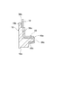
- the third region in the prepared frame body, may be bent so as to have a gap between the second opening side surface of the convex portion and the third region. In this embodiment, when the frame body and the mounting plate are joined, the third region presses the wiring pattern. Therefore, the third region and the wiring pattern can be bonded more firmly.
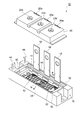
- FIG. 1 is a perspective view of a semiconductor module according to an embodiment.
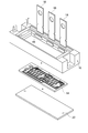
- FIG. 2 is an exploded perspective view of the semiconductor module shown in FIG. 1 and shows a state where a lid is removed from the semiconductor module.
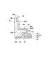
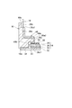
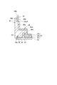
- FIG. 3 is an end view taken along line III-III in FIG.
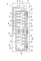
- FIG. 4 is a plan view of a semiconductor chip and a wiring board according to an embodiment.
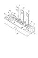
- FIG. 5 is an example of a perspective view of a frame body into which a bus bar is inserted.
- a gate pattern GP2, a source pattern SP2, and a drain pattern DP2 are provided as the wiring pattern 28.
- a MOS-FET 12a is mounted on the drain pattern DP2 so that the back surface drain electrode is electrically connected.
- the gate electrode of the MOS-FET 12a is connected to the gate pattern GP2 via a wire, and the source electrode is connected to the source pattern SP2 via another wire.
- a diode 12b is mounted on the drain pattern DP2.
- the gate pattern GP2 is electrically connected to another gate pattern G2, and the source pattern SP2 is connected to the auxiliary emitter pattern E2 and the source pattern S2 provided at one edge portion of the wiring board 14 through a wire.
- the drain pattern DP2 is connected to a drain pattern D2 provided on one edge of the wiring board 14 via a wire.
- the case 24 accommodates the wiring board 14 on which the semiconductor chip 12 is mounted therein as illustrated in FIG.
- the case 24 may include the frame body 16, the lid body 20, and the heat dissipation plate 22.
- the frame body 16 constitutes the outer peripheral wall of the case 24.
- the frame body 16 surrounds the periphery of the wiring board 14.
- the frame body 16 includes opposing side walls 36 and 38 and connecting portions 40 and 42 that connect the side walls 36 and 38 and the side walls.
- a part of the bus bar 18 is embedded in the side wall 36, and both sides thereof are inserted into the side wall 36 so as to be exposed from the side wall 36.
- an area embedded in the side wall 36 of the bus bar 18 is referred to as a first area 36a
- an area drawn from the side wall 36 on the upper opening (first opening) 16b side of the frame 16 is referred to as a first area 36a.
- the region that is drawn out from the side wall 36 to the inside of the frame 16 is referred to as a second region 36b, and is referred to as a third region 36c.
- the lid 20 can be attached to the frame 16 so as to close the upper opening of the frame 16.
- the lid 20 is formed with a hole 20a and a screw hole 20b.
- the hole 20a is formed in the lid body 20 in order to pull out the second region 36b of the bus bar 18.
- the screw hole 20b is formed in the lid body 20 in order to fix the bus bar 18 drawn out from the hole 20a and bent along the upper surface of the lid body 20 with screws.
- the lid 20 can be manufactured, for example, by molding using a thermosetting resin or a thermoplastic resin.
- the material of the lid 20 is usually the same as the material of the frame 16.
- the frame 16 in which the three bus bars 18 and the four terminals 44 are integrally inserted is prepared.
- the positions of the three bus bars 18 on the side walls 36 and an example of the manufacturing method of the frame 16 with bus bars are as described with reference to FIG.
- the third region 36c may be bent at a shallower angle at the lower corner of the rib 48 (the corner on the lower opening 16a side) than when the entire surface contacts the lower surface 48b.
- the semiconductor module 10 is mounted by attaching the lid 20 to the frame 16. Complete.
Landscapes
- Cooling Or The Like Of Semiconductors Or Solid State Devices (AREA)
- Engineering & Computer Science (AREA)
- Manufacturing & Machinery (AREA)
Abstract
Un module semi-conducteur selon un mode de réalisation de la présente invention est équipé : d'une puce de semi-conducteur ; d'un tableau de connexions ; d'une carte de montage qui est dotée du tableau de connexions monté sur celle-ci ; d'un corps de châssis qui constitue, avec la carte de montage, un boitier permettant de loger le tableau de connexions ; et d'une barre omnibus, qui sort du boitier en étant électriquement connectée au tracé de câblage, et qui est insérée dans une paroi latérale du corps de châssis. Ladite paroi latérale est pourvue d'une partie en saillie qui fait saillie vers l'intérieur du corps de châssis. La barre omnibus est dotée : d'une première région qui est logée dans ladite paroi latérale ; d'une deuxième région qui s'étend vers le côté extérieur du corps de châssis à partir d'une première partie d'extrémité de la première région ; et d'une troisième région qui s'étend vers le côté intérieur du corps de châssis à partir d'une seconde partie d'extrémité de la première région. La troisième région est courbée en fonction de la forme de la partie en saillie du côté du tableau de connexions vue depuis la position de la seconde partie d'extrémité, et la troisième région ainsi que le tracé de câblage sont mis en contact par pression l'un avec l'autre lorsque la carte de montage sur laquelle est monté le tableau de connexions est attachée sur le corps de châssis.
Priority Applications (2)
| Application Number | Priority Date | Filing Date | Title |
|---|---|---|---|
| CN201380028644.5A CN104350594B (zh) | 2012-06-01 | 2013-05-13 | 半导体模块和半导体模块制造方法 |
| EP13796387.2A EP2858109B1 (fr) | 2012-06-01 | 2013-05-13 | Module semi-conducteur et procédé de fabrication d'un module semi-conducteur |
Applications Claiming Priority (2)
| Application Number | Priority Date | Filing Date | Title |
|---|---|---|---|
| JP2012125822A JP5939041B2 (ja) | 2012-06-01 | 2012-06-01 | 半導体モジュール及び半導体モジュールの製造方法 |
| JP2012-125822 | 2012-06-01 |
Publications (1)
| Publication Number | Publication Date |
|---|---|
| WO2013179879A1 true WO2013179879A1 (fr) | 2013-12-05 |
Family
ID=49670004
Family Applications (1)
| Application Number | Title | Priority Date | Filing Date |
|---|---|---|---|
| PCT/JP2013/063290 Ceased WO2013179879A1 (fr) | 2012-06-01 | 2013-05-13 | Module semi-conducteur et procédé de fabrication d'un module semi-conducteur |
Country Status (5)
| Country | Link |
|---|---|
| US (1) | US9263381B2 (fr) |
| EP (1) | EP2858109B1 (fr) |
| JP (1) | JP5939041B2 (fr) |
| CN (1) | CN104350594B (fr) |
| WO (1) | WO2013179879A1 (fr) |
Families Citing this family (13)
| Publication number | Priority date | Publication date | Assignee | Title |
|---|---|---|---|---|
| CN105190882B (zh) * | 2013-03-21 | 2018-04-03 | 三菱电机株式会社 | 半导体装置 |
| JP6299120B2 (ja) * | 2013-09-05 | 2018-03-28 | 富士電機株式会社 | 半導体モジュール |
| JP6323325B2 (ja) * | 2014-04-21 | 2018-05-16 | 三菱電機株式会社 | 半導体装置、半導体装置の製造方法 |
| US10564316B2 (en) | 2014-09-12 | 2020-02-18 | The Climate Corporation | Forecasting national crop yield during the growing season |
| JP6272213B2 (ja) * | 2014-11-26 | 2018-01-31 | 三菱電機株式会社 | 半導体装置 |
| JP6645134B2 (ja) * | 2015-11-16 | 2020-02-12 | 富士電機株式会社 | 半導体装置および半導体装置の製造方法 |
| JP6607077B2 (ja) * | 2016-02-23 | 2019-11-20 | 三菱電機株式会社 | 半導体装置 |
| JP6567996B2 (ja) * | 2016-03-11 | 2019-08-28 | 京セラ株式会社 | パワー半導体モジュール |
| US10028451B2 (en) | 2016-11-16 | 2018-07-24 | The Climate Corporation | Identifying management zones in agricultural fields and generating planting plans for the zones |
| US10398096B2 (en) | 2016-11-16 | 2019-09-03 | The Climate Corporation | Identifying management zones in agricultural fields and generating planting plans for the zones |
| JP6415676B1 (ja) * | 2017-12-07 | 2018-10-31 | 株式会社三社電機製作所 | 半導体モジュール |
| KR102152014B1 (ko) | 2020-03-03 | 2020-09-04 | 제엠제코(주) | 가압형 반도체 패키지 및 이의 제조방법 |
| CN112885241B (zh) * | 2021-02-07 | 2022-12-02 | 业成科技(成都)有限公司 | 框架及其制造方法、显示模组及其测量方法与电子设备 |
Citations (5)
| Publication number | Priority date | Publication date | Assignee | Title |
|---|---|---|---|---|
| JPS63240056A (ja) * | 1986-12-18 | 1988-10-05 | セミクロン エレクトロニク ゲーエムベーハー | 半導体組立ユニット |
| JPH11251514A (ja) | 1998-03-05 | 1999-09-17 | Sansha Electric Mfg Co Ltd | 電力用半導体モジュール |
| JP2001135762A (ja) * | 1999-11-10 | 2001-05-18 | Nissan Motor Co Ltd | 半導体素子の実装構造 |
| JP2006344841A (ja) | 2005-06-10 | 2006-12-21 | Mitsubishi Electric Corp | パワー半導体モジュール |
| WO2009069308A1 (fr) * | 2007-11-30 | 2009-06-04 | Panasonic Corporation | Plaque de base à structure de dissipation de chaleur, module utilisant une plaque de base à structure de dissipation de chaleur, et procédé de fabrication d'une plaque de base à structure de dissipation de chaleur |
Family Cites Families (16)
| Publication number | Priority date | Publication date | Assignee | Title |
|---|---|---|---|---|
| JP3519300B2 (ja) * | 1999-01-11 | 2004-04-12 | 富士電機デバイステクノロジー株式会社 | パワーモジュールのパッケージ構造 |
| DE69937739T2 (de) * | 1999-05-11 | 2008-11-27 | Mitsubishi Denki K.K. | Halbleitervorrichtung |
| JP4218193B2 (ja) * | 2000-08-24 | 2009-02-04 | 三菱電機株式会社 | パワーモジュール |
| JP2003264265A (ja) * | 2002-03-08 | 2003-09-19 | Mitsubishi Electric Corp | 電力用半導体装置 |
| US6933593B2 (en) * | 2003-08-14 | 2005-08-23 | International Rectifier Corporation | Power module having a heat sink |
| JP2006186170A (ja) * | 2004-12-28 | 2006-07-13 | Nissan Motor Co Ltd | 半導体装置 |
| JP4731418B2 (ja) * | 2006-07-10 | 2011-07-27 | 三菱電機株式会社 | 半導体モジュール |
| JP2008252054A (ja) * | 2007-03-06 | 2008-10-16 | Matsushita Electric Ind Co Ltd | 半導体装置および半導体装置の製造方法 |
| JP5166943B2 (ja) * | 2008-04-03 | 2013-03-21 | 矢崎総業株式会社 | バスバーの組付構造 |
| JP5341587B2 (ja) * | 2009-03-23 | 2013-11-13 | 矢崎総業株式会社 | バスバ装置及びヒュージブルリンクユニット |
| JP5611537B2 (ja) * | 2009-04-28 | 2014-10-22 | 日立化成株式会社 | 導電性接合材料、それを用いた接合方法、並びにそれによって接合された半導体装置 |
| JP5617278B2 (ja) * | 2010-02-26 | 2014-11-05 | 株式会社デンソー | 電流検出装置 |
| WO2011149017A1 (fr) * | 2010-05-27 | 2011-12-01 | 京セラ株式会社 | Substrat de module semi-conducteur et module semi-conducteur |
| US8672562B2 (en) * | 2010-08-20 | 2014-03-18 | Sumitomo Electric Industries, Ltd. | Optical transceiver having effective heat conducting path from TOSA to metal housing |
| JP5533431B2 (ja) * | 2010-08-23 | 2014-06-25 | 住友電気工業株式会社 | 光モジュール |
| CN103370788B (zh) * | 2011-04-01 | 2016-10-12 | 富士电机株式会社 | 半导体装置及其制造方法 |
-
2012
- 2012-06-01 JP JP2012125822A patent/JP5939041B2/ja active Active
-
2013
- 2013-05-13 CN CN201380028644.5A patent/CN104350594B/zh active Active
- 2013-05-13 WO PCT/JP2013/063290 patent/WO2013179879A1/fr not_active Ceased
- 2013-05-13 EP EP13796387.2A patent/EP2858109B1/fr active Active
- 2013-05-23 US US13/901,173 patent/US9263381B2/en active Active
Patent Citations (5)
| Publication number | Priority date | Publication date | Assignee | Title |
|---|---|---|---|---|
| JPS63240056A (ja) * | 1986-12-18 | 1988-10-05 | セミクロン エレクトロニク ゲーエムベーハー | 半導体組立ユニット |
| JPH11251514A (ja) | 1998-03-05 | 1999-09-17 | Sansha Electric Mfg Co Ltd | 電力用半導体モジュール |
| JP2001135762A (ja) * | 1999-11-10 | 2001-05-18 | Nissan Motor Co Ltd | 半導体素子の実装構造 |
| JP2006344841A (ja) | 2005-06-10 | 2006-12-21 | Mitsubishi Electric Corp | パワー半導体モジュール |
| WO2009069308A1 (fr) * | 2007-11-30 | 2009-06-04 | Panasonic Corporation | Plaque de base à structure de dissipation de chaleur, module utilisant une plaque de base à structure de dissipation de chaleur, et procédé de fabrication d'une plaque de base à structure de dissipation de chaleur |
Non-Patent Citations (1)
| Title |
|---|
| See also references of EP2858109A4 |
Also Published As
| Publication number | Publication date |
|---|---|
| CN104350594A (zh) | 2015-02-11 |
| US9263381B2 (en) | 2016-02-16 |
| CN104350594B (zh) | 2017-05-10 |
| JP5939041B2 (ja) | 2016-06-22 |
| JP2013251429A (ja) | 2013-12-12 |
| EP2858109A1 (fr) | 2015-04-08 |
| EP2858109B1 (fr) | 2016-08-03 |
| US20130322025A1 (en) | 2013-12-05 |
| EP2858109A4 (fr) | 2015-08-19 |
Similar Documents
| Publication | Publication Date | Title |
|---|---|---|
| JP5939041B2 (ja) | 半導体モジュール及び半導体モジュールの製造方法 | |
| CN106328622B (zh) | 半导体装置及半导体装置的制造方法 | |
| JP6044321B2 (ja) | 半導体モジュール | |
| US7919854B2 (en) | Semiconductor module with two cooling surfaces and method | |
| CN112750801B (zh) | 功率半导体装置 | |
| JP6132034B2 (ja) | 半導体モジュール | |
| JP5935374B2 (ja) | 半導体モジュールの製造方法 | |
| JP2005340639A (ja) | 半導体装置及び三相インバータ装置 | |
| JP2004071977A (ja) | 半導体装置 | |
| CN104600051B (zh) | 半导体模块 | |
| JP4570092B2 (ja) | 半導体モジュール | |
| KR100575216B1 (ko) | 발광소자용 패캐지 베이스 | |
| JP3169578B2 (ja) | 電子部品用基板 | |
| CN114434729B (zh) | 半导体装置用的框体的制造方法 | |
| JP7591377B2 (ja) | 半導体部品 | |
| JP2009158769A (ja) | 半導体装置 | |
| JP2012216654A (ja) | 樹脂成形フレーム及び光半導体装置 | |
| KR20110092779A (ko) | 반도체 파워 모듈 패키지 및 그의 제조방법 | |
| KR20140135443A (ko) | 반도체 모듈의 제조 방법 및 이에 따른 반도체 모듈 | |
| JP2003007379A (ja) | フラット電線の接続構造および接続方法 | |
| US20120146208A1 (en) | Semiconductor module and manufacturing method thereof | |
| CN111916409A (zh) | 一种功率模块及其制作方法 | |
| KR20160051513A (ko) | 전력 모듈 및 그 제조 방법 | |
| KR102551746B1 (ko) | 광원모듈 | |
| JP2012099773A (ja) | 半導体モジュールの製造方法、及び半導体モジュール |
Legal Events
| Date | Code | Title | Description |
|---|---|---|---|
| 121 | Ep: the epo has been informed by wipo that ep was designated in this application |
Ref document number: 13796387 Country of ref document: EP Kind code of ref document: A1 |
|
| REEP | Request for entry into the european phase |
Ref document number: 2013796387 Country of ref document: EP |
|
| WWE | Wipo information: entry into national phase |
Ref document number: 2013796387 Country of ref document: EP |
|
| NENP | Non-entry into the national phase |
Ref country code: DE |