WO2013179914A1 - 反射防止膜、光学系、光学機器、及び反射防止膜の成膜方法 - Google Patents
反射防止膜、光学系、光学機器、及び反射防止膜の成膜方法 Download PDFInfo
- Publication number
- WO2013179914A1 WO2013179914A1 PCT/JP2013/063784 JP2013063784W WO2013179914A1 WO 2013179914 A1 WO2013179914 A1 WO 2013179914A1 JP 2013063784 W JP2013063784 W JP 2013063784W WO 2013179914 A1 WO2013179914 A1 WO 2013179914A1
- Authority
- WO
- WIPO (PCT)
- Prior art keywords
- refractive index
- layer
- antireflection film
- substrate
- low refractive
- Prior art date
- Legal status (The legal status is an assumption and is not a legal conclusion. Google has not performed a legal analysis and makes no representation as to the accuracy of the status listed.)
- Ceased
Links
Images





Classifications
-
- G—PHYSICS
- G02—OPTICS
- G02B—OPTICAL ELEMENTS, SYSTEMS OR APPARATUS
- G02B1/00—Optical elements characterised by the material of which they are made; Optical coatings for optical elements
- G02B1/10—Optical coatings produced by application to, or surface treatment of, optical elements
- G02B1/11—Anti-reflection coatings
-
- G—PHYSICS
- G02—OPTICS
- G02B—OPTICAL ELEMENTS, SYSTEMS OR APPARATUS
- G02B1/00—Optical elements characterised by the material of which they are made; Optical coatings for optical elements
- G02B1/10—Optical coatings produced by application to, or surface treatment of, optical elements
- G02B1/11—Anti-reflection coatings
- G02B1/113—Anti-reflection coatings using inorganic layer materials only
- G02B1/115—Multilayers
-
- G—PHYSICS
- G02—OPTICS
- G02B—OPTICAL ELEMENTS, SYSTEMS OR APPARATUS
- G02B1/00—Optical elements characterised by the material of which they are made; Optical coatings for optical elements
- G02B1/10—Optical coatings produced by application to, or surface treatment of, optical elements
- G02B1/11—Anti-reflection coatings
- G02B1/113—Anti-reflection coatings using inorganic layer materials only
-
- Y—GENERAL TAGGING OF NEW TECHNOLOGICAL DEVELOPMENTS; GENERAL TAGGING OF CROSS-SECTIONAL TECHNOLOGIES SPANNING OVER SEVERAL SECTIONS OF THE IPC; TECHNICAL SUBJECTS COVERED BY FORMER USPC CROSS-REFERENCE ART COLLECTIONS [XRACs] AND DIGESTS
- Y10—TECHNICAL SUBJECTS COVERED BY FORMER USPC
- Y10T—TECHNICAL SUBJECTS COVERED BY FORMER US CLASSIFICATION
- Y10T428/00—Stock material or miscellaneous articles
- Y10T428/24—Structurally defined web or sheet [e.g., overall dimension, etc.]
- Y10T428/24942—Structurally defined web or sheet [e.g., overall dimension, etc.] including components having same physical characteristic in differing degree
Definitions
- the present invention relates to an antireflection film, an optical system having the antireflection film, an optical apparatus having the optical system, and a method for forming the antireflection film.
- the multiphoton absorption microscope uses higher order, for example, second order laser light for the purpose of obtaining high output as excitation light.
- the wavelength of the laser light used for visible light excitation is preferably infrared light.
- the optical system of the multiphoton absorption microscope needs to transmit fluorescence for observation (visible light) and near-infrared light as excitation laser light that generates fluorescence. Therefore, an antireflection film that transmits near-infrared light from visible light has been required.
- the laser light as the excitation light needs to have a wavelength approximately twice the fluorescence observation wavelength. In fluorescence observation, the wavelength used for observation is determined by the reagent used. Since the wavelength of visible light used is about 500 nm, it is preferable that the antireflection film transmits light having a wavelength from visible light to near infrared (about 1000 nm).
- Patent Document 1 proposes an antireflection film that transmits only near-infrared light that does not include visible light. Furthermore, since it is required to block near-infrared light when visible light is necessary, as in Patent Document 2, visible light is transmitted and near-infrared light is reflected. Antireflection films have been proposed. Further, as an antireflection film that transmits visible light to near-infrared light, Patent Document 3 discloses an antireflection film that transmits light in the wavelength range of 400 nm to 1100 nm.
- the multiphoton absorption microscope not only the surface of the observation target but also the inside can be observed.
- a laser beam having a longer wavelength as excitation light in order to observe the deep portion.
- the antireflection film described in Patent Document 1 can transmit only one of visible light and near-infrared light.
- the antireflection film described in Patent Document 3 has insufficient transmission band width, has a reflectance of 7% at a wavelength of 1350 nm, and a reflectance of 16% at a wavelength of 1600 nm. Therefore, it does not serve as an antireflection film.
- the present invention has been made in view of the above, and an object thereof is to provide an antireflection film having a band from visible light to infrared region (wavelength range: 400 nm to 1600 nm).
- the antireflection film according to the present invention alternately stacks a high refractive index material and a low refractive index material having a refractive index lower than that of the high refractive index material, An ultra-low refractive index material having a refractive index lower than that of the low refractive index material is laminated on the outermost layer to form 12 layers.
- the optical system according to the present invention is characterized by being composed of one or more optical substrates having the above-described antireflection film.
- the optical apparatus according to the present invention is characterized by having the above-described optical system.
- a method for forming an antireflection film according to the present invention includes: a first film forming step of alternately stacking a high refractive index material and a low refractive index material having a lower refractive index than the high refractive index material on a substrate; And a second film forming step of laminating an ultra-low refractive index material having a refractive index lower than that of the low refractive index material on the outermost layer by wet coating.
- the antireflection film according to the present invention can provide an antireflection film having a band from visible light to infrared region (wavelength range: 400 nm to 1600 nm). Further, an antireflection film having a reflectance of 1% or less in the wavelength range of 400 nm to 1600 nm can be realized by forming a wet coat layer on the outermost layer and laminating a dielectric multilayer film on the other layers. By forming this antireflection film on the optical component, a longer wavelength laser beam can be used as the excitation light, and deeper observation can be performed in the internal observation of the observation target.
- 6 is a table showing a layer configuration of an antireflection film according to Example 1, Example 2, Example 3, and Example 4.
- 10 is a table showing the maximum reflectance of the antireflection film according to Example 1, Example 2, Example 3, and Example 4.
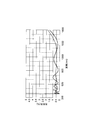
- 6 is a graph showing the reflectance characteristics of the antireflection film according to Example 1.
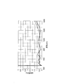
- 6 is a graph showing the reflectance characteristics of an antireflection film according to Example 2.
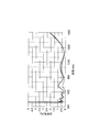
- 6 is a graph showing the reflectance characteristics of an antireflection film according to Example 3.
- 6 is a graph showing the reflectance characteristics of an antireflection film according to Example 4.
- 10 is a table showing a layer configuration of an antireflection film according to Example 5 and Example 6.
- FIG. 10 is a graph showing the reflectance characteristics of an antireflection film according to Example 5.
- 10 is a graph showing the reflectance characteristics of an antireflection film according to Example 6.
- 10 is a table showing a layer configuration of an antireflection film according to Example 7 and Example 8.
- 10 is a table showing the maximum reflectance of an antireflection film according to Example 7 and Example 8.
- 12 is a graph showing the reflectance characteristics of an antireflection film according to Example 7.
- 10 is a graph showing the reflectance characteristics of an antireflection film according to Example 8.
- FIG. 1 is a diagram showing a schematic configuration of a multiphoton absorption microscope according to an embodiment of the optical apparatus of the present invention.
- the short pulse laser light oscillated by the laser light source 101 is reflected by the multilayer filter 102 and irradiated to the observation object S placed on the observation table 103 via the optical system 110.
- the excitation light generated in the observation object S by the laser light irradiation passes through the multilayer filter 102 and can be observed by the observer B.
- the optical system 110 is formed with an antireflection film, and has a reflectance of 1% or less with respect to light having a wavelength range of 400 nm to 1600 nm.
- This antireflection film consists of 12 layers laminated in order on the substrate, and the twelfth layer (the outermost layer) farthest from the substrate is mainly composed of hollow silica, which is an ultra-low refractive index material, and is formed by wet coating. It is an ultra-low refractive index layer.
- a wet coating forming method for example, spin coating, dipping, spraying, ink jetting, and slit water can be used. Further, the refractive index of the ultra-low refractive index layer by wet coating can be set to an arbitrary value between 1.20 and 1.29.
- the first to eleventh layers are formed by sequentially laminating dielectric multilayer films.
- the first to eleventh layers are formed by, for example, vacuum deposition, IAD (Ion Assisted Deposition), assistance by plasma, sputtering, or ion beam sputtering (first film formation step).
- IAD Ion Assisted Deposition
- first film formation step After this film formation, an ultra-low refractive index substance is laminated on the 11th layer as the outermost layer (second film formation step).
- the optical system in the multiphoton absorption microscope of the present embodiment is preferably used for an objective lens for a multiphoton absorption microscope, but it is also applicable to lenses, prisms, and filters of optical devices such as cameras, glasses, and telescopes. Can do.
- the anti-reflective film of the embodiment of the present invention is an ultra-low refractive index in which a high refractive index material and a low refractive index material having a lower refractive index than that of the high refractive index material are alternately stacked, and the refractive index is lower than that of the low refractive index material It is characterized in that the rate material is laminated on the outermost layer to form 12 layers.
- the first, third, fifth, seventh, ninth, and eleventh layers are made of a high refractive index material, and the second, fourth, sixth, eighth, and tenth layers are made low refractive.
- the refractive index material is preferably laminated on the twelfth layer.
- the optical film thickness of the eleventh layer (11th layer) from the substrate is preferably 4% or less of the entire optical film thickness of the antireflection film.
- the optical film thickness nd represented by the product of the refractive index n and the physical film thickness d in each layer preferably satisfies the following expressions.
- the optical film thickness nd in each layer does not satisfy the above formulas, it becomes difficult to realize a reflectance of 1% or less for light in the wavelength range of 400 nm to 1600 nm.
- the high refractive index material is TiO 2 , Ta 2 O 5 , HfO 2 , Nb 2 O 5 , or a mixture thereof with La and Zr, and the low refractive index material is SiO 2.
- MgF 2 or a mixture thereof is preferable.
- the refractive index of the ultra-low refractive index material is preferably 1.20 to 1.29.
- the refractive index is lower than 1.20, it is difficult to select an applicable substance.
- the refractive index is higher than 1.29, it is difficult to realize a reflectance of 1% or less with respect to light having a wavelength range of 400 nm to 1600 nm.
- the refractive index of the substrate is preferably in the range of 1.44 to 1.88.
- the refractive index of the substrate is outside the range of 1.44 to 1.88, it becomes difficult to realize a reflectance of 1% or less for light in the wavelength range of 400 nm to 1600 nm.
- the ultra low refractive index material is formed by wet coating.
- An optical system according to an embodiment of the present invention is characterized in that it is composed of one or more optical substrates having any of the above-described antireflection films.
- An optical apparatus has the above-described optical system.
- the method of forming an antireflection film according to an embodiment of the present invention includes a first film forming step of alternately stacking a high refractive index material and a low refractive index material having a lower refractive index than the high refractive index material on a substrate. And a second film forming step of laminating an ultra-low refractive index material having a refractive index lower than that of the low refractive index material on the outermost layer by wet coating.
- the first film formation process is performed by vacuum deposition, IAD, assistance by plasma, sputtering, or ion beam sputtering.
- FIG. 2 is a table showing the layer configuration of the antireflection film according to Example 1, Example 2, Example 3, and Example 4.
- FIG. 3 is a table showing the maximum reflectance of the antireflection films according to Example 1, Example 2, Example 3, and Example 4.
- FIG. 4 is a graph showing the reflectance characteristics of the antireflection film according to Example 1.
- FIG. 5 is a graph showing the reflectance characteristics of the antireflection film according to Example 2.
- FIG. 6 is a graph showing the reflectance characteristics of the antireflection film according to Example 3.
- FIG. 7 is a graph showing the reflectance characteristics of the antireflection film according to Example 4.
- FIG. 2 shows the optical film thickness of each layer at the design wavelength of 550 nm.
- FIG. 3 shows the maximum reflectivity when the refractive index of the substrate is the minimum value and the maximum value in the substrate refractive index range shown in FIG. These maximum reflectivities are the maximum reflectivities in the wavelength range of 400 nm to 1600 nm.
- the case where the refractive index n of the substrate is 1.44 is indicated by a solid line, and the case where it is 1.55 is indicated by a broken line.
- FIG. 4 shows the case where the refractive index n of the substrate is 1.44 a solid line, and the case where it is 1.55 is indicated by a broken line.
- the case where the refractive index n of the substrate is 1.55 is indicated by a solid line, and the case where it is 1.70 is indicated by a broken line.
- the case where the refractive index n of the substrate is 1.70 is indicated by a solid line, and the case where it is 1.81 is indicated by a broken line.
- the case where the refractive index n of the substrate is 1.81 is indicated by a solid line, and the case where it is 1.88 is indicated by a broken line.
- Ta 2 O 5 as a high refractive index material is arranged as a high refractive index layer of the first, third, fifth, seventh, ninth, and eleventh layers in order from the substrate side.
- SiO 2 is arranged as the low refractive index layers of the second, fourth, sixth, eighth, and tenth layers in order from the substrate side, and the ultra low refractive index substance is the twelfth layer (the outermost layer, the ultra low layer). (Refractive index layer).
- the optical film thickness that is the product of the refractive index n and the physical film thickness d satisfies the following expressions.
- 8th layer 0.05 ⁇ nd ⁇ 0.17 Ninth layer 0.06 ⁇ nd ⁇ 0.15 10th layer 0.16 ⁇ nd ⁇ 0.27 11th layer 0.02 ⁇ nd ⁇ 0.06 12th layer 0.32 ⁇ nd ⁇ 0.39
- Example 1 As shown in FIG. 4, the antireflection film of Example 1 has a reflectance of 1% or less in a wavelength range of 400 nm to 1600 nm on both substrates having a refractive index of 1.44 and a refractive index of 1.55. Yes. The same applies to a substrate having a refractive index in the range between a refractive index of 1.44 and a refractive index of 1.55.
- the maximum reflectance is 0.92%, and the maximum reflectance does not exceed 1%.
- Example 2 As shown in FIG. 5, the antireflection film of Example 2 has a reflectance of 1% or less in a wavelength range of 400 nm to 1600 nm on any substrate having a refractive index of 1.55 and a refractive index of 1.70. Yes. The same applies to a substrate having a refractive index in the range between a refractive index of 1.55 and a refractive index of 1.70.
- the maximum reflectance is 0.97%, and the maximum reflectance does not exceed 1%.
- Example 3 As shown in FIG. 6, the antireflection film of Example 3 has a reflectance of 1% or less in a wavelength range of 400 nm to 1600 nm on both substrates having a refractive index of 1.70 and a refractive index of 1.81. Yes. The same applies to a substrate having a refractive index in the range between a refractive index of 1.70 and a refractive index of 1.81.
- the maximum reflectance is 0.93%, and the maximum reflectance does not exceed 1%.
- Example 4 As shown in FIG. 7, the antireflection film of Example 4 has a reflectance of 1% or less in a wavelength range of 400 nm to 1600 nm on both substrates having a refractive index of 1.81 and a refractive index of 1.88. Yes. The same applies to a substrate having a refractive index in the range between a refractive index of 1.81 and a refractive index of 1.88.
- the maximum reflectance is 0.95%, and the maximum reflectance does not exceed 1%.
- FIG. 8 is a table showing the layer configuration of the antireflection film according to Example 5 and Example 6.
- FIG. 9 is a table showing the maximum reflectance of the antireflection film according to Example 5 and Example 6.
- FIG. 10 is a graph showing the reflectance characteristics of the antireflection film according to Example 5.
- FIG. 11 is a graph showing the reflectance characteristics of the antireflection film according to Example 6.
- FIG. 8 shows the optical film thickness of each layer at the design wavelength of 550 nm.
- FIG. 9 shows the maximum reflectivity when the refractive index of the substrate is the minimum value and the maximum value in the substrate refractive index range shown in FIG. These maximum reflectivities are the maximum reflectivities in the wavelength range of 400 nm to 1600 nm.
- the case where the refractive index n of the substrate is 1.70 is indicated by a solid line
- the case where it is 1.45 is indicated by a broken line
- the case where it is 1.88 is indicated by a one-dot chain line.
- FIG. 11 the case where the refractive index n of the substrate is 1.44 is indicated by a solid line, and the case where it is 1.88 is indicated by a broken line.
- HfO 2 as a high refractive index material is arranged as a high refractive index layer of first, third, fifth, seventh, ninth and eleventh layers in order from the substrate side, and SiO as a low refractive index material.
- the ultra low refractive index substance is the twelfth layer (the outermost layer, the ultra low refractive index). Layer).
- the optical film thickness that is the product of the refractive index n and the physical film thickness d satisfies the following expressions.
- 8th layer 0.05 ⁇ nd ⁇ 0.17 Ninth layer 0.06 ⁇ nd ⁇ 0.15 10th layer 0.16 ⁇ nd ⁇ 0.27 11th layer 0.02 ⁇ nd ⁇ 0.06 12th layer 0.32 ⁇ nd ⁇ 0.39
- Example 5 As shown in FIG. 10, the antireflection film of Example 5 has a reflectance of 1% or less in a wavelength range of 400 nm to 1600 nm on any substrate having a refractive index of 1.44, 1.70, and 1.88. It has become. The same applies to a substrate having a refractive index in the range between the refractive indexes of 1.44, 1.70, and 1.88.
- Example 6 As shown in FIG. 11, the antireflection film of Example 6 has a reflectance of 1% or less in a wavelength range of 400 nm to 1600 nm on both substrates having a refractive index of 1.44 and a refractive index of 1.88. Yes. The same applies to a substrate having a refractive index in the range between a refractive index of 1.44 and a refractive index of 1.88.
- the maximum reflectance is 0.95%, and the maximum reflectance does not exceed 1%.
- FIG. 12 is a table showing the layer configuration of the antireflection film according to Example 7 and Example 8.
- FIG. 13 is a table showing the maximum reflectance of the antireflection film according to Example 7 and Example 8.
- FIG. 14 is a graph showing the reflectance characteristics of the antireflection film according to Example 7.
- FIG. 15 is a graph showing the reflectance characteristics of the antireflection film according to Example 8.
- FIG. 12 shows the optical film thickness of each layer at the design wavelength of 550 nm.
- FIG. 13 shows the maximum reflectivity when the refractive index of the substrate is the minimum value and the maximum value in the substrate refractive index range shown in FIG. These maximum reflectivities are the maximum reflectivities in the wavelength range of 400 nm to 1600 nm.
- FIG. 14 the case where the refractive index n of the substrate is 1.44 is indicated by a solid line, and the case where it is 1.88 is indicated by a broken line.
- FIG. 15 the case where the refractive index n of the substrate is 1.44 is indicated by a solid line, and the case where it is 1.88 is indicated by a broken line.
- TiO 2 as a high refractive index material is disposed as a high refractive index layer of first, third, fifth, seventh, ninth, and eleventh layers in order from the substrate side, and MgF as a low refractive index material.
- the ultra low refractive index substance is the twelfth layer (the outermost layer, the ultra low refractive index). Layer).
- the optical film thickness that is the product of the refractive index n and the physical film thickness d satisfies the following expressions.
- 8th layer 0.05 ⁇ nd ⁇ 0.17 Ninth layer 0.06 ⁇ nd ⁇ 0.15 10th layer 0.16 ⁇ nd ⁇ 0.27 11th layer 0.02 ⁇ nd ⁇ 0.06 12th layer 0.32 ⁇ nd ⁇ 0.39
- Example 7 As shown in FIG. 14, the antireflection film of Example 7 has a reflectance of 1% or less in a wavelength range of 400 nm to 1600 nm on both substrates having a refractive index of 1.44 and a refractive index of 1.88. Yes. The same applies to a substrate having a refractive index in the range between a refractive index of 1.44 and a refractive index of 1.88.
- the maximum reflectance is 0.80%, and the maximum reflectance does not exceed 1%.
- Example 8 As shown in FIG. 15, the antireflection film of Example 8 has a reflectance of 1% or less in a wavelength range of 400 nm to 1600 nm on both substrates having a refractive index of 1.44 and a refractive index of 1.88. Yes. The same applies to a substrate having a refractive index in the range between a refractive index of 1.44 and a refractive index of 1.88.
- the maximum reflectance is 0.92%, and the maximum reflectance does not exceed 1%.
- the antireflection film according to the present invention is useful for a multiphoton absorption microscope in which an objective lens needs an antireflection film having a wavelength range from visible light to infrared.
Landscapes
- Physics & Mathematics (AREA)
- General Physics & Mathematics (AREA)
- Optics & Photonics (AREA)
- Chemical & Material Sciences (AREA)
- Inorganic Chemistry (AREA)
- Surface Treatment Of Optical Elements (AREA)
- Laminated Bodies (AREA)
Description
本発明は、反射防止膜、この反射防止膜を有する光学系、この光学系を有する光学機器、及び反射防止膜の成膜方法に関するものである。
近年、医療、化学分野において、細胞等の観察対象に蛍光たんぱく質を含む試薬を投与し、ある一定の波長の光をあてると、試薬から別の波長の蛍光が励起され、この蛍光によって対象の観察を行うことができる蛍光顕微鏡の用途が拡大している。そのような蛍光顕微鏡の一つとして、多光子吸収顕微鏡がある。
多光子吸収顕微鏡は、励起光として高出力を得る目的から、高次、例えば2次のレーザ光を用いる。ここでは、可視光励起のために用いるレーザ光の波長は、赤外光が好ましい。
この場合、多光子吸収顕微鏡の光学系は、観察用の蛍光(可視光)と、蛍光を発生させる励起レーザ光としての近赤外光と、を透過させる必要がある。そのため、可視光から近赤外光を透過させる反射防止膜が必要とされてきた。ここで、励起光としてのレーザ光は、蛍光観察波長の約2倍の波長が必要になる。蛍光観察では、使用される試薬によって観察に使われる波長が決定する。使用される可視光の波長はおおよそ500nm前後であるので、反射防止膜は、可視光から近赤外(約1000nm)までの波長の光を透過することが好ましい。
この場合、多光子吸収顕微鏡の光学系は、観察用の蛍光(可視光)と、蛍光を発生させる励起レーザ光としての近赤外光と、を透過させる必要がある。そのため、可視光から近赤外光を透過させる反射防止膜が必要とされてきた。ここで、励起光としてのレーザ光は、蛍光観察波長の約2倍の波長が必要になる。蛍光観察では、使用される試薬によって観察に使われる波長が決定する。使用される可視光の波長はおおよそ500nm前後であるので、反射防止膜は、可視光から近赤外(約1000nm)までの波長の光を透過することが好ましい。
一般的な反射防止膜として、可視光(波長範囲400nm~680nm)を透過させるものであって、3層構成の設計が知られている。また、特許文献1では可視光を含まない近赤外域光のみを透過させる反射防止膜が提案されている。さらにまた、可視光が必要な場合には近赤外域の光を遮断することが求められるため、特許文献2のように、可視光は透過させ、近赤外域の光は反射させる、という特性の反射防止膜が提案されている。また、可視光から近赤外域光を透過させる反射防止膜としては、特許文献3において波長範囲400nm~1100nmまで透過させる反射防止膜が得られている。
多光子吸収顕微鏡においては、観察対象の表面だけでなく、内部の観察を行うことができる。多光子吸収顕微鏡を用いて観察対象の内部観察を行うとき、その深部を観察するには、より長波長のレーザ光を励起光に使用することが有効となる。また、大気の光吸収などを考慮すると、波長1600nmまでの長波長のレーザ光を使用できると良い。つまり、波長範囲400nm~1600nmという範囲の透過帯域があることが望ましい。したがって、従来の多光子吸収顕微鏡においては、観察を行うための対物レンズに波長範囲400nm~1600nmの反射防止膜が必要となる。
しかし、上述のように、特許文献1に記載されている反射防止膜では、可視光か近赤外域かのどちらか一方の光しか透過させることができない。また、特許文献3に記載されている反射防止膜では透過帯域の幅が足りず、波長1350nmで反射率7%、波長1600nmでは反射率16%となっており、レンズや基板以上の反射率となっているため、反射防止膜の役目を果たしていない。
本発明は、上記に鑑みてなされたものであって、可視光から赤外域(波長範囲400nm~1600nm)までの帯域を持つ反射防止膜を提供することを目的とする。
上述した課題を解決し、目的を達成するために、本発明に係る反射防止膜は、高屈折率物質と、高屈折率物質より屈折率が低い低屈折率物質と、を交互に積層し、低屈折率物質より屈折率が低い超低屈折率物質を最表層に積層して12層としたことを特徴としている。
本発明に係る光学系は、上述の反射防止膜を有する1枚以上の光学基板で構成されたことを特徴としている。
本発明に係る光学機器は、上述の光学系を有することを特徴としている。
本発明に係る反射防止膜の成膜方法は、基板上に、高屈折率物質と、高屈折率物質より屈折率が低い低屈折率物質と、を交互に積層する第1成膜工程と、低屈折率物質より屈折率が低い超低屈折率物質を、ウエットコートによって最表層に積層する第2成膜工程と、を備えることを特徴としている。
本発明に係る反射防止膜は、可視光から赤外域(波長範囲400nm~1600nm)までの帯域を持つ反射防止膜を提供することができる。
また、最表層にウエットコートによる層を形成し、他の層に誘電体多層膜を積層した構成により、波長範囲400nm~1600nmで1%以下の反射率の反射防止膜を実現することができる。この反射防止膜を光学部品に成膜することで、励起光として、より長波長のレーザ光を使用することができ、観察対象の内部観察において、より深部の観察を行うことができる。
また、最表層にウエットコートによる層を形成し、他の層に誘電体多層膜を積層した構成により、波長範囲400nm~1600nmで1%以下の反射率の反射防止膜を実現することができる。この反射防止膜を光学部品に成膜することで、励起光として、より長波長のレーザ光を使用することができ、観察対象の内部観察において、より深部の観察を行うことができる。
以下に、本発明に係る反射防止膜、この反射防止膜を有する光学系、この光学系を有する光学機器、及び反射防止膜の成膜方法の実施形態を図面に基づいて詳細に説明する。なお、以下の実施形態によりこの発明が限定されるものではない。
図1は、本発明の光学機器の実施形態に係る多光子吸収顕微鏡の概略構成を示す図である。
図1に示す多光子吸収顕微鏡においては、レーザ光源101で発振させた短パルスレーザ光を多層膜フィルタ102で反射させ、光学系110を介して、観察台103上に置いた観察対象Sに照射する。このレーザ光の照射によって観察対象Sで発生した励起光は、多層膜フィルタ102を透過して観察者Bによる観察が可能となる。
図1に示す多光子吸収顕微鏡においては、レーザ光源101で発振させた短パルスレーザ光を多層膜フィルタ102で反射させ、光学系110を介して、観察台103上に置いた観察対象Sに照射する。このレーザ光の照射によって観察対象Sで発生した励起光は、多層膜フィルタ102を透過して観察者Bによる観察が可能となる。
光学系110には、反射防止膜が形成されており、波長範囲400nm~1600nmの光に対して1%以下の反射率を有している。
この反射防止膜は、基板上に順に積層された12層からなり、基板から最も離れた第12層(最表層)は、超低屈折率物質である中空シリカを主成分とし、ウエットコートによって形成される超低屈折率層である。ウエットコートの形成方法としては、例えば、スピンコート、ディッピング、スプレー、インクジェット、スリットウォーターが使用可能である。また、ウエットコートによる超低屈折率層の屈折率は1.20~1.29の間で任意の値に設定できる。
この反射防止膜は、基板上に順に積層された12層からなり、基板から最も離れた第12層(最表層)は、超低屈折率物質である中空シリカを主成分とし、ウエットコートによって形成される超低屈折率層である。ウエットコートの形成方法としては、例えば、スピンコート、ディッピング、スプレー、インクジェット、スリットウォーターが使用可能である。また、ウエットコートによる超低屈折率層の屈折率は1.20~1.29の間で任意の値に設定できる。
第1層~第11層は、誘電体多層膜を順に積層してなる。この第1層~第11層は、例えば、真空蒸着、IAD(Ion Assisted Deposition)、プラズマによるアシスト、スパッタリング、イオンビームスパッタによって成膜する(第1成膜工程)。この成膜の後に、最表層として、第11層上に超低屈折率物質を積層する(第2成膜工程)。
本実施形態の多光子吸収顕微鏡における光学系は、多光子吸収顕微鏡用の対物レンズに用いることが望ましいが、カメラ、眼鏡、望遠鏡等の光学機器のレンズ、プリズム、フィルタに対しても適用することができる。
次に、本発明の実施形態に係る反射防止膜の構成・作用・効果について説明する。
本発明の実施形態の反射防止膜は、高屈折率物質と、高屈折率物質より屈折率が低い低屈折率物質と、を交互に積層し、低屈折率物質より屈折率が低い超低屈折率物質を最表層に積層して12層としたことを特徴としている。
本発明の実施形態の反射防止膜において、基板側から順に、第1、3、5、7、9、11層に高屈折率物質を、第2、4、6、8、10層に低屈折率物質を、第12層に超低屈折率物質を積層することが好ましい。
本発明の実施形態の反射防止膜において、基板から11番目の層(第11層)の光学膜厚は、反射防止膜の全体の光学膜厚の4%以下であることが好ましい。
本発明の実施形態の反射防止膜においては、各層において、屈折率nと物理膜厚dの積で表される光学膜厚ndが、次の各式を満足することが好ましい。
第1層 0.02<nd<0.11
第2層 0.03<nd<0.22
第3層 0.06<nd<0.26
第4層 0.03<nd<0.18
第5層 0.09<nd<0.32
第6層 0.02<nd<0.16
第7層 0.10<nd<0.73
第8層 0.05<nd<0.17
第9層 0.06<nd<0.15
第10層 0.16<nd<0.27
第11層 0.02<nd<0.06
第12層 0.32<nd<0.39
各層における光学膜厚ndが、上記各式を満足しない場合は、波長範囲400nm~1600nmの光に対して1%以下の反射率を実現することが難しくなる。
第1層 0.02<nd<0.11
第2層 0.03<nd<0.22
第3層 0.06<nd<0.26
第4層 0.03<nd<0.18
第5層 0.09<nd<0.32
第6層 0.02<nd<0.16
第7層 0.10<nd<0.73
第8層 0.05<nd<0.17
第9層 0.06<nd<0.15
第10層 0.16<nd<0.27
第11層 0.02<nd<0.06
第12層 0.32<nd<0.39
各層における光学膜厚ndが、上記各式を満足しない場合は、波長範囲400nm~1600nmの光に対して1%以下の反射率を実現することが難しくなる。
本発明の実施形態の反射防止膜において、高屈折率物質はTiO2、Ta2O5、HfO2、Nb2O5、又はそれらとLa、Zrの混合物であり、低屈折率物質はSiO2、MgF2、又はそれらの混合物であることが好ましい。
本発明の実施形態の反射防止膜において、超低屈折率物質の屈折率は1.20~1.29であることが好ましい。
屈折率が1.20を下回ると適用可能な物質の選択が困難となり、1.29を上回ると、波長範囲400nm~1600nmの光に対して1%以下の反射率を実現することが難しくなる。
屈折率が1.20を下回ると適用可能な物質の選択が困難となり、1.29を上回ると、波長範囲400nm~1600nmの光に対して1%以下の反射率を実現することが難しくなる。
本発明の実施形態の反射防止膜において、基板の屈折率は1.44~1.88の範囲であることが好ましい。
基板の屈折率が1.44~1.88の範囲外となると、波長範囲400nm~1600nmの光に対して1%以下の反射率を実現することが難しくなる。
基板の屈折率が1.44~1.88の範囲外となると、波長範囲400nm~1600nmの光に対して1%以下の反射率を実現することが難しくなる。
本発明の実施形態の反射防止膜において、超低屈折率物質は、ウエットコートによって膜を形成することが好ましい。
本発明の実施形態の光学系は、上述のいずれかの反射防止膜を有する1枚以上の光学基板で構成されたことを特徴としている。
本発明の実施形態の光学機器は、上述の光学系を有することを特徴としている。
本発明の実施形態の反射防止膜の成膜方法は、基板上に、高屈折率物質と、高屈折率物質より屈折率が低い低屈折率物質と、を交互に積層する第1成膜工程と、低屈折率物質より屈折率が低い超低屈折率物質を、ウエットコートによって最表層に積層する第2成膜工程と、を備えることを特徴としている。
本発明の実施形態の反射防止膜の成膜方法において、第1成膜工程においては、真空蒸着、IAD、プラズマによるアシスト、スパッタリング、又はイオンビームスパッタによって成膜することが好ましい。
つづいて、本発明の実施形態に係る反射防止膜の実施例について説明する。
(実施例1~4)
図2は、実施例1、実施例2、実施例3、及び実施例4に係る反射防止膜の層構成を示す表である。図3は、実施例1、実施例2、実施例3、及び実施例4に係る反射防止膜の最大反射率を示す表である。図4は、実施例1に係る反射防止膜の反射率特性を示すグラフである。図5は、実施例2に係る反射防止膜の反射率特性を示すグラフである。図6は、実施例3に係る反射防止膜の反射率特性を示すグラフである。図7は、実施例4に係る反射防止膜の反射率特性を示すグラフである。
(実施例1~4)
図2は、実施例1、実施例2、実施例3、及び実施例4に係る反射防止膜の層構成を示す表である。図3は、実施例1、実施例2、実施例3、及び実施例4に係る反射防止膜の最大反射率を示す表である。図4は、実施例1に係る反射防止膜の反射率特性を示すグラフである。図5は、実施例2に係る反射防止膜の反射率特性を示すグラフである。図6は、実施例3に係る反射防止膜の反射率特性を示すグラフである。図7は、実施例4に係る反射防止膜の反射率特性を示すグラフである。
図2においては、設計波長550nmにおける各層の光学膜厚を示している。光学膜厚は、各層の屈折率nと物理膜厚dの積であって、設計波長/4=0.25で表している。
図3は、基板の屈折率が、図3に示す基板屈折率範囲の最小値である場合と最大値である場合のそれぞれについて、最大反射率を示している。これらの最大反射率は、波長範囲400nm~1600nmにおける最大反射率である。
図4においては、基板の屈折率nが1.44である場合を実線で示し、1.55である場合を破線で示している。
図5においては、基板の屈折率nが1.55である場合を実線で示し、1.70である場合を破線で示している。
図6においては、基板の屈折率nが1.70である場合を実線で示し、1.81である場合を破線で示している。
図7においては、基板の屈折率nが1.81である場合を実線で示し、1.88である場合を破線で示している。
図3は、基板の屈折率が、図3に示す基板屈折率範囲の最小値である場合と最大値である場合のそれぞれについて、最大反射率を示している。これらの最大反射率は、波長範囲400nm~1600nmにおける最大反射率である。
図4においては、基板の屈折率nが1.44である場合を実線で示し、1.55である場合を破線で示している。
図5においては、基板の屈折率nが1.55である場合を実線で示し、1.70である場合を破線で示している。
図6においては、基板の屈折率nが1.70である場合を実線で示し、1.81である場合を破線で示している。
図7においては、基板の屈折率nが1.81である場合を実線で示し、1.88である場合を破線で示している。
実施例1~4の反射防止膜は、図2に示すように、基板上に、高屈折率物質としてのTa2O5(屈折率n=2.22)と、低屈折率物質としてのSiO2(屈折率n=1.45)と、を交互に積層させて11層とし、さらに基板から遠い側に超低屈折率物質を積層させた、12層の積層体である。
高屈折率物質としてのTa2O5は、基板側から順に、第1、第3、第5、第7、第9、及び第11層の高屈折率層として配置され、低屈折率物質としてのSiO2は、基板側から順に、第2、第4、第6、第8、及び第10層の低屈折率層として配置され、超低屈折率物質は第12層(最表層、超低屈折率層)として配置されている。
高屈折率物質としてのTa2O5は、基板側から順に、第1、第3、第5、第7、第9、及び第11層の高屈折率層として配置され、低屈折率物質としてのSiO2は、基板側から順に、第2、第4、第6、第8、及び第10層の低屈折率層として配置され、超低屈折率物質は第12層(最表層、超低屈折率層)として配置されている。
ここで、積層体の各層において、屈折率nと物理膜厚dの積である光学膜厚が、次の各式を満足している。
第1層 0.02<nd<0.11
第2層 0.03<nd<0.22
第3層 0.06<nd<0.26
第4層 0.03<nd<0.18
第5層 0.09<nd<0.32
第6層 0.02<nd<0.16
第7層 0.10<nd<0.73
第8層 0.05<nd<0.17
第9層 0.06<nd<0.15
第10層 0.16<nd<0.27
第11層 0.02<nd<0.06
第12層 0.32<nd<0.39
第1層 0.02<nd<0.11
第2層 0.03<nd<0.22
第3層 0.06<nd<0.26
第4層 0.03<nd<0.18
第5層 0.09<nd<0.32
第6層 0.02<nd<0.16
第7層 0.10<nd<0.73
第8層 0.05<nd<0.17
第9層 0.06<nd<0.15
第10層 0.16<nd<0.27
第11層 0.02<nd<0.06
第12層 0.32<nd<0.39
(実施例1)
図4に示すように、実施例1の反射防止膜は、屈折率1.44及び屈折率1.55のいずれの基板上においても、波長範囲400nm~1600nmで反射率が1%以下となっている。屈折率1.44と屈折率1.55の間の範囲の屈折率の基板においても同様である。
図4に示すように、実施例1の反射防止膜は、屈折率1.44及び屈折率1.55のいずれの基板上においても、波長範囲400nm~1600nmで反射率が1%以下となっている。屈折率1.44と屈折率1.55の間の範囲の屈折率の基板においても同様である。
具体的には、図3に示すように、屈折率が最小(n=1.44)の基板に形成した反射防止膜では、最大反射率は0.84%であり、屈折率が最大(n=1.55)の基板に形成した反射防止膜では、最大反射率は0.92%であって、最大反射率は1%を超えていない。
(実施例2)
図5に示すように、実施例2の反射防止膜は、屈折率1.55及び屈折率1.70のいずれの基板上においても、波長範囲400nm~1600nmで反射率が1%以下となっている。屈折率1.55と屈折率1.70の間の範囲の屈折率の基板においても同様である。
図5に示すように、実施例2の反射防止膜は、屈折率1.55及び屈折率1.70のいずれの基板上においても、波長範囲400nm~1600nmで反射率が1%以下となっている。屈折率1.55と屈折率1.70の間の範囲の屈折率の基板においても同様である。
具体的には、図3に示すように、屈折率が最小(n=1.55)の基板に形成した反射防止膜では、最大反射率は0.97%であり、屈折率が最大(n=1.70)の基板に形成した反射防止膜では、最大反射率は0.97%であって、最大反射率は1%を超えていない。
(実施例3)
図6に示すように、実施例3の反射防止膜は、屈折率1.70及び屈折率1.81のいずれの基板上においても、波長範囲400nm~1600nmで反射率が1%以下となっている。屈折率1.70と屈折率1.81の間の範囲の屈折率の基板においても同様である。
図6に示すように、実施例3の反射防止膜は、屈折率1.70及び屈折率1.81のいずれの基板上においても、波長範囲400nm~1600nmで反射率が1%以下となっている。屈折率1.70と屈折率1.81の間の範囲の屈折率の基板においても同様である。
具体的には、図3に示すように、屈折率が最小(n=1.70)の基板に形成した反射防止膜では、最大反射率は0.98%であり、屈折率が最大(n=1.81)の基板に形成した反射防止膜では、最大反射率は0.93%であって、最大反射率は1%を超えていない。
(実施例4)
図7に示すように、実施例4の反射防止膜は、屈折率1.81及び屈折率1.88のいずれの基板上においても、波長範囲400nm~1600nmで反射率が1%以下となっている。屈折率1.81と屈折率1.88の間の範囲の屈折率の基板においても同様である。
図7に示すように、実施例4の反射防止膜は、屈折率1.81及び屈折率1.88のいずれの基板上においても、波長範囲400nm~1600nmで反射率が1%以下となっている。屈折率1.81と屈折率1.88の間の範囲の屈折率の基板においても同様である。
具体的には、図3に示すように、屈折率が最小(n=1.81)の基板に形成した反射防止膜では、最大反射率は0.84%であり、屈折率が最大(n=1.88)の基板に形成した反射防止膜では、最大反射率は0.95%であって、最大反射率は1%を超えていない。
(実施例5~6)
図8は、実施例5及び実施例6に係る反射防止膜の層構成を示す表である。図9は、実施例5及び実施例6に係る反射防止膜の最大反射率を示す表である。図10は、実施例5に係る反射防止膜の反射率特性を示すグラフである。図11は、実施例6に係る反射防止膜の反射率特性を示すグラフである。
図8は、実施例5及び実施例6に係る反射防止膜の層構成を示す表である。図9は、実施例5及び実施例6に係る反射防止膜の最大反射率を示す表である。図10は、実施例5に係る反射防止膜の反射率特性を示すグラフである。図11は、実施例6に係る反射防止膜の反射率特性を示すグラフである。
図8においては、設計波長550nmにおける各層の光学膜厚を示している。光学膜厚は、各層の屈折率nと物理膜厚dの積であって、設計波長/4=0.25で表している。
図9は、基板の屈折率が、図8に示す基板屈折率範囲の最小値である場合と最大値である場合のそれぞれについて、最大反射率を示している。これらの最大反射率は、波長範囲400nm~1600nmにおける最大反射率である。
図10においては、基板の屈折率nが1.70である場合を実線で示し、1.45である場合を破線で示し、1.88である場合を一点鎖線で示している。図11においては、基板の屈折率nが1.44である場合を実線で示し、1.88である場合を破線でそれぞれ示している。
図9は、基板の屈折率が、図8に示す基板屈折率範囲の最小値である場合と最大値である場合のそれぞれについて、最大反射率を示している。これらの最大反射率は、波長範囲400nm~1600nmにおける最大反射率である。
図10においては、基板の屈折率nが1.70である場合を実線で示し、1.45である場合を破線で示し、1.88である場合を一点鎖線で示している。図11においては、基板の屈折率nが1.44である場合を実線で示し、1.88である場合を破線でそれぞれ示している。
実施例5~6の反射防止膜は、図8に示すように、基板上に、高屈折率物質としてのHfO2(屈折率n=1.99)と、低屈折率物質としてのSiO2(屈折率n=1.45)と、を交互に積層させて11層とし、さらに基板から遠い側に超低屈折率物質を積層させた、12層の積層体である。
高屈折率物質としてのHfO2は、基板側から順に、第1、第3、第5、第7、第9、及び第11層の高屈折率層として配置され、低屈折率物質としてのSiO2は、基板側から順に、第2、第4、第6、第8、及び第10層の低屈折率層として配置され、超低屈折率物質は第12層(最表層、超低屈折率層)として配置されている。
高屈折率物質としてのHfO2は、基板側から順に、第1、第3、第5、第7、第9、及び第11層の高屈折率層として配置され、低屈折率物質としてのSiO2は、基板側から順に、第2、第4、第6、第8、及び第10層の低屈折率層として配置され、超低屈折率物質は第12層(最表層、超低屈折率層)として配置されている。
ここで、積層体の各層において、屈折率nと物理膜厚dの積である光学膜厚が、次の各式を満足している。
第1層 0.02<nd<0.11
第2層 0.03<nd<0.22
第3層 0.06<nd<0.26
第4層 0.03<nd<0.18
第5層 0.09<nd<0.32
第6層 0.02<nd<0.16
第7層 0.10<nd<0.73
第8層 0.05<nd<0.17
第9層 0.06<nd<0.15
第10層 0.16<nd<0.27
第11層 0.02<nd<0.06
第12層 0.32<nd<0.39
第1層 0.02<nd<0.11
第2層 0.03<nd<0.22
第3層 0.06<nd<0.26
第4層 0.03<nd<0.18
第5層 0.09<nd<0.32
第6層 0.02<nd<0.16
第7層 0.10<nd<0.73
第8層 0.05<nd<0.17
第9層 0.06<nd<0.15
第10層 0.16<nd<0.27
第11層 0.02<nd<0.06
第12層 0.32<nd<0.39
(実施例5)
図10に示すように、実施例5の反射防止膜は、屈折率1.44、1.70、及び1.88のいずれの基板上においても、波長範囲400nm~1600nmで反射率が1%以下となっている。屈折率1.44、1.70、1.88の間の範囲の屈折率の基板においても同様である。
図10に示すように、実施例5の反射防止膜は、屈折率1.44、1.70、及び1.88のいずれの基板上においても、波長範囲400nm~1600nmで反射率が1%以下となっている。屈折率1.44、1.70、1.88の間の範囲の屈折率の基板においても同様である。
具体的には、図9に示すように、屈折率が最小(n=1.44)の基板に形成した反射防止膜では、最大反射率は0.80%であり、屈折率が中間(n=1.70)の基板に形成した反射防止膜では、最大反射率は0.81%であり、屈折率が最大(n=1.88)の基板に形成した反射防止膜では、最大反射率は0.82%であって、最大反射率は1%を超えていない。
(実施例6)
図11に示すように、実施例6の反射防止膜は、屈折率1.44及び屈折率1.88のいずれの基板上においても、波長範囲400nm~1600nmで反射率が1%以下となっている。屈折率1.44と屈折率1.88の間の範囲の屈折率の基板においても同様である。
図11に示すように、実施例6の反射防止膜は、屈折率1.44及び屈折率1.88のいずれの基板上においても、波長範囲400nm~1600nmで反射率が1%以下となっている。屈折率1.44と屈折率1.88の間の範囲の屈折率の基板においても同様である。
具体的には、図9に示すように、屈折率が最小(n=1.44)の基板に形成した反射防止膜では、最大反射率は0.86%であり、屈折率が最大(n=1.88)の基板に形成した反射防止膜では、最大反射率は0.95%であって、最大反射率は1%を超えていない。
(実施例7~8)
図12は、実施例7及び実施例8に係る反射防止膜の層構成を示す表である。図13は、実施例7及び実施例8に係る反射防止膜の最大反射率を示す表である。図14は、実施例7に係る反射防止膜の反射率特性を示すグラフである。図15は、実施例8に係る反射防止膜の反射率特性を示すグラフである。
図12は、実施例7及び実施例8に係る反射防止膜の層構成を示す表である。図13は、実施例7及び実施例8に係る反射防止膜の最大反射率を示す表である。図14は、実施例7に係る反射防止膜の反射率特性を示すグラフである。図15は、実施例8に係る反射防止膜の反射率特性を示すグラフである。
図12においては、設計波長550nmにおける各層の光学膜厚を示している。光学膜厚は、各層の屈折率nと物理膜厚dの積であって、設計波長/4=0.25で表している。
図13は、基板の屈折率が、図12に示す基板屈折率範囲の最小値である場合と最大値である場合のそれぞれについて、最大反射率を示している。これらの最大反射率は、波長範囲400nm~1600nmにおける最大反射率である。
図14においては、基板の屈折率nが1.44である場合を実線で示し、1.88である場合を破線で示している。
図15においては、基板の屈折率nが1.44である場合を実線で示し、1.88である場合を破線で示している。
図13は、基板の屈折率が、図12に示す基板屈折率範囲の最小値である場合と最大値である場合のそれぞれについて、最大反射率を示している。これらの最大反射率は、波長範囲400nm~1600nmにおける最大反射率である。
図14においては、基板の屈折率nが1.44である場合を実線で示し、1.88である場合を破線で示している。
図15においては、基板の屈折率nが1.44である場合を実線で示し、1.88である場合を破線で示している。
実施例7~8の反射防止膜は、図12に示すように、基板上に、高屈折率物質としてのTiO2(屈折率n=2.22)と、低屈折率物質としてのMgF2(屈折率n=1.38)と、を交互に積層させて11層とし、さらに基板から遠い側に超低屈折率物質を積層させた、12層の積層体である。
高屈折率物質としてのTiO2は、基板側から順に、第1、第3、第5、第7、第9、及び第11層の高屈折率層として配置され、低屈折率物質としてのMgF2は、基板側から順に、第2、第4、第6、第8、及び第10層の低屈折率層として配置され、超低屈折率物質は第12層(最表層、超低屈折率層)として配置されている。
高屈折率物質としてのTiO2は、基板側から順に、第1、第3、第5、第7、第9、及び第11層の高屈折率層として配置され、低屈折率物質としてのMgF2は、基板側から順に、第2、第4、第6、第8、及び第10層の低屈折率層として配置され、超低屈折率物質は第12層(最表層、超低屈折率層)として配置されている。
ここで、積層体の各層において、屈折率nと物理膜厚dの積である光学膜厚が、次の各式を満足している。
第1層 0.02<nd<0.11
第2層 0.03<nd<0.22
第3層 0.06<nd<0.26
第4層 0.03<nd<0.18
第5層 0.09<nd<0.32
第6層 0.02<nd<0.16
第7層 0.10<nd<0.73
第8層 0.05<nd<0.17
第9層 0.06<nd<0.15
第10層 0.16<nd<0.27
第11層 0.02<nd<0.06
第12層 0.32<nd<0.39
第1層 0.02<nd<0.11
第2層 0.03<nd<0.22
第3層 0.06<nd<0.26
第4層 0.03<nd<0.18
第5層 0.09<nd<0.32
第6層 0.02<nd<0.16
第7層 0.10<nd<0.73
第8層 0.05<nd<0.17
第9層 0.06<nd<0.15
第10層 0.16<nd<0.27
第11層 0.02<nd<0.06
第12層 0.32<nd<0.39
(実施例7)
図14に示すように、実施例7の反射防止膜は、屈折率1.44及び屈折率1.88のいずれの基板上においても、波長範囲400nm~1600nmで反射率が1%以下となっている。屈折率1.44と屈折率1.88の間の範囲の屈折率の基板においても同様である。
図14に示すように、実施例7の反射防止膜は、屈折率1.44及び屈折率1.88のいずれの基板上においても、波長範囲400nm~1600nmで反射率が1%以下となっている。屈折率1.44と屈折率1.88の間の範囲の屈折率の基板においても同様である。
具体的には、図13に示すように、屈折率が最小(n=1.44)の基板に形成した反射防止膜では、最大反射率は0.91%であり、屈折率が最大(n=1.88)の基板に形成した反射防止膜では、最大反射率は0.80%であって、最大反射率は1%を超えていない。
(実施例8)
図15に示すように、実施例8の反射防止膜は、屈折率1.44及び屈折率1.88のいずれの基板上においても、波長範囲400nm~1600nmで反射率が1%以下となっている。屈折率1.44と屈折率1.88の間の範囲の屈折率の基板においても同様である。
図15に示すように、実施例8の反射防止膜は、屈折率1.44及び屈折率1.88のいずれの基板上においても、波長範囲400nm~1600nmで反射率が1%以下となっている。屈折率1.44と屈折率1.88の間の範囲の屈折率の基板においても同様である。
具体的には、図13に示すように、屈折率が最小(n=1.44)の基板に形成した反射防止膜では、最大反射率は0.93%であり、屈折率が最大(n=1.88)の基板に形成した反射防止膜では、最大反射率は0.92%であって、最大反射率は1%を超えていない。
(変形例)
上述の実施例1~8において、光学部品の表面との密着度を高めたり、反射防止膜を施した光学部品の最表層の撥水性・防曇性・耐久性を高めるなどの目的で、光学部品と第1層との間、及び/又は、第12層のさらに外側に、光学特性に大きな影響を与えない範囲内で、別の層を付与してもよい。例えば、第12層の外側にSiO2のオーバーコートを行ってもよい。
上述の実施例1~8において、光学部品の表面との密着度を高めたり、反射防止膜を施した光学部品の最表層の撥水性・防曇性・耐久性を高めるなどの目的で、光学部品と第1層との間、及び/又は、第12層のさらに外側に、光学特性に大きな影響を与えない範囲内で、別の層を付与してもよい。例えば、第12層の外側にSiO2のオーバーコートを行ってもよい。
以上のように、本発明に係る反射防止膜は、対物レンズに可視光から赤外域までの波長範囲の反射防止膜が必要となる多光子吸収顕微鏡に有用である。
101 レーザ光源
102 多層膜フィルタ
103 観察台
110 光学系
S 観察対象
102 多層膜フィルタ
103 観察台
110 光学系
S 観察対象
Claims (12)
- 高屈折率物質と、前記高屈折率物質より屈折率が低い低屈折率物質と、を交互に積層し、前記低屈折率物質より屈折率が低い超低屈折率物質を最表層に積層して12層としたことを特徴とする反射防止膜。
- 基板側から順に、第1、3、5、7、9、11層に前記高屈折率物質を、第2、4、6、8、10層に前記低屈折率物質を、第12層に前記超低屈折率物質を積層したことを特徴とする請求項1に記載の反射防止膜。
- 基板から11番目の層の光学膜厚は、前記反射防止膜の全体の光学膜厚の4%以下であることを特徴とする請求項1に記載の反射防止膜。
- 各層において、屈折率nと物理膜厚dの積で表される光学膜厚ndが、次の各式を満足することを特徴とする請求項2に記載の反射防止膜。
第1層 0.02<nd<0.11
第2層 0.03<nd<0.22
第3層 0.06<nd<0.26
第4層 0.03<nd<0.18
第5層 0.09<nd<0.32
第6層 0.02<nd<0.16
第7層 0.10<nd<0.73
第8層 0.05<nd<0.17
第9層 0.06<nd<0.15
第10層 0.16<nd<0.27
第11層 0.02<nd<0.06
第12層 0.32<nd<0.39 - 前記高屈折率物質はTiO2、Ta2O5、HfO2、Nb2O5、又はそれらとLa、Zrの混合物であり、前記低屈折率物質はSiO2、MgF2、又はそれらの混合物であることを特徴とする請求項1から請求項4のいずれか1項に記載の反射防止膜。
- 前記超低屈折率物質の屈折率は1.20~1.29であることを特徴とする請求項1から請求項5のいずれか1項に記載の反射防止膜。
- 前記基板の屈折率は1.44~1.88の範囲であることを特徴とする請求項1から請求項6のいずれか1項に記載の反射防止膜。
- 前記超低屈折率物質は、ウエットコートによって膜を形成したことを特徴とする請求項1から請求項7のいずれか1項に記載の反射防止膜。
- 請求項1から請求項7のいずれか1項に記載の反射防止膜を有する1枚以上の光学基板で構成されたことを特徴とする光学系。
- 請求項9に記載の光学系を有することを特徴とする光学機器。
- 基板上に、高屈折率物質と、前記高屈折率物質より屈折率が低い低屈折率物質と、を交互に積層する第1成膜工程と、
前記低屈折率物質より屈折率が低い超低屈折率物質を、ウエットコートによって最表層に積層する第2成膜工程と、を備えることを特徴とする反射防止膜の成膜方法。 - 前記第1成膜工程においては、真空蒸着、IAD、プラズマによるアシスト、スパッタリング、又はイオンビームスパッタによって成膜することを特徴とする請求項11に記載の反射防止膜の成膜方法。
Priority Applications (3)
| Application Number | Priority Date | Filing Date | Title |
|---|---|---|---|
| CN201380005326.7A CN104040380B (zh) | 2012-05-30 | 2013-05-17 | 防反射膜、光学系统、光学设备以及防反射膜的成膜方法 |
| EP13797049.7A EP2857871A4 (en) | 2012-05-30 | 2013-05-17 | ANTI-REFLEXIBLE LAYER, OPTICAL SYSTEM, OPTICAL DEVICE AND METHOD FOR FORMING AN ANTI-REFRACTIVE LAYER |
| US14/323,712 US20140322502A1 (en) | 2012-05-30 | 2014-07-03 | Antireflection coating, optical system, optical apparatus, and method of forming antireflection coating |
Applications Claiming Priority (2)
| Application Number | Priority Date | Filing Date | Title |
|---|---|---|---|
| JP2012-122734 | 2012-05-30 | ||
| JP2012122734A JP6202785B2 (ja) | 2012-05-30 | 2012-05-30 | 反射防止膜、光学系、光学機器、及び反射防止膜の成膜方法 |
Related Child Applications (1)
| Application Number | Title | Priority Date | Filing Date |
|---|---|---|---|
| US14/323,712 Continuation US20140322502A1 (en) | 2012-05-30 | 2014-07-03 | Antireflection coating, optical system, optical apparatus, and method of forming antireflection coating |
Publications (1)
| Publication Number | Publication Date |
|---|---|
| WO2013179914A1 true WO2013179914A1 (ja) | 2013-12-05 |
Family
ID=49673117
Family Applications (1)
| Application Number | Title | Priority Date | Filing Date |
|---|---|---|---|
| PCT/JP2013/063784 Ceased WO2013179914A1 (ja) | 2012-05-30 | 2013-05-17 | 反射防止膜、光学系、光学機器、及び反射防止膜の成膜方法 |
Country Status (5)
| Country | Link |
|---|---|
| US (1) | US20140322502A1 (ja) |
| EP (1) | EP2857871A4 (ja) |
| JP (1) | JP6202785B2 (ja) |
| CN (1) | CN104040380B (ja) |
| WO (1) | WO2013179914A1 (ja) |
Cited By (1)
| Publication number | Priority date | Publication date | Assignee | Title |
|---|---|---|---|---|
| CN104216034A (zh) * | 2014-09-02 | 2014-12-17 | 西安应用光学研究所 | 一种用于大曲率透镜表面的0.532微米与1.064微米倍频减反射膜 |
Families Citing this family (15)
| Publication number | Priority date | Publication date | Assignee | Title |
|---|---|---|---|---|
| JP2017076081A (ja) | 2015-10-16 | 2017-04-20 | キヤノン株式会社 | 反射防止膜、光学素子、光学系および光学機器 |
| EP3196677A1 (en) * | 2016-01-25 | 2017-07-26 | Canon Kabushiki Kaisha | Optical element and method for producing the same |
| JP2019070687A (ja) | 2017-10-06 | 2019-05-09 | キヤノン株式会社 | 光学素子、光学素子の製造方法、光学系、および、光学機器 |
| CN109683214A (zh) * | 2017-10-19 | 2019-04-26 | 深圳市三鑫精美特玻璃有限公司 | 应用于可见光和近红外光波段的双面镀膜玻璃及生产工艺 |
| US10705273B2 (en) * | 2018-03-26 | 2020-07-07 | Raytheon Company | Multispectral interference coating with diamond-like carbon (DLC) film |
| KR102604280B1 (ko) * | 2018-07-31 | 2023-11-20 | 삼성전자주식회사 | 반사방지 및 내스크래치 코팅층을 포함하는 곡면 유리 및 전자 장치 |
| CN109001849B (zh) * | 2018-08-22 | 2024-04-19 | 杭州科汀光学技术有限公司 | 一种宽波长域的高效减反射膜及光学系统 |
| JP7276800B2 (ja) * | 2018-10-23 | 2023-05-18 | 株式会社シグマ | 反射防止膜及びこれを有する光学部品 |
| JP2020083700A (ja) * | 2018-11-26 | 2020-06-04 | コニカミノルタ株式会社 | 光学部材及び光学部材の製造方法 |
| CN110174718B (zh) * | 2019-06-28 | 2025-02-28 | 浙江舜宇光学有限公司 | 镀膜镜片及光学成像装置 |
| US12151966B2 (en) * | 2019-07-01 | 2024-11-26 | Nippon Electric Glass Co., Ltd. | Film-covered transparent base plate and top plate for cooking device |
| EP3907537A1 (en) * | 2020-05-07 | 2021-11-10 | Essilor International | Optical article with low reflection in the visible region and in the near infrared region |
| WO2022090228A1 (en) * | 2020-10-27 | 2022-05-05 | Essilor International | Optical article to provide vision correction for devices using eye tracking device |
| JP7782341B2 (ja) * | 2022-03-25 | 2025-12-09 | Agc株式会社 | 光学部材 |
| CN116047637B (zh) * | 2022-08-04 | 2025-09-12 | 南阳利达光电有限公司 | 一种超宽角度穿透近红外光ar膜 |
Citations (8)
| Publication number | Priority date | Publication date | Assignee | Title |
|---|---|---|---|---|
| JPH09325211A (ja) | 1996-04-01 | 1997-12-16 | Toray Ind Inc | 光学フィルター |
| JP2004302113A (ja) * | 2003-03-31 | 2004-10-28 | Nikon Corp | 反射防止膜、光学部材、光学系及び投影露光装置、並びに反射防止膜の製造方法 |
| JP2005275294A (ja) | 2004-03-26 | 2005-10-06 | Cimeo Precision Co Ltd | 光学素子 |
| JP2005338366A (ja) | 2004-05-26 | 2005-12-08 | Olympus Corp | 反射防止膜及び光学部品 |
| JP2008026820A (ja) * | 2006-07-25 | 2008-02-07 | Pentax Corp | 反射防止膜及び反射防止膜を有する光学部材 |
| JP2008233403A (ja) * | 2007-03-19 | 2008-10-02 | Hoya Corp | 反射防止膜及びこれを有する光学部品 |
| JP2009008901A (ja) * | 2007-06-28 | 2009-01-15 | Nikon Corp | 反射防止膜、光学素子及び光学系 |
| JP2010250069A (ja) * | 2009-04-15 | 2010-11-04 | Hoya Corp | 反射防止膜、及びこれを有する光学素子 |
Family Cites Families (9)
| Publication number | Priority date | Publication date | Assignee | Title |
|---|---|---|---|---|
| US20040240093A1 (en) * | 2001-10-18 | 2004-12-02 | Masato Yoshikawa | Optical element and production method therefor, and band pass filter, near infrared cut filter and anti-reflection film |
| JP4958536B2 (ja) * | 2006-01-12 | 2012-06-20 | 富士フイルム株式会社 | 反射防止膜 |
| US20080049431A1 (en) * | 2006-08-24 | 2008-02-28 | Heather Debra Boek | Light emitting device including anti-reflection layer(s) |
| JP2008158145A (ja) * | 2006-12-22 | 2008-07-10 | Epson Toyocom Corp | 反射防止膜及びその反射防止膜を備えた光学物品 |
| JP4958594B2 (ja) * | 2007-03-22 | 2012-06-20 | 富士フイルム株式会社 | 反射防止膜、光学素子および光学系 |
| KR20090071417A (ko) * | 2007-12-27 | 2009-07-01 | 호야 가부시키가이샤 | 반사방지막, 광학부품, 교환 렌즈 및 촬상장치 |
| JP5437662B2 (ja) * | 2008-03-03 | 2014-03-12 | 学校法人慶應義塾 | 反射防止膜及びその形成方法 |
| US8586144B2 (en) * | 2008-03-25 | 2013-11-19 | Pentax Ricoh Imaging Company, Ltd. | Method for forming anti-reflection coating and optical element |
| JP5893271B2 (ja) * | 2011-06-10 | 2016-03-23 | オリンパス株式会社 | 反射防止膜、光学系、及び光学機器 |
-
2012
- 2012-05-30 JP JP2012122734A patent/JP6202785B2/ja active Active
-
2013
- 2013-05-17 EP EP13797049.7A patent/EP2857871A4/en not_active Withdrawn
- 2013-05-17 WO PCT/JP2013/063784 patent/WO2013179914A1/ja not_active Ceased
- 2013-05-17 CN CN201380005326.7A patent/CN104040380B/zh active Active
-
2014
- 2014-07-03 US US14/323,712 patent/US20140322502A1/en not_active Abandoned
Patent Citations (8)
| Publication number | Priority date | Publication date | Assignee | Title |
|---|---|---|---|---|
| JPH09325211A (ja) | 1996-04-01 | 1997-12-16 | Toray Ind Inc | 光学フィルター |
| JP2004302113A (ja) * | 2003-03-31 | 2004-10-28 | Nikon Corp | 反射防止膜、光学部材、光学系及び投影露光装置、並びに反射防止膜の製造方法 |
| JP2005275294A (ja) | 2004-03-26 | 2005-10-06 | Cimeo Precision Co Ltd | 光学素子 |
| JP2005338366A (ja) | 2004-05-26 | 2005-12-08 | Olympus Corp | 反射防止膜及び光学部品 |
| JP2008026820A (ja) * | 2006-07-25 | 2008-02-07 | Pentax Corp | 反射防止膜及び反射防止膜を有する光学部材 |
| JP2008233403A (ja) * | 2007-03-19 | 2008-10-02 | Hoya Corp | 反射防止膜及びこれを有する光学部品 |
| JP2009008901A (ja) * | 2007-06-28 | 2009-01-15 | Nikon Corp | 反射防止膜、光学素子及び光学系 |
| JP2010250069A (ja) * | 2009-04-15 | 2010-11-04 | Hoya Corp | 反射防止膜、及びこれを有する光学素子 |
Non-Patent Citations (1)
| Title |
|---|
| See also references of EP2857871A4 |
Cited By (1)
| Publication number | Priority date | Publication date | Assignee | Title |
|---|---|---|---|---|
| CN104216034A (zh) * | 2014-09-02 | 2014-12-17 | 西安应用光学研究所 | 一种用于大曲率透镜表面的0.532微米与1.064微米倍频减反射膜 |
Also Published As
| Publication number | Publication date |
|---|---|
| CN104040380B (zh) | 2016-03-30 |
| EP2857871A1 (en) | 2015-04-08 |
| EP2857871A4 (en) | 2016-03-09 |
| JP6202785B2 (ja) | 2017-09-27 |
| JP2013250295A (ja) | 2013-12-12 |
| US20140322502A1 (en) | 2014-10-30 |
| CN104040380A (zh) | 2014-09-10 |
Similar Documents
| Publication | Publication Date | Title |
|---|---|---|
| JP6202785B2 (ja) | 反射防止膜、光学系、光学機器、及び反射防止膜の成膜方法 | |
| JP5893271B2 (ja) | 反射防止膜、光学系、及び光学機器 | |
| CN104838305A (zh) | 光学元件、光学元件的制造方法、及重影光的定量方法 | |
| JP4190773B2 (ja) | 反射防止膜と光学レンズ及び光学レンズユニット | |
| WO2018174049A1 (ja) | 撥水性反射防止膜付きレンズ及びその製造方法 | |
| JP2013250318A (ja) | 多層膜フィルタ、及び多層膜フィルタの製造方法 | |
| US20070236799A1 (en) | Mirror for solid-state laser | |
| JP2006106570A (ja) | 光吸収フィルター | |
| CN102540282B (zh) | 一种双波段高效增透膜的制备方法 | |
| WO2005116696A1 (ja) | 反射防止膜 | |
| JP6108871B2 (ja) | 反射防止膜、光学系、及び光学機器 | |
| JP2005031298A (ja) | 反射防止膜付き透明基板 | |
| JP2009031406A (ja) | 非偏光ビームスプリッター及びそれを利用した光学計測機器 | |
| EP2447745A1 (en) | Multilayer filter | |
| JP2009276447A (ja) | 偏光子及び液晶プロジェクタ | |
| JP2007063574A5 (ja) | ||
| JP2002277606A (ja) | 反射防止膜及び光学素子 | |
| JP2013068885A (ja) | バンドパスフィルタ、及びバンドパスフィルタの製造方法 | |
| JP2004294841A (ja) | 反射防止膜 | |
| JP2010271404A (ja) | 反射防止膜 | |
| US20080166534A1 (en) | Optical Element and Method for Manufacturing Optical Element | |
| US20160252662A1 (en) | Reflector and microscope | |
| JP2006317678A (ja) | 光学フィルタ及び光学機器 | |
| JP2008299244A (ja) | 長波長帯域カット多層膜及び赤外カット多層膜、それらを有する光学素子及び光学フィルター、並びにそれらを利用した医療用内視鏡 | |
| JP2004069865A (ja) | 多層膜光フィルタ及びその製造方法とそれを用いる光学部品 |
Legal Events
| Date | Code | Title | Description |
|---|---|---|---|
| WWE | Wipo information: entry into national phase |
Ref document number: 201380005326.7 Country of ref document: CN |
|
| 121 | Ep: the epo has been informed by wipo that ep was designated in this application |
Ref document number: 13797049 Country of ref document: EP Kind code of ref document: A1 |
|
| NENP | Non-entry into the national phase |
Ref country code: DE |
|
| WWE | Wipo information: entry into national phase |
Ref document number: 2013797049 Country of ref document: EP |