WO2013180259A1 - 発光装置用封止材、及びこれを用いた発光装置、並びに発光装置の製造方法 - Google Patents
発光装置用封止材、及びこれを用いた発光装置、並びに発光装置の製造方法 Download PDFInfo
- Publication number
- WO2013180259A1 WO2013180259A1 PCT/JP2013/065151 JP2013065151W WO2013180259A1 WO 2013180259 A1 WO2013180259 A1 WO 2013180259A1 JP 2013065151 W JP2013065151 W JP 2013065151W WO 2013180259 A1 WO2013180259 A1 WO 2013180259A1
- Authority
- WO
- WIPO (PCT)
- Prior art keywords
- light
- emitting device
- light emitting
- group
- phosphor
- Prior art date
- Legal status (The legal status is an assumption and is not a legal conclusion. Google has not performed a legal analysis and makes no representation as to the accuracy of the status listed.)
- Ceased
Links
- YSSSPARMOAYJTE-UHFFFAOYSA-N C1OCCOc2ccccc2OCCOCCOc(cccc2)c2OC1 Chemical compound C1OCCOc2ccccc2OCCOCCOc(cccc2)c2OC1 YSSSPARMOAYJTE-UHFFFAOYSA-N 0.000 description 1
Images


Classifications
-
- H—ELECTRICITY
- H10—SEMICONDUCTOR DEVICES; ELECTRIC SOLID-STATE DEVICES NOT OTHERWISE PROVIDED FOR
- H10H—INORGANIC LIGHT-EMITTING SEMICONDUCTOR DEVICES HAVING POTENTIAL BARRIERS
- H10H20/00—Individual inorganic light-emitting semiconductor devices having potential barriers, e.g. light-emitting diodes [LED]
- H10H20/80—Constructional details
- H10H20/85—Packages
- H10H20/852—Encapsulations
- H10H20/854—Encapsulations characterised by their material, e.g. epoxy or silicone resins
-
- C—CHEMISTRY; METALLURGY
- C08—ORGANIC MACROMOLECULAR COMPOUNDS; THEIR PREPARATION OR CHEMICAL WORKING-UP; COMPOSITIONS BASED THEREON
- C08K—Use of inorganic or non-macromolecular organic substances as compounding ingredients
- C08K3/00—Use of inorganic substances as compounding ingredients
- C08K3/18—Oxygen-containing compounds, e.g. metal carbonyls
- C08K3/20—Oxides; Hydroxides
- C08K3/22—Oxides; Hydroxides of metals
-
- C—CHEMISTRY; METALLURGY
- C08—ORGANIC MACROMOLECULAR COMPOUNDS; THEIR PREPARATION OR CHEMICAL WORKING-UP; COMPOSITIONS BASED THEREON
- C08K—Use of inorganic or non-macromolecular organic substances as compounding ingredients
- C08K3/00—Use of inorganic substances as compounding ingredients
- C08K3/34—Silicon-containing compounds
- C08K3/36—Silica
-
- C—CHEMISTRY; METALLURGY
- C08—ORGANIC MACROMOLECULAR COMPOUNDS; THEIR PREPARATION OR CHEMICAL WORKING-UP; COMPOSITIONS BASED THEREON
- C08K—Use of inorganic or non-macromolecular organic substances as compounding ingredients
- C08K5/00—Use of organic ingredients
- C08K5/04—Oxygen-containing compounds
- C08K5/06—Ethers; Acetals; Ketals; Ortho-esters
-
- C—CHEMISTRY; METALLURGY
- C08—ORGANIC MACROMOLECULAR COMPOUNDS; THEIR PREPARATION OR CHEMICAL WORKING-UP; COMPOSITIONS BASED THEREON
- C08K—Use of inorganic or non-macromolecular organic substances as compounding ingredients
- C08K5/00—Use of organic ingredients
- C08K5/54—Silicon-containing compounds
- C08K5/541—Silicon-containing compounds containing oxygen
- C08K5/5435—Silicon-containing compounds containing oxygen containing oxygen in a ring
-
- H—ELECTRICITY
- H10—SEMICONDUCTOR DEVICES; ELECTRIC SOLID-STATE DEVICES NOT OTHERWISE PROVIDED FOR
- H10H—INORGANIC LIGHT-EMITTING SEMICONDUCTOR DEVICES HAVING POTENTIAL BARRIERS
- H10H20/00—Individual inorganic light-emitting semiconductor devices having potential barriers, e.g. light-emitting diodes [LED]
- H10H20/80—Constructional details
- H10H20/85—Packages
- H10H20/851—Wavelength conversion means
- H10H20/8515—Wavelength conversion means not being in contact with the bodies
-
- C—CHEMISTRY; METALLURGY
- C08—ORGANIC MACROMOLECULAR COMPOUNDS; THEIR PREPARATION OR CHEMICAL WORKING-UP; COMPOSITIONS BASED THEREON
- C08G—MACROMOLECULAR COMPOUNDS OBTAINED OTHERWISE THAN BY REACTIONS ONLY INVOLVING UNSATURATED CARBON-TO-CARBON BONDS
- C08G77/00—Macromolecular compounds obtained by reactions forming a linkage containing silicon with or without sulfur, nitrogen, oxygen or carbon in the main chain of the macromolecule
- C08G77/04—Polysiloxanes
- C08G77/14—Polysiloxanes containing silicon bound to oxygen-containing groups
- C08G77/16—Polysiloxanes containing silicon bound to oxygen-containing groups to hydroxyl groups
-
- C—CHEMISTRY; METALLURGY
- C08—ORGANIC MACROMOLECULAR COMPOUNDS; THEIR PREPARATION OR CHEMICAL WORKING-UP; COMPOSITIONS BASED THEREON
- C08K—Use of inorganic or non-macromolecular organic substances as compounding ingredients
- C08K3/00—Use of inorganic substances as compounding ingredients
- C08K3/18—Oxygen-containing compounds, e.g. metal carbonyls
- C08K3/20—Oxides; Hydroxides
- C08K3/22—Oxides; Hydroxides of metals
- C08K2003/2244—Oxides; Hydroxides of metals of zirconium
-
- H—ELECTRICITY
- H10—SEMICONDUCTOR DEVICES; ELECTRIC SOLID-STATE DEVICES NOT OTHERWISE PROVIDED FOR
- H10H—INORGANIC LIGHT-EMITTING SEMICONDUCTOR DEVICES HAVING POTENTIAL BARRIERS
- H10H20/00—Individual inorganic light-emitting semiconductor devices having potential barriers, e.g. light-emitting diodes [LED]
- H10H20/01—Manufacture or treatment
- H10H20/036—Manufacture or treatment of packages
- H10H20/0361—Manufacture or treatment of packages of wavelength conversion means
-
- H—ELECTRICITY
- H10—SEMICONDUCTOR DEVICES; ELECTRIC SOLID-STATE DEVICES NOT OTHERWISE PROVIDED FOR
- H10H—INORGANIC LIGHT-EMITTING SEMICONDUCTOR DEVICES HAVING POTENTIAL BARRIERS
- H10H20/00—Individual inorganic light-emitting semiconductor devices having potential barriers, e.g. light-emitting diodes [LED]
- H10H20/01—Manufacture or treatment
- H10H20/036—Manufacture or treatment of packages
- H10H20/0362—Manufacture or treatment of packages of encapsulations
-
- H—ELECTRICITY
- H10—SEMICONDUCTOR DEVICES; ELECTRIC SOLID-STATE DEVICES NOT OTHERWISE PROVIDED FOR
- H10H—INORGANIC LIGHT-EMITTING SEMICONDUCTOR DEVICES HAVING POTENTIAL BARRIERS
- H10H20/00—Individual inorganic light-emitting semiconductor devices having potential barriers, e.g. light-emitting diodes [LED]
- H10H20/80—Constructional details
- H10H20/85—Packages
- H10H20/851—Wavelength conversion means
- H10H20/8511—Wavelength conversion means characterised by their material, e.g. binder
-
- H—ELECTRICITY
- H10—SEMICONDUCTOR DEVICES; ELECTRIC SOLID-STATE DEVICES NOT OTHERWISE PROVIDED FOR
- H10W—GENERIC PACKAGES, INTERCONNECTIONS, CONNECTORS OR OTHER CONSTRUCTIONAL DETAILS OF DEVICES COVERED BY CLASS H10
- H10W74/00—Encapsulations, e.g. protective coatings
Definitions
- the present invention relates to a technique for sealing a light emitting element in a light emitting device.
- a technology for obtaining a white light emitting device in which a phosphor such as a YAG (yttrium, aluminum, garnet) phosphor is disposed in the vicinity of a gallium nitride (GaN) blue LED (Light Emitting Diode) chip has been widely used. It has been.
- white light is emitted by a color mixture of blue light emitted from the blue LED chip and yellow light emitted when the phosphor receives blue light and emits secondary light.
- a technique of emitting white light by mixing color of blue light emitted from the blue LED chip and red light and green light emitted by each phosphor receiving blue light and secondary light emission is also used. Yes.
- Such white light emitting devices have various uses, for example, there is a demand as an alternative to fluorescent lamps and incandescent lamps. In addition, it is also being used for lighting devices such as automobile headlights that require extremely high luminance.
- JP 2007-112974 A Japanese Patent Laid-Open No. 2007-112975
- a light emitting device it is common to seal a light emitting element (for example, an LED (Light Emitting Diode) element) with a transparent resin or the like.
- a light emitting element for example, an LED (Light Emitting Diode) element
- silicone resins are known to be excellent in heat resistance and ultraviolet light resistance, and are generally used as sealing members for semiconductor light emitting devices.
- silicone resins for example, there are those having a high resistance to sulfuration such as phenyl silicone resins.
- a light emitting device used in an outdoor environment requires higher resistance to sulfurization, and it may be difficult to satisfy this by sealing with a silicone resin.
- the sealing material is required to have adhesion and crack resistance in order to fix the phosphor on the light emitting element.
- Patent Documents 1 and 2 show examples of a light-emitting device sealing material that seals such a light-emitting device.
- a solid Si-nuclear magnetic resonance spectrum is used as a method for examining the composition of a substance.
- a solid Si-nuclear magnetic resonance spectrum is a kind of spectrum obtained by nuclear magnetic resonance spectroscopy.
- in the invention described in Patent Document 1 in this solid Si- nuclear magnetic resonance spectrum, by including the D n compound peak appears in the region of chemical shift -3 ⁇ -40 ppm or more predetermined amount, it can be thick film coating A sealing material for a light emitting device is shown.
- An object of the present invention is to provide a sealing material for a light emitting device that has both adhesion and crack resistance, has high sulfidation resistance and wet heat resistance, and can seal a light emitting element.
- the invention according to claim 1 is a light-emitting device sealing material for sealing a light-emitting element, wherein a peak top position in a solid Si-nuclear magnetic resonance spectrum has a chemical shift of ⁇ 120 ppm to ⁇ 90 ppm.
- the peak that exists in the region and the half width is 5 ppm or more and 12 ppm or less, and in the solid Si-nuclear magnetic resonance spectrum, the peak top position exists in the region where the chemical shift is ⁇ 80 ppm or more and ⁇ 40 ppm or less, and the half width is 5 ppm or more.
- the invention described in claim 2 is the sealing material for a light emitting device according to claim 1, characterized in that it contains inorganic oxide fine particles.
- the invention described in claim 3 is the light-emitting device sealing material according to claim 2, wherein the inorganic oxide fine particles are ZrO 2 .
- the sealing material for a light emitting device according to the first aspect which contains a cyclic ether compound.
- the invention described in claim 5 is the light-emitting device sealing material according to claim 1, characterized in that it contains a silane coupling agent.
- the invention according to claim 6 is the light-emitting device sealing material according to any one of claims 1 to 5, characterized in that it contains phosphor particles.
- the invention according to claim 7 is a light-emitting device in which at least a light-emitting surface of a light-emitting element is covered with a sealing layer, and the sealing layer is according to any one of claims 1 to 6.
- the invention according to claim 8 is a light emitting device in which at least a light emitting surface of a light emitting element is covered with a sealing layer, and a phosphor-containing resin layer containing a resin and phosphor particles is provided on the sealing layer.
- the sealing layer is formed of the sealing material for a light emitting device according to any one of claims 1 to 5, and has a thickness of 0.7 ⁇ m or more and 15 ⁇ m or less.
- the invention according to claim 9 is the light emitting device according to claim 7 or 8, wherein the light emitting element is a light emitting diode.
- the invention according to claim 10 is a method of manufacturing a light emitting device in which at least a light emitting surface of the light emitting element is covered with a sealing layer, the step of applying a sealing agent for a light emitting device on the light emitting element. And a step of forming a sealing layer containing the sealing material for a light-emitting device according to any one of claims 1 to 6, by curing the sealing agent for the light-emitting device at 80 ° C or higher. And a method of manufacturing a light emitting device.
- the light-emitting device sealing material according to the present invention satisfies the following conditions.
- In-solid Si-NMR spectrum present in a region position is less chemical shift -120ppm least -90ppm peak top (i.e., Q n peak group), with a peak half width is 5ppm or 12ppm or less.
- - having in the solid Si-NMR spectrum was present in the area position is less than the chemical shift -80ppm or more -40ppm peak top (i.e., T n peak group), a peak half value width is 5ppm or 12ppm or less.
- the silanol content is 11% by weight or more and 30% by weight or less.
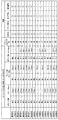
- 10 is a table summarizing conditions and evaluation results of Examples 1 to 8 and Comparative Examples 1 to 9.
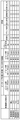
- 10 is a table summarizing conditions and evaluation results of Examples 5 and 9 to 11. It is the table
- FIG. It is the table
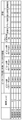
- FIG. 10 is a table summarizing the conditions and evaluation results of Examples 16 to 19.
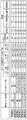
- 10 is a table summarizing the conditions and evaluation results of Examples 9 and 20 to 24.
- NMR Nuclear Magnetic Resonance
- a compound containing silicon as a main component is represented by the following formula: SiO 2 ⁇ nH 2 O.
- oxygen atoms O are bonded to each vertex of a tetrahedron of silicon atoms Si, and these oxygens It has a structure in which silicon atom Si is further bonded to atom O and spreads in a net shape.
- the schematic diagram shown below represents the Si—O net structure, ignoring the tetrahedral structure, but one of the oxygen atoms O in the Si—O—Si—O— repeating unit. Some of them are substituted with other members (for example, —H, —CH 3, etc.).
- These oxygen atoms are 4 bonded silicon atoms (i.e., silicon corresponding to Q n compounds) are generally collectively referred to as Q sites.
- Q 0 to Q 4 peaks derived from the Q site are referred to as a Q n peak group.
- the Q n peak group of the silica film containing no organic substituent is usually observed as a multimodal peak continuous in the region of ⁇ 80 to ⁇ 130 ppm chemical shift.
- each peak derived from the T site is observed as each peak of T 0 to T 3 as in the case of the Q site.
- each peak derived from the T site is referred to as a Tn peak group.
- the T n peak group is generally observed as a multimodal peak continuous in a region on the higher magnetic field side (usually chemical shift of ⁇ 80 to ⁇ 40 ppm) than the Q n peak group.
- the other (usually carbon) atoms are two bonded to are silicon atoms (i.e., silicon corresponding to D n compounds) are generally collectively referred to as D sites.
- D sites silicon atoms (i.e., silicon corresponding to D n compounds) are generally collectively referred to as D sites.
- D n peak group the peak derived from the D site is also observed as each peak of D 0 to D n (D n peak group), which is further than the peak group of Q n and T n. It is observed as a multimodal peak in the region on the high magnetic field side (usually the region with a chemical shift of ⁇ 3 to ⁇ 40 ppm).
- a silicon atom bonded with one oxygen atom and three other atoms is generally referred to as an M site, and is the region on the highest magnetic field side. It is observed as a multimodal peak (normally chemical shift 0 to -3 ppm).
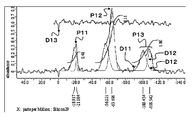
- FIG. 1A and FIG. 1B show an example of a solid-state Si-NMR spectrum.
- the horizontal axis of FIGS. 1A and 1B indicates the chemical shift, and the vertical axis indicates “relative strength” depending on the abundance of the compound having each structure.
- the measurement result shown in FIG. 1A is a measurement result for a sealing material for a light-emitting device containing silicon as a main component and indicating the presence of each of the D n peak group, the T n peak group, and the Q n peak group.
- D11 indicates actual measurement data
- D12 indicates data modeled by a Gaussian function.
- D13 indicates a difference spectrum.
- peaks P11, P12, and P13 are detected.
- the peak P11 has a peak top in the vicinity of a chemical shift of ⁇ 20.0 ppm. That is, the peak P11 indicates that it contains D n compounds.
- the width of the portion where the relative intensity is 1 ⁇ 2 of the peak value (that is, the half-value width) is about 10 ppm.
- waveform separation (peak separation) of the Si-NMR spectrum is performed by fitting using a Gaussian function or Lorentz function, and the relative intensity of each separated peak is 1 ⁇ 2 of the peak value.
- the width of the part to be is derived as the half width.
- Peak P12 has a peak top near the chemical shift of ⁇ 60.0 ppm. That is, the peak P12 indicates that it contains T n compounds. The full width at half maximum of this peak P12 is about 15 ppm.
- peak P13 has a peak top in the vicinity of a chemical shift of ⁇ 100.0 to ⁇ 110 ppm. That is, the peak P13 indicates that it contains Q n compounds. The half width of the peak P13 is about 17 ppm. Examples of such, FIG. 1A shows that it contains D n compound, T n compound, and Q n compounds.
- the measurement result shown in FIG. 1B is a measurement result for a sealing material for a light-emitting device whose main component is silicon indicating the presence of each of the T n peak group and the Q n peak group.
- D21 represents actual measurement data
- D22 represents data optimized by a Gaussian function.
- D23 indicates a difference spectrum.
- peaks P22 and P23 are detected.
- the peak P22 is a peak derived from the T site
- the peak P23 is a peak derived from the Q site.
- the half width of the peak P22 is about 15 ppm
- the half width of the peak P23 is about 17 ppm.
- the peak originating in D site is not detected. Therefore, the example of FIG. 1B includes a T n compound, and Q n compound, indicates that it does not contain a D n compound.
- the area ratio of the respective peak groups of D n , T n , and Q n is equal to the molar ratio of silicon atoms placed in the environment corresponding to each peak group. Therefore, if the area of all peaks with a molar amount of all silicon atoms, Q n peak group, T n peak group, the total area of the D n peak group and M n peak group is generally directly the carbon atom corresponding to these This corresponds to the molar amount of all silicon bonded.
- Emitting element encapsulating material according to the present invention has a Q n peak group half width is 5ppm or 12ppm or less, and T n peak group half width is 5ppm or 12ppm or less.
- Q n peak group half width is 5ppm or 12ppm or less
- T n peak group half width is 5ppm or 12ppm or less.
- the position of the peak top of the Q n peak group is present in the following areas chemical shift -120ppm than -90 ppm.
- the position of the peak top of the T n peak group is present in the following areas chemical shift -80ppm than -40 ppm.
- each peak group When there are a plurality of peaks in each peak group, as described above, the peaks are separated into a plurality of peaks by fitting using a Gaussian function or a Lorentz function, and the condition is determined for each peak. In addition, it is preferable that each of these peaks satisfy
- the sealing agent for light emitting elements of this invention is used for film-forming of the sealing layer for sealing a light emitting element. What hardened the sealing agent for light emitting elements of this invention can be used as a sealing material for light emitting elements.
- the cured film (sealing layer) of the sealing agent for light emitting device of the present invention has good adhesion to the light emitting device and also has high resistance to sulfur gas.
- the cured film is excellent in transparency, light resistance and heat resistance even when it is a thick film, and does not cause cracks even when used for a long time. The mechanism for obtaining such characteristics is considered as follows.
- the sealing agent for light emitting device of the present invention includes polysiloxane having a certain degree of cross-linking to which a trifunctional silane compound and a tetrafunctional silane compound are polymerized.
- the tetrafunctional silane compound has many bonds, and reacts effectively with the OH group of the metal reflection layer or the resin part to form a covalent bond, thereby exhibiting high adhesion.
- the crosslink density is also increased, it is difficult to permeate sulfide gas or water vapor. As a result, an effect of suppressing corrosion deterioration of the metal reflective layer or the like is exhibited.
- the trifunctional silane compound has an effect of imparting flexibility to the sealing agent layer for a light emitting element by an organic group such as a methyl group and suppressing cracks derived from the high crosslink density of the tetrafunctional silane compound.
- the highly functional tetrafunctional silane compound present in the vicinity of the surface of the light emitting device is first replaced by the trifunctional silane compound. Also effectively forms a covalent bond with the OH group on the surface of the light emitting element, creating a ground that leads to high adhesion.
- the crosslink density is higher, and it is difficult for sulfurized gas and water vapor to pass therethrough.
- an unreacted group of the tetrafunctional silane compound bonded to the surface of the light emitting element forms a bond with the remaining tetrafunctional silane compound and the trifunctional silane compound, thereby forming a sealing material layer for the light emitting element.
- the trifunctional silane compound is polymerized more at a distance from the interface with the light emitting element due to its reactivity, flexibility is imparted to the sealing material layer for the light emitting element and cracks are less likely to occur.
- the unreacted tetrafunctional silane compound promotes the crosslinking of the light-emitting element sealing material layer, gas barrier properties such as sulfur gas and water vapor are also improved.
- the sealing material for a light emitting device of the present invention achieves both adhesion capable of withstanding a thermal shock and crack resistance.
- the sealing material for light emitting elements which originates in the thermal degradation and light degradation of an organic group by using the bifunctional silane compound component with many organic groups below predetermined amount.
- the encapsulant for light emitting devices of the present invention contains no phosphor particles (referred to as “binder-type encapsulant”) and contains phosphor-containing particles (referred to as “phosphor-containing encapsulant”). ).
- Binder-type sealant contains polysiloxane, an organometallic compound, and a solvent, and contains inorganic fine particles as necessary.
- Polysiloxane is a polymer obtained by hydrolyzing and polycondensing a silane compound represented by the following general formula (I) or an oligomer thereof.
- OR 1 represents a hydrolyzable group
- Y represents a monovalent organic group
- m represents an integer of 1 to 4.
- OR 1 represents a hydrolyzable group.
- the hydrolyzable group refers to a group that is hydrolyzed with water in a binder-type sealant to generate a hydroxyl group rich in reactivity.
- Examples of the hydrolyzable group include a lower alkoxy group having 1 to 5 carbon atoms, an acetoxy group, a butanoxime group, a chloro group and the like.
- One of these hydrolyzable groups may be contained alone, or two or more thereof may be contained.
- the hydrolyzable group is preferably a lower alkoxy group having 1 to 5 carbon atoms, more preferably a methoxy group or an ethoxy group, since the component liberated after the reaction is neutral.
- Y represents a monovalent organic group.
- the monovalent organic group represented by Y include groups known as monovalent organic groups of so-called silane coupling agents. Specifically, the aliphatic group, alicyclic group, aromatic group, alicyclic group having 1 to 1000 carbon atoms, preferably 500 or less, more preferably 100 or less, further preferably 50 or less, and particularly preferably 6 or less. Represents an aromatic group. These may have atoms or atomic groups such as O, N, and S as a linking group.
- the monovalent group represented by Y is preferably a methyl group from the viewpoint that the light resistance and heat resistance of the cured film of the binder-type sealant can be improved.
- the organic group represented by Y in the above general formula (I) may have a substituent.
- Substituents are, for example, atoms such as F, Cl, Br, I; vinyl group, methacryloxy group, acryloxy group, styryl group, mercapto group, epoxy group, epoxycyclohexyl group, glycidoxy group, amino group, cyano group, nitro group
- an organic functional group such as a sulfonic acid group, a carboxy group, a hydroxy group, an acyl group, an alkoxy group, an imino group, and a phenyl group.
- m represents an integer of 1 to 4.
- m 1, it is a monofunctional silane compound.
- the polysiloxane contained in the sealing agent of the present invention needs to contain a polymer of at least a trifunctional silane compound and a tetrafunctional silane compound.
- the trifunctional silane compound includes a compound represented by the following general formula (II). Si (OR 1 ) 3 CH 3 (II)
- each R 1 independently represents an alkyl group or a phenyl group, and preferably represents an alkyl group having 1 to 5 carbon atoms or a phenyl group.
- the trifunctional silane compound corresponds to T n compounds described above.
- the trifunctional silane compound examples include methyltrimethoxysilane, methyltriethoxysilane, methyltripropoxysilane, methyltripentyloxysilane, methylmonomethoxydiethoxysilane, methylmonomethoxydipropoxysilane, and methylmonomethoxydipentyl.
- Oxysilane, methylmonomethoxydiphenyloxysilane, methylmethoxyethoxypropoxysilane, methylmonomethoxymonoethoxymonobutoxysilane and the like are included.
- methyltrimethoxysilane and methyltriethoxysilane are preferable, and methyltrimethoxysilane is more preferable.
- Examples of the tetrafunctional silane compound include a compound represented by the following general formula (III). Si (OR 2 ) 4 (III) In the general formula (III), each R 2 independently represents an alkyl group or a phenyl group, preferably an alkyl group having 1 to 5 carbon atoms, or a phenyl group.
- the tetrafunctional methylsilane compound corresponds to Q n compounds described above.
- Y 4-4 Y 0 in the formula (I) indicates that no monovalent organic group is contained.
- tetrafunctional silane compounds include tetramethoxysilane, tetraethoxysilane, terapropoxysilane, tetrabutoxysilane, tetrapentyloxysilane, tetraphenyloxysilane, trimethoxymonoethoxysilane, dimethoxydiethoxysilane, triethoxymono.
- Sealing agent for light-emitting element according to the present invention in a solid Si-NMR spectrum, it has a Q n peak group half width is 5ppm or 12ppm or less, and T n peak group half width is 5ppm or 12ppm or less .
- the Q n peak group is derived from a Q n compound, that is, a tetrafunctional silane compound
- the T n peak group is derived from a T n compound, that is, a trifunctional monomethylsilane compound. Therefore, the polysiloxane according to the present embodiment polymerizes the trifunctional monomethylsilane compound and the tetrafunctional silane compound so as to satisfy the above conditions.
- the molar ratio of silicon corresponding to the Q n compound to the total silicon is 25% or more and 60% or less, and the molar ratio of silicon corresponding to the T n compound is 25 Polymerization is performed so as to be not less than 60% and not more than 60%. At this time, the molar ratio of silicon corresponding to D n compound is desirably less than 30%.
- a sealing agent and the coating object light emitting element A covalent bond with a certain light-emitting device for example, a metal reflector or a package
- adhesion that can withstand a thermal shock is not exhibited.
- the crosslink density becomes low and deterioration of the metal reflective layer due to the permeation of corrosive gas or the like cannot be suppressed.
- a crosslinking density will be too high and it will become easy to enter a crack.
- the molar ratio of silicon corresponding to T n compound is smaller than the above range, flexibility of the light-emitting element sealing agents according to the present invention is insufficient, it is impossible to suppress the crack.
- the covalent bond between the light-emitting element sealant and the light-emitting device that is an object to be coated is insufficient, and adhesion that can withstand thermal shock does not appear.
- the Tn compound is trifunctional and can form a covalent bond with each part of the light emitting device (for example, a metal reflector or a package) to some extent, like a tetrafunctional Qn compound. This is probably because the bond is not sufficient.
- the molar ratio of silicon corresponding to D n compound is 30% or more, cracking resistance by flexibility is improved, a sealant and the coating object light emitting element emitting device (e.g., Ya metallic reflecting plate Insufficient covalent bond with the package), and adhesion that can withstand thermal shock is not exhibited.
- the D n compound is bifunctional, it has lower adhesion than the T n compound. Also, the lower the crosslink density is derived from the presence of D n compound, no longer possible to suppress the deterioration of the metal reflecting layer by transmission of corrosive gases. Furthermore, D n compounds for become more functional groups derived from organic matter that changes color with heat, leads to a decrease in heat resistance.
- Emitting element encapsulating material according to the present invention includes both at least Q n compound and T n compound within a range described above. By setting it as such a composition, the sealing material for light emitting elements which is excellent in adhesiveness, crack tolerance, and gas-barrier property can be obtained.
- the encapsulant for light emitting device has a silanol content of usually 11% to 30%, preferably 20% to 25%. Adjustment of the silanol content of the light emitting device encapsulant within the same range can be achieved by polymerizing a mixture of a tetrafunctional silane compound and a trifunctional silane compound at a predetermined ratio. it can. At this time, a bifunctional silane compound may be mixed within a range where the silanol content of the sealing material for a light emitting device does not exceed 11% or more and 30% or less.
- the sealing material using the light emitting layer has a silicon content of 20% by weight or more.
- silicone resin light emitting device sealing materials such as epoxy resins
- silicone-based sealants for light-emitting elements formed with a skeleton in which siloxane bonds are three-dimensionally bonded with a high degree of crosslinking are made of glass or rock. It is close to inorganic materials such as. Therefore, it can be understood that the protective film is rich in heat resistance and light resistance.
- a sealant for a silicone-based light-emitting element having a methyl group as a substituent has no absorption in the ultraviolet region, so that photolysis hardly occurs and has excellent light resistance.
- the silicon content of the sealant for a light emitting device according to the present invention is 20% by weight or more, preferably 25% by weight or more, and more preferably 30% by weight or more.
- the upper limit is usually in the range of 47% by weight or less because the silicon content of the glass composed solely of SiO 2 is 47% by weight.
- the silicon content rate of the sealing material for light emitting elements which concerns on this invention can be controlled by selection of the monovalent organic group represented by Y in the general formula (I) mentioned above.
- the silicon content of the encapsulant for a semiconductor light-emitting device of the present invention 20% by weight or more, it can be achieved by setting the monovalent organic group represented by Y to 6 or less carbon atoms.
- the monovalent group represented by Y is preferably a methyl group.
- the silicon content of the light-emitting element sealing material can be calculated based on, for example, inductively coupled plasma spectroscopy (hereinafter abbreviated as “ICP” as appropriate) analysis. it can.
- ICP inductively coupled plasma spectroscopy
- the silanol content of the semiconductor light emitting device member is measured by, for example, a solid Si-NMR spectrum, and the ratio of the peak area derived from silanol to the total peak area is the silicon atom that is silanol in the total silicon atoms. The ratio (%) of is calculated. This can be calculated by comparing with the separately analyzed silicon content.
- the polymerization ratio of the trifunctional monomethylsilane compound and the tetrafunctional silane compound is not particularly limited as long as the above-described conditions are satisfied.
- the molar ratio of the tetrafunctional silane compound is excessive, the degree of cross-linking of the polysiloxane becomes large when forming a cured film. Therefore, the shrinkage amount of the cured film increases and cracks are likely to occur.
- the molar ratio of the functional monomethylsilane compound is excessive, the amount of trifunctional monomethylsiloxane-derived methyl groups (organic groups) in the cured film increases. As a result, liquid repellency is likely to occur when the binder-type sealant is applied.
- the degree of cross-linking of the polysiloxane is reduced, the resistance to sulfur gas tends to be reduced.
- the polymerization ratio may be determined in consideration of these characteristics.
- the mass average molecular weight of the polysiloxane is 1000 to 3000, preferably 1200 to 2700, and more preferably 1500 to 2000.
- the mass average molecular weight is less than 1000, the viscosity is low and liquid repellency or the like is likely to occur.
- the mass average molecular weight exceeds 3000, the viscosity increases and it may be difficult to form a uniform film. Moreover, the embedding property of the light emitting element may be poor.
- the mass average molecular weight is a value (polystyrene conversion) measured by gel permeation chromatography.
- Polysiloxane is prepared by hydrolyzing the above-mentioned trifunctional monomethylsilane compound and tetrafunctional silane compound in the presence of an acid catalyst, water, and an organic solvent, followed by a condensation reaction.
- the mass average molecular weight of the resulting polysiloxane can be adjusted by reaction conditions (particularly reaction time) and the like.
- a trifunctional monomethylsilane compound and a tetrafunctional silane compound may be preliminarily mixed in the above molar ratio and polymerized randomly.
- the polymer may be polymerized in blocks, such as by polymerizing only the tetrafunctional silane compound.
- the acid catalyst added during the polymerization of the trifunctional monomethylsilane compound and the tetrafunctional silane compound may be any compound that hydrolyzes the silane compound in the presence of water, and may be either an organic acid or an inorganic acid.
- inorganic acids include sulfuric acid, phosphoric acid, nitric acid, hydrochloric acid, etc. Among them, phosphoric acid and nitric acid are preferable.
- organic acids include formic acid, oxalic acid, fumaric acid, maleic acid, glacial acetic acid, acetic anhydride, propionic acid, n-butyric acid and other carboxylic acid residues, and organic sulfonic acid and other sulfur-containing acid residues. The compound which has is included.
- Specific examples of the organic acid include organic sulfonic acid or esterified products thereof (organic sulfate ester, organic sulfite ester).
- an organic sulfonic acid represented by the following general formula (IV) is particularly preferable.
- R 3 —SO 3 H (IV) (In general formula (IV), R 3 is a hydrocarbon group which may have a substituent.)
- the hydrocarbon group represented by R 3 may be a linear, branched, or cyclic hydrocarbon group having 1 to 20 carbon atoms.
- the hydrocarbon may be a saturated hydrocarbon or an unsaturated hydrocarbon.
- it may have a substituent such as a halogen atom such as a fluorine atom, a sulfonic acid group, a carboxyl group, a hydroxyl group, an amino group, or a cyano group.
- examples of the cyclic hydrocarbon group represented by R 3 include an aromatic hydrocarbon group such as a phenyl group, a naphthyl group, or an anthryl group, and particularly preferably a phenyl group.
- the aromatic hydrocarbon group may have a linear, branched, or cyclic saturated or unsaturated hydrocarbon group having 1 to 20 carbon atoms as a substituent.
- the organic sulfonic acid represented by the general formula (IV) is preferably nonafluorobutanesulfonic acid, methanesulfonic acid, trifluoromethanesulfonic acid, dodecylbenzenesulfonic acid or a mixture thereof.
- the amount of the acid catalyst to be mixed at the time of preparing the polysiloxane is preferably such that the concentration of the acid catalyst in the system in which the hydrolysis reaction of the silane compound is performed is 1 to 1000 ppm, more preferably in the range of 5 to 800 ppm.
- the film quality and storage stability of polysiloxane vary depending on the amount of water mixed during preparation of polysiloxane. Therefore, the water addition rate is adjusted according to the target film quality and the like.
- the water addition rate is the ratio (%) of the number of moles of water molecules to be added to the number of moles of alkoxy groups of the silane compound added to the reaction system for preparing the polysiloxane.
- the water addition rate is preferably 50 to 200%, more preferably 75 to 180%.
- the water addition rate is preferably 50 to 200%, more preferably 75 to 180%.
- solvents used in the preparation of polysiloxanes include monohydric alcohols such as methanol, ethanol, propanol and n-butanol; alkyl carboxylic acids such as methyl-3-methoxypropionate and ethyl-3-ethoxypropionate Esters; polyhydric alcohols such as ethylene glycol, diethylene glycol, propylene glycol, glycerin, trimethylolpropane, hexanetriol; ethylene glycol monomethyl ether, ethylene glycol monoethyl ether, ethylene glycol monopropyl ether, ethylene glycol monobutyl ether, diethylene glycol monomethyl ether, Diethylene glycol monoethyl ether, diethylene glycol monopropyl ether, diethylene glycol monobutyl Ethers, propylene glycol monomethyl ether, propylene glycol monoethyl ether, propylene glycol monopropyl ether, monoethers of polyhydric alcohols such
- Esters such as acetone, methyl ethyl ketone, methyl isoamyl ketone; ethylene glycol dimethyl ether, ethylene glycol diethyl ether, ethylene glycol dipropyl ether, ethylene glycol dibutyl ether, propylene glycol dimethyl ether, propylene glycol diethyl ether, diethylene glycol dimethyl ether, diethylene glycol diethyl ether , Diethylene Polyhydric alcohols ethers all hydroxyl groups of polyhydric alcohols such as call methyl ethyl ether was alkyletherified; and the like. These may be used alone or in combination of two or more.
- the binder-type sealant may contain an organometallic compound composed of a metal alkoxide or metal chelate containing a group 4 or group 13 metal element. As described above, the metal in the organometallic compound forms a metalloxane bond with polysiloxane and the hydroxyl group of each member of the light-emitting element. Part of the organometallic compound forms a nano-sized cluster composed of siloxane bonds in the cured film of the binder-type sealant.
- the organometallic compound is preferably a compound represented by the following general formula (V).
- M m + X n Y mn (V)
- M represents a group 4 or group 13 metal element.
- m represents the valence of M and represents 3 or 4.
- n represents the number of X groups and is an integer of 2 or more and 4 or less. However, m ⁇ n.
- the metal element represented by M is preferably aluminum, zirconium, or titanium, and particularly preferably zirconium.
- Zirconium metal alkoxides or metal chelates do not have an absorption wavelength in the emission wavelength region of a general light-emitting element (particularly blue light (wavelength 420 nm to 485 nm)). Therefore, the cured film containing a zirconium-based metal element transmits light emitted from the light emitting element without absorbing it, and the light extraction property is improved.
- X represents a hydrolyzable group.
- the hydrolyzable group refers to a group that is hydrolyzed with water in a binder-type sealant to generate a hydroxyl group rich in reactivity.
- Examples of the hydrolyzable group include a lower alkoxy group having 1 to 5 carbon atoms, an acetoxy group, a butanoxime group, a chloro group and the like.
- One of these hydrolyzable groups may be contained alone, or two or more thereof may be contained.
- the hydrolyzable group is preferably a lower alkoxy group having 1 to 5 carbon atoms, more preferably a methoxy group or an ethoxy group, since the component liberated after the reaction is neutral.
- Y represents a monovalent organic group.
- the monovalent organic group represented by Y include groups known as monovalent organic groups of so-called silane coupling agents. Specifically, the aliphatic group, alicyclic group, aromatic group, alicyclic group having 1 to 1000 carbon atoms, preferably 500 or less, more preferably 100 or less, further preferably 50 or less, and particularly preferably 6 or less. Represents an aromatic group. These may have atoms or atomic groups such as O, N, and S as a linking group.
- the monovalent group represented by Y is preferably a methyl group from the viewpoint that the light resistance and heat resistance of the cured film of the binder-type sealant can be improved.
- the organic group represented by Y in the general formula (V) may have a substituent.
- Substituents are, for example, atoms such as F, Cl, Br, I; vinyl group, methacryloxy group, acryloxy group, styryl group, mercapto group, epoxy group, epoxycyclohexyl group, glycidoxy group, amino group, cyano group, nitro group
- an organic functional group such as a sulfonic acid group, a carboxy group, a hydroxy group, an acyl group, an alkoxy group, an imino group, and a phenyl group.
- organometallic compound represented by the general formula (V) include the following compounds.
- metal alkoxide or metal chelate containing aluminum element include aluminum triisopropoxide, aluminum tri-n-butoxide, aluminum tri-t-butoxide, aluminum triethoxide and the like.
- metal alkoxides or metal chelates containing elemental zirconium examples include zirconium tetramethoxide, zirconium tetraethoxide, zirconium tetra n-propoxide, zirconium tetra i-propoxide, zirconium tetra n-butoxide, zirconium tetra i-butoxide, Zirconium tetra-t-butoxide, zirconium dimethacrylate dibutoxide, dibutoxyzirconium bis (ethylacetoacetate) and the like.
- metal alkoxides or metal chelates containing elemental titanium include titanium tetraisopropoxide, titanium tetra n-butoxide, titanium tetra i-butoxide, titanium methacrylate triisopropoxide, titanium tetramethoxypropoxide, titanium tetra n-propoxy. , Titanium tetraethoxide, titanium lactate, titanium bis (ethylhexoxy) bis (2-ethyl-3-hydroxyhexoxide), titanium acetylacetonate, and the like.
- the compounds exemplified above are some of the commercially available organometallic compounds that are readily available, and are listed in the coupling agent and related products list in Chapter 9 of “Optimum Utilization Technology for Coupling Agents” published by the Science and Technology Research Institute.
- the compounds shown can also be applied to the present invention as the organometallic compounds.
- the organometallic compound is preferably added in an amount of 5 to 100 parts by mass, more preferably 8 to 40 parts by mass, and still more preferably 10 to 15 parts by mass with respect to 100 parts by mass of the polysiloxane. If the amount is less than 5 parts by mass, the effect of adding the organometallic compound cannot be obtained. On the other hand, when it exceeds 100 mass parts, the preservability of a binder type sealing agent will fall.
- the binder type sealant contains a solvent.
- the solvent may be an aqueous solvent in which water and an organic solvent excellent in water compatibility are combined, or an organic solvent having low water compatibility and not containing water.
- Examples of the organic solvent having excellent compatibility with water include alcohols such as methanol, ethanol, propanol, and butanol.
- the binder-type sealant of the present invention preferably contains an aqueous solvent, that is, water.
- the amount of water contained in the binder-type sealant is preferably 10 to 120 parts by mass, more preferably 80 to 100 parts by mass with respect to 100 parts by mass of the polysiloxane.
- the binder-type sealant is preferably 10 to 120 parts by mass, more preferably 80 to 100 parts by mass with respect to 100 parts by mass of the polysiloxane.
- the polysiloxane can be sufficiently hydrolyzed, and the heat resistance and the like of the cured film are sufficient.
- hydrolysis or the like may occur during storage of the binder-type sealant.
- the solvent for the binder-type sealant includes an organic solvent having a boiling point of 150 ° C. or higher, such as ethylene glycol or propylene glycol.
- an organic solvent having a boiling point of 150 ° C. or higher is contained, the storage stability of the binder-type sealant is improved.
- an organic solvent having a boiling point of 150 ° C. or higher is contained, it can be easily discharged from the discharge port of the discharge device when the binder-type sealant is applied.
- the boiling point of the solvent is preferably 250 ° C. or lower. This is because the drying property of the binder-type sealant can be improved.
- the binder type sealant may contain inorganic fine particles.
- inorganic fine particles By including inorganic fine particles, the thickening effect of the binder-type sealant can be obtained. Furthermore, the strength of the cured film of the binder-type sealant is improved. Further, when inorganic fine particles having a high refractive index are contained, the light extraction efficiency of the cured film of the binder-type sealant is increased.
- inorganic fine particles examples include oxide fine particles such as zirconium oxide, silicon oxide, titanium oxide, and zinc oxide (that is, inorganic oxide fine particles) and fluoride fine particles such as magnesium fluoride.
- the average particle size of the inorganic fine particles is preferably 1 nm or more and 50 ⁇ m or less in consideration of the respective effects described above.
- the average particle diameter of the inorganic fine particles is measured, for example, by a Coulter counter method.
- the inorganic fine particles are preferably porous, and the specific surface area is preferably 200 m 2 / g or more. If the inorganic fine particles are porous, the solvent enters the porous voids, and the viscosity of the binder-type sealant is effectively increased. However, the viscosity of the binder-type sealing material is not simply determined by the amount of the porous inorganic fine particles, but varies depending on the ratio between the inorganic fine particles and the solvent, the amount of other components, and the like.
- the amount of inorganic fine particles in the binder-type sealant is preferably such that the amount of inorganic fine particles in the cured product of the binder-type sealant is 0.5% by mass or more and 50% by mass or less, more preferably 1 to 40. % By mass.
- the amount of the inorganic fine particles is less than 0.5% by mass, the above-described thickening effect and the effect of improving the strength of the cured film cannot be obtained. Moreover, when it exceeds 50 mass%, the intensity
- the surface of the inorganic fine particles may be treated with a silane coupling agent or a titanium coupling agent. By the surface treatment, compatibility between the inorganic fine particles and the polysiloxane or the solvent is increased.
- the binder type sealant preferably has a pH of 1 to 4. When the pH is less than 1 or exceeds 4, the polysiloxane or the organometallic compound may react and precipitates may be generated during storage.
- a pH adjuster such as nitric acid may be included as necessary.
- the viscosity of the binder-type sealant is preferably 10 to 1000 cP, more preferably 12 to 800 cP, and still more preferably 20 to 600 cP.
- the viscosity of the binder-type sealant is too low, the binder-type sealant flows when the binder-type sealant is applied, and the sealing layer cannot be applied to the target region.
- the viscosity of a binder type sealing agent is too high, application
- the viscosity can be adjusted by the amount of the inorganic fine particles described above.
- the binder-type sealant is prepared by mixing polysiloxane, an organometallic compound, and, if necessary, inorganic fine particles in a solvent. Stirring of the mixed liquid can be performed by an arbitrary method, and for example, can be performed using a stirring mill, a blade kneading stirring apparatus, a thin film swirling disperser, or the like.
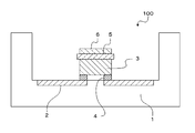
- the binder-type sealant is used for forming the sealing layer 7 of the LED device 100 as shown in the schematic cross-sectional view of FIG. 2C, for example.
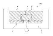
- the LED device 100 having the configuration further includes a phosphor-containing resin layer 8 that converts the wavelength of light emitted from the LED chip 3 on the sealing layer 7.
- the sealing layer 7 has a function of sealing the light emitting element package 1, the metal part 2, the LED chip 3, and the like.
- the sealing layer 7 is formed by applying a binder-type sealant so as to cover the package 1, the metal part 2, the LED chip 3, and the like of the light emitting element, and drying and curing this.
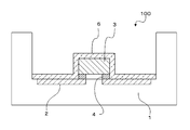
- the binder-type sealant is also used for forming the sealing layer 6 of the LED device 100 as shown in the schematic cross-sectional view of FIG. 2A, for example.
- the sealing layer 6 has not only a sealing function for the LED chip 3 and the metal part 2 but also a wavelength conversion function for converting the wavelength of light emitted from the LED chip 3.
- the sealing layer 6 in the LED device 100 has phosphor particles arranged in advance on a glass substrate 5 for protecting the package 1, the metal part 2, and the LED chip 3, and a binder type on the phosphor particles. It is obtained by applying a sealant, drying and curing. That is, the sealing layer 6 containing phosphor-containing particles is formed inside the layer by forming the film by this method.
- the phosphor-containing sealant includes polysiloxane, organometallic compound, solvent, and phosphor particles, and includes tabular particles, inorganic fine particles, and the like as necessary.
- the polysiloxane contained in the phosphor-containing sealant can be the same as the polysiloxane contained in the binder-type sealant described above.
- the amount of polysiloxane contained in the phosphor-containing sealant is preferably such that the amount of polysiloxane in the cured product of the phosphor-containing sealant is 3% by mass or more and 35% by mass or less, and 10% by mass or more and 30% by mass. % Is preferred.
- the polysiloxane functions as a binder in the cured product of the phosphor-containing sealant, if the amount of the binder is less than 3% by mass, a cured film having sufficient coating strength cannot be obtained. On the other hand, when the amount of polysiloxane exceeds 35% by mass, the content of phosphor particles, tabular particles and the like is relatively lowered, and the viscosity of the phosphor-containing encapsulant is likely to be lowered.
- the organometallic compound contained in the phosphor-containing encapsulant can be the same as the organometallic compound contained in the binder-type encapsulant.
- the amount of the organometallic compound relative to the amount of polysiloxane can be the same as that of the binder-type sealant described above.
- the solvent contained in the phosphor-containing encapsulant is an aqueous solvent that combines water and an organic solvent that is excellent in water compatibility, or an organic solvent that has low water compatibility and does not contain water. Any of non-aqueous solvents may be used. However, when the phosphor particles contained in the phosphor-containing sealant are easily deteriorated by water, a non-aqueous solvent is preferable.
- an aqueous solvent is preferable as described above.
- hydrolysis of polysiloxane is promoted.
- tabular particles, fluoride particles and the like can be swollen, and the viscosity of the phosphor-containing sealant is increased.
- impurities are contained in water, swelling of tabular grains and the like may be inhibited. Therefore, it is desirable that the water contained in the phosphor-containing sealant does not contain impurities.
- the phosphor particles may be any particles that are excited by the wavelength (excitation wavelength) of light emitted from the light emitting element (LED chip) and emit fluorescence having a wavelength different from the excitation wavelength.
- a white LED element is obtained by including phosphor particles that emit yellow fluorescence.
- the phosphor particles that emit yellow fluorescence include YAG (yttrium, aluminum, garnet) phosphors.
- the YAG phosphor can convert blue light (wavelength 420 nm to 485 nm) emitted from the blue LED element into yellow light (wavelength 550 nm to 650 nm).
- the phosphor particles are, for example, 1) an appropriate amount of a fluoride such as ammonium fluoride is mixed and pressed into a mixed raw material having a predetermined composition to obtain a molded body, and 2) the obtained molded body is put into a crucible. It can be produced by packing and firing in air at a temperature range of 1350 to 1450 ° C. for 2 to 5 hours to obtain a sintered body.
- a fluoride such as ammonium fluoride
- a mixed raw material having a predetermined composition is obtained by sufficiently mixing the oxides of Y, Gd, Ce, Sm, Al, La, and Ga, or compounds that easily become oxides at high temperatures in a stoichiometric ratio. Can do.
- the mixed raw material having a predetermined composition may be prepared by coprecipitation with a solution obtained by dissolving a rare earth element of Y, Gd, Ce, and Sm in a stoichiometric ratio with an oxalic acid, and oxidation. It can be obtained by mixing aluminum and gallium oxide.
- the kind of the phosphor is not limited to the YAG phosphor, and other phosphors such as a non-garnet phosphor not containing Ce may be used.
- the average particle diameter of the phosphor particles is preferably 1 ⁇ m or more and 50 ⁇ m or less, and more preferably 10 ⁇ m or less.
- the larger the particle size of the phosphor particles the higher the light emission efficiency (wavelength conversion efficiency).
- the particle diameter of the phosphor particles is too large, a gap generated at the interface between the phosphor particles and polysiloxane becomes large. Thereby, the intensity
- the average particle diameter of the phosphor particles can be measured, for example, by a Coulter counter method.
- the amount of phosphor particles contained in the phosphor-containing encapsulant is preferably such that the amount of phosphor particles in the cured film of the phosphor-containing encapsulant is 60 to 95% by mass. Basically, the higher the concentration of the phosphor particles in the cured film of the phosphor-containing sealant, the better. As the concentration of the phosphor particles increases, the binder content decreases, and the distribution of the phosphor particles in the cured film tends to be uniform. Moreover, if the density
- the concentration of the phosphor particles in the cured film of the phosphor-containing sealant is high, the phosphor particles are brought into close contact with each other, so that the strength of the cured film of the phosphor-containing sealant is increased. Furthermore, when the concentration of the phosphor particles in the cured film is high, heat generated from the phosphor particles is easily dissipated from the cured film.
- the concentration of the phosphor particles in the cured film of the phosphor-containing sealant is too high (greater than 95% by mass), the binder content is extremely reduced, and the phosphor particles are bound to each other. You may not be able to.
- the concentration of the phosphor particles in the cured film can be determined from the amount of phosphor particles added to the phosphor-containing sealant.
- the phosphor-containing sealant may contain tabular grains together with the phosphor particles.
- the phosphor-containing encapsulant contains tabular particles, the viscosity of the phosphor-containing encapsulant increases, and sedimentation of the phosphor particles in the encapsulant is suppressed.
- the tabular grains exist as a card house structure in the phosphor-containing sealant, and the viscosity of the sealant is significantly increased with a small amount.
- a typical example of the tabular particles contained in the phosphor-containing sealant is layered clay mineral fine particles.
- the main component of the layered clay mineral fine particles is a layered silicate mineral, preferably a swellable clay mineral having a mica structure, a kaolinite structure, a smectite structure, etc., and a swellable clay mineral having a smectite structure rich in swelling properties. More preferred. Since the layered clay mineral fine particles have a flat plate shape, the film strength of the ceramic layer constituting the phosphor-containing sealant can also be improved.
- the content of the tabular particles is preferably such that the amount of the tabular particles in the cured film of the phosphor-containing encapsulant is 0.5% by mass or more and 20% by mass or less, and 0.5% by mass or more and 10% by mass or less. Is more preferred. If the content of tabular grains in the cured film is less than 0.5% by mass, the effect of adding tabular grains cannot be sufficiently obtained. On the other hand, when the content of the layered silicate mineral exceeds 20% by mass, the strength of the phosphor-containing sealant is lowered.
- the surface of the layered clay mineral fine particles may be modified (surface treatment) with an ammonium salt or the like in consideration of compatibility with the solvent.
- the phosphor-containing sealant may contain inorganic fine particles.
- the inorganic fine particles enter the gaps between the phosphors, and the strength of the cured film of the phosphor-containing sealing agent is increased. Further, when the inorganic fine particles are porous, the solvent enters the porous voids, and the viscosity of the phosphor-containing sealing agent is effectively increased.
- the specific surface area of the inorganic fine particles is preferably 200 m 2 / g or more.
- inorganic fine particles include fine oxide particles such as zirconium oxide, silicon oxide, titanium oxide, and zinc oxide, and fine fluoride particles such as magnesium fluoride.
- the average particle size of the inorganic fine particles contained in the phosphor-containing sealant is preferably 1 nm or more and 50 ⁇ m or less, more preferably 1 nm to 10 ⁇ m, and further preferably 1 nm to 100 nm in consideration of the respective effects described above.
- the average particle diameter of the inorganic fine particles can be measured, for example, by a Coulter counter method.
- the amount of inorganic fine particles contained in the phosphor-containing sealant is preferably such that the amount of inorganic fine particles in the cured product of the phosphor-containing sealant is 0.5% by mass or more and 50% by mass or less. 1 to 40% by mass.
- the amount of the inorganic fine particles is less than 0.5% by mass, the gap between the phosphor particles cannot be filled with the inorganic fine particles, and the above-described thickening effect and film strength improving effect cannot be obtained.
- the amount of the inorganic fine particles is less than 0.5% by weight, the phosphor particle component is relatively increased, so that the handling property at the time of applying the phosphor-containing sealant is lowered. Therefore, it becomes difficult to form a layer with uniform chromaticity.
- the amount of the inorganic fine particles exceeds 50% by mass, the inorganic fine particles excessively scatter the excitation light of the light emitting element, and the light extraction efficiency of the light emitting device decreases.
- the surface of the inorganic fine particles may be treated with a silane coupling agent or a titanium coupling agent. By the surface treatment, compatibility between the inorganic fine particles and the polysiloxane or the solvent is increased.
- the sealing agent for light emitting device may contain a cyclic ether compound.
- the ring of the cyclic ether compound can capture metal ions and the like. For this reason, the metal ion which flows out from the metal reflector etc. of a light-emitting device under wet heat can be captured, and the corrosion by metal migration can be suppressed.
- the cyclic ether compound contained in the sealant for a light emitting device may be a cyclic compound represented by the formula (VI). (—CH 2 —CH 2 —Z—) n (VI)
- n represents an integer of 1 or more.
- R represents hydrogen “H” or an alkylene group having 1 to 1000 carbon atoms.
- the cyclic ether compound may contain a benzene ring or the like as represented by the formula (VII). [Chemical 2]
- cyclic ether compound examples include 12-crown-4, 15-crown-5, 18-crown-6, 21-crown-7, dibenzo-18-crown-6, diaza-18-crown-6 and the like. Can be mentioned.
- the ring size is preferably from 15 to 21 members, more preferably 18 members.
- the content of the cyclic ether compound is preferably from 0.1 to 5.0% by mass, more preferably from 0.5 to 3.0% by mass, based on the total solid content of the sealant for a light-emitting device. More preferably, it is 1.0 to 2.0% by mass.
- the cyclic ether compound is contained in an amount of 0.1% by mass or more, the wet heat resistance of the cured film of the light-emitting device sealant tends to increase.
- the sealing agent for light emitting device may contain a silane coupling agent. Hydroxyl groups that are expressed by hydrolysis of the silane coupling agent are subjected to dehydration condensation reaction with hydroxyl groups present on the surface of the light emitting element to form siloxane bonds. The hydroxyl group also reacts with polysiloxane (first polysiloxane and second polysiloxane) to form a siloxane bond.
- the adhesion between the cured product of the light-emitting device sealant and the light-emitting element is further increased, and as a result, contact between water vapor and the light-emitting device is suppressed. Therefore, the resistance to wet heat is improved.
- the silane coupling agent contained in the light-emitting device sealant may be a compound represented by the following general formula (VIII). [Chemical formula 3]
- Y represents a divalent organic group
- X represents a hydrolyzable group
- R represents an alkylene group
- N represents an integer of 1 to 3.
- the divalent organic group represented by Y is a fat having 1 to 1000 carbon atoms, preferably 500 or less, more preferably 100 or less, still more preferably 50 or less, particularly preferably 6 or less. It can be an aromatic group, an alicyclic group, an aromatic group, or an alicyclic aromatic group. These may have atoms or atomic groups such as O, N, and S as a linking group.
- Y in the general formula (VIII) may have a substituent.
- Substituents are, for example, atoms such as F, Cl, Br, I; vinyl group, methacryloxy group, acryloxy group, styryl group, mercapto group, epoxy group, epoxycyclohexyl group, glycidoxy group, amino group, cyano group, nitro group
- an organic functional group such as a sulfonic acid group, a carboxy group, a hydroxy group, an acyl group, an alkoxy group, an imino group, and a phenyl group.
- X is a hydrolyzable group.
- the hydrolyzable group include a lower alkoxy group having 1 to 5 carbon atoms, an acetoxy group, a butanoxime group, a chloro group and the like.
- One of these hydrolyzable groups may be contained alone, or two or more thereof may be contained.
- the hydrolyzable group is preferably a lower alkoxy group having 1 to 5 carbon atoms, more preferably a methoxy group or an ethoxy group.
- the alkylene group represented by R is an aliphatic group having 1 to 1000 carbon atoms, preferably 500 or less, more preferably 100 or less, still more preferably 50 or less, and particularly preferably 6 or less. These may have an atom or atomic group such as O, N, and S as a linking group.
- silane coupling agent examples include vinyltrichlorosilane, vinyltrimethoxysilane, vinyltriethoxysilane, vinyltris ( ⁇ -methoxyethoxy) silane, ⁇ - (3,4-epoxycyclohexyl) ethyltrimethoxysilane, ⁇ - Glycidoxypropyltrimethoxysilane, ⁇ -glycidoxypropyltriethoxysilane, ⁇ -methacryloxypropylmethyldimethoxysilane, ⁇ -methacryloxypropyltrimethoxysilane, ⁇ -methacryloxypropylmethyldiethoxysilane, ⁇ -methacryloxy Propyltriethoxysilane, N- ⁇ - (aminoethyl) ⁇ -aminopropylmethyldimethoxysilane, N- ⁇ - (aminoethyl) ⁇ -aminopropyltrimethoxysilane, N--(
- the content of the silane coupling agent is preferably 0.1 to 5.0% by mass, more preferably 0.15 to 2.0% by mass, based on the total solid content of the sealing agent for light emitting device. More preferably, it is 0.2 to 1.0% by mass.
- the silane coupling agent is contained in an amount of 0.1% by mass or more, the wet heat resistance of the cured film of the light-emitting device sealant is likely to increase.
- the pH of the phosphor-containing sealant is preferably 1 to 4. When the pH is less than 1 or exceeds 4, the polysiloxane or the organometallic compound may react, and precipitation may occur during storage.
- a pH adjuster such as nitric acid may be added as necessary.
- the viscosity of the phosphor-containing sealant is preferably 10 to 1000 cP, more preferably 12 to 800 cP, and still more preferably 20 to 600 cP.
- the viscosity of the phosphor-containing sealant is preferably 10 to 1000 cP, more preferably 12 to 800 cP, and still more preferably 20 to 600 cP.
- the viscosity of the phosphor-containing sealant is too low, the phosphor-containing sealant flows when the phosphor-containing sealant is applied, and the sealing layer cannot be applied to the target region.
- the viscosity type of the phosphor-containing encapsulant is too high, it may be difficult to apply the phosphor-containing encapsulant, and the embedding property of the light emitting element may be poor.
- the viscosity can be adjusted by the amount of the inorganic fine particles described above.
- the phosphor-containing sealant is prepared by mixing phosphor particles, polysiloxane, an organometallic compound, and, if necessary, inorganic fine particles, tabular particles and the like in a solvent.
- each component is not particularly limited.
- water is used as a part of the solvent, 1) premix the tabular grains (which have been subjected to lipophilic surface treatment) in a dispersion solvent other than water, and then A mode in which polysiloxane, organometallic compound, phosphor particles, inorganic fine particles, and water are added to and mixed with, and 2) Preliminary mixing of tabular particles (lipophilic surface-treated) and water, Then, the aspect which stirs polysiloxane, an organometallic compound, fluorescent substance particle, and an inorganic oxide with dispersion solvents other than water is illustrated. In this way, the tabular grains can be uniformly dispersed in the phosphor-containing sealant to further increase the viscosity.
- the stirring of the mixed liquid can be performed by, for example, a stirring mill, a blade kneading stirring device, a thin film swirling disperser, or the like. By adjusting the stirring conditions, it is possible to suppress the precipitation of the phosphor particles in the phosphor dispersion.
- the phosphor-containing sealant is used for forming the sealing layer 6 of the LED device 100 as shown in the schematic cross-sectional view of FIG.
- the sealing layer 6 has not only a sealing function for the LED chip 3 and the metal part 2 but also a wavelength conversion function for converting the wavelength of light emitted from the LED chip 3.
- the sealing layer 6 is coated with a phosphor-containing sealing agent so as to cover the glass substrate 5 that protects the package 1, the metal part 2, and the LED chip 3 of the light emitting element, and is dried and cured. Can be formed.
- the light-emitting device of the present invention has a light-emitting element and a sealing layer made of a cured film of the above-described sealing agent for light-emitting elements.
- Examples of the light emitting device include light emitting devices having the following three configurations, but the present invention is not limited to this.
- the first light emitting device includes, for example, the light emitting element shown in the schematic cross-sectional view of FIG. 2A and a sealing layer covering the light emitting element.
- the light emitting element in the first light emitting device includes a package (LED substrate) 1, a metal part (metal wiring) 2, an LED chip 3 disposed in the package 1, and a protrusion that connects the metal part 2 and the LED chip 3. It has an electrode 4 and a glass substrate 5 that covers the light emitting surface of the LED chip 3.
- the aspect which connects the metal part 2 and LED chip 3 via the protruding electrode 4 is called flip chip type.
- the first light emitting device (hereinafter referred to as “LED device”) has a sealing layer 6 covering the light emitting element.
- the sealing layer 6 in the first LED device is a sealing layer to which the above-described sealing material for a light emitting device according to the present invention is applied.
- the sealing layer 6 contains phosphor particles, and also functions as a wavelength conversion part for converting the emission wavelength from the LED chip (hereinafter referred to as “wavelength conversion type sealing layer”).
- one LED chip 3 is arranged in the package 1, but a plurality of LED chips 3 may be arranged in the package 1.
- the package 1 is, for example, a liquid crystal polymer or ceramic, but the material is not particularly limited as long as it has insulation and heat resistance.
- the shape is not particularly limited, and may be a flat plate shape or a shape having a recess.
- the LED chip 3 is, for example, a blue LED.
- blue LED configurations include an n-GaN compound semiconductor layer (cladding layer), an InGaN compound semiconductor layer (light emitting layer), and a p-GaN compound semiconductor layer stacked on a package (LED substrate) 1.
- LED substrate There is a laminate of a (cladding layer) and a transparent electrode layer.
- the LED chip 3 has a surface of 200 to 300 ⁇ m ⁇ 200 to 300 ⁇ m, for example, and the height of the LED chip 3 is 50 to 200 ⁇ m.
- the metal part 2 is a wiring made of a metal such as silver, and may function as a reflecting plate that reflects light emitted from the LED chip 3.
- the metal part 2 is connected to the LED chip via the protruding electrode 4.
- the glass substrate 5 covering the light emitting surface of the LED chip 3 is arranged for the purpose of protecting the LED chip.
- the thickness of the glass substrate is usually 200 to 2000 ⁇ m.
- the wavelength conversion type sealing layer 6 includes a light emitting device package (LED substrate) 1, a metal part (metal wiring) 2, an LED chip 3 disposed in the package 1, and a glass substrate that covers the light emitting surface of the LED chip 3. 5 is coated.
- the thickness of the wavelength conversion type sealing layer 6 is set according to the quantity of the phosphor which an LED device requires, it is not specifically limited. However, it is desirable that the thickness of the wavelength conversion type sealing layer 6 be 10 ⁇ m or more and less than 500 ⁇ m. This is because when the wavelength conversion type sealing layer 6 has a film thickness of less than 10 ⁇ m, the film thickness is not sufficient to hold general phosphor particles having a particle diameter of 10 to 20 ⁇ m. This is because peeling occurs and causes chromaticity variation. Further, the peeling of the phosphor particles becomes a path for the sealing layer, and the resistance to sulfurization is also lowered.
- the film thickness of the sealing material for a light emitting device is 500 ⁇ m or more, the phosphor particles hit before the light from the light source (that is, the LED chip 3) passes through the wavelength conversion type sealing layer 6 and is emitted. This is because the difference in the number of light sources increases, causing a problem that chromaticity changes near the center and the periphery of the light emitting device.
- the lower limit of the thickness of the wavelength conversion type sealing layer 6 is not particularly limited, but is usually 15 ⁇ m or more, preferably 20 ⁇ m or more.
- the phosphor particles and the inorganic fine particles contained in the wavelength conversion type sealing layer 6 have a smaller particle size than the thickness of the wavelength conversion type sealing layer 6.
- the thickness of the wavelength conversion type sealing layer 6 means the maximum thickness of the layer disposed on the upper surface of the glass substrate 5 (see FIG. 2). Moreover, the thickness of the wavelength conversion type sealing layer 6 formed on the glass substrate 5 means the maximum thickness. The thickness of the layer can be measured using a laser holo gauge.
- wavelength conversion type sealing layer 6 forms the above-mentioned fluorescent substance containing sealing agent into a film (1 liquid type), and the above-mentioned binder type It is roughly classified into a method (two-component type) in which a sealing agent and a phosphor dispersion liquid are respectively formed into a film.
- wavelength conversion type sealing layer 6 When the wavelength conversion type sealing layer 6 is formed in a one-pack type, it may be a method of applying the phosphor-containing sealing agent on the light emitting element and curing the same.
- the phosphor-containing sealant is applied so as to cover at least the metal part (metal wiring) 2, the side surface of the LED chip 3 disposed in the package 1, and the glass substrate 5 of the light emitting element.
- the application means is not particularly limited, and examples thereof include blade application, spin coat application, dispenser application, and spray application.
- spray coating is preferable because a thin coating film can be easily formed, and thus a thin ceramic layer can be easily formed.
- the polysiloxane and the organometallic compound are dried and cured by heating the coating film to 100 ° C. or higher, preferably 150 to 300 ° C. If the heating temperature is less than 100 ° C., the organic components and the like generated during the dehydration condensation of the silane compound cannot be sufficiently removed, and the light resistance of the coating film may be lowered.
- the wavelength conversion type sealing layer 6 may be covered with a protective layer or the like.
- the protective layer can be formed by a spray device, a dispenser device, or the like.
- the method of forming the wavelength conversion type sealing layer 6 in a two-pack type is as follows: 1) a step of applying a phosphor dispersion liquid so as to cover the above-described light-emitting element, and 2) arranging phosphor particles. And a step of applying and curing the binder-type sealant so as to cover the light emitting element coated with the dispersion. According to this method, the wavelength conversion type sealing layer 6 including the phosphor-containing particles therein is formed.
- the phosphor dispersion liquid may be a dispersion liquid in which phosphor particles and tabular particles are dispersed in a solvent, and may further include inorganic fine particles. That is, it is the same as the phosphor-containing sealant except that polysiloxane and organometallic compound are not included. That is, each component (phosphor particles, tabular particles, inorganic fine particles) and the type of solvent may be prepared in the same manner as the above phosphor-containing sealant.
- the solvent of the phosphor dispersion liquid preferably contains alcohols.
- the alcohol may be a monohydric alcohol such as methanol, ethanol, propanol, or butanol, or a dihydric or higher polyhydric alcohol. Two or more alcohols may be combined. If a divalent or higher alcohol is used as a solvent, it is easy to increase the viscosity of the phosphor dispersion and to prevent sedimentation of the phosphor particles as the dispersoid.
- Any polyhydric alcohol can be used as long as it can be used as a solvent.
- examples include diols, and ethylene glycol, propylene glycol, 1,3-butanediol, 1,4-butanediol, and the like are preferable.
- the phosphor dispersion may be prepared in the same manner as the phosphor-containing sealant described above.
- the phosphor particles are mixed in a solvent, and the tabular particles are further mixed. It can be prepared by adding inorganic fine particles.
- the aforementioned one-component phosphor-containing encapsulant includes a solvent, phosphor particles, polysiloxane, organometallic compound, inorganic fine particles, tabular particles, etc., and causes a chemical reaction over time from the preparation of the liquid, Viscosity may increase over time.
- a phosphor dispersion liquid that does not contain a binder-type sealant such as polysiloxane or an organometallic compound does not cause such a chemical reaction and becomes a stable liquid having a long pot life.
- the application means is not particularly limited, and examples thereof include blade application, spin coat application, dispenser application, and spray application.
- spray coating is preferable because a thin coating film can be easily formed. After application of the phosphor dispersion liquid, the coating film is dried as necessary.
- the binder-type sealant is applied so as to cover the phosphor particles.
- the application means is not particularly limited, and examples thereof include blade application, spin coat application, dispenser application, and spray application.
- spray coating is preferable because a thin coating film can be easily formed.
- the polysiloxane and the organometallic compound are dried and cured by heating the coating film to 100 ° C. or higher, preferably 150 to 300 ° C. If the heating temperature is less than 100 ° C., the organic components and the like generated during the dehydration condensation of the silane compound cannot be sufficiently removed, and the light resistance of the coating film may be lowered.
- the phosphor dispersion liquid and the binder type sealing agent may be alternately and repeatedly applied to the light emitting element. Further, after the wavelength conversion type sealing layer 6 is formed, the wavelength conversion type sealing layer 6 may be covered with a protective layer or the like.
- the second light emitting device includes, for example, the light emitting element shown in the schematic cross-sectional view of FIG. 2B and a sealing layer covering the light emitting element.
- the light emitting element in the second light emitting device connects, for example, a package (LED substrate) 1, a metal part (metal wiring) 2, an LED chip 3 arranged in the package 1, and the metal part 2 and the LED chip 3. And a protruding electrode 4.
- the second light emitting device further includes a sealing layer 6 that covers the light emitting element.
- the sealing layer 6 in this configuration is a sealing layer to which the light-emitting device sealing material according to the present invention described above is applied.
- the sealing layer 6 contains phosphor particles and also functions as a wavelength conversion site (wavelength conversion type sealing layer). That is, the light emitting device of the second configuration is the same as the light emitting device of the first configuration except that there is no glass substrate 5 that protects the LED chip, and the method for forming the wavelength conversion type sealing layer 6 is also the same. It can be.
- one LED chip 3 is disposed in the recess of the package 1, but a plurality of LED chips 3 may be disposed in the recess of the package 1.
- the third light emitting device includes, for example, a light emitting element shown in the schematic cross-sectional view of FIG. 2C, a sealing layer 7 covering the light emitting element, and light emitted from the LED chip 3 formed on the sealing layer 7.
- the light emitting element of the third light emitting device includes a package (LED substrate) 1, a metal part (metal wiring) 2, an LED chip 3 arranged in the package 1, a metal part 2 and an LED chip 3.
- the light emitting element which has the projection electrode 4 which connects to is included.
- the third light-emitting device further includes a sealing layer 7 that covers the light-emitting element, and a phosphor-containing resin layer for converting the emission wavelength of the LED chip 3 on the sealing layer 7. 8 has.
- the sealing layer 7 is a sealing layer to which the above-described sealing material for a light emitting device according to the present invention is applied. That is, the third light emitting device is the same as the light emitting element of the second configuration except that the third light emitting device includes the sealing layer 7 and the phosphor-containing resin layer 8 instead of the wavelength conversion type sealing layer 6.
- one LED chip 3 is disposed in the recess of the package 1, but a plurality of LED chips 3 may be disposed in the recess of the package 1.
- the light extraction efficiency can be improved by having the sealing layer 7 as compared with the semiconductor light emitting device having only the phosphor-containing resin layer 8.
- the sealing layer 7 contains a metal element derived from an organometallic compound, so that the refractive index of the sealing layer 7 is the refractive index of the LED chip surface and the refractive index of the phosphor-containing resin layer 8. Intermediate value. Thereby, the loss by interface reflection by an interface refractive index chain is reduced, and the light extraction efficiency is improved as compared with the case where only the phosphor-containing resin layer 8 is provided.
- the sealing layer covers the light emitting element package (LED substrate) 1, the metal part (metal wiring) 2, the LED chip 3 disposed in the package 1, and the light emitting surface of the LED chip 3.
- the thickness of the sealing layer 7 is preferably 0.7 ⁇ m or more and 15 ⁇ m or less. This is because when the film thickness of the sealing layer 7 is less than 0.7 ⁇ m, the film thickness is thin and sufficient gas barrier properties are not obtained. For this reason, when using it outdoors, corrosive gas, such as sulfide gas, tends to deteriorate a metal reflective layer, and there is a possibility that it cannot be used for a long time. Moreover, when the film thickness of the sealing layer 7 exceeds 15 ⁇ m, film cracking is likely to occur, and accordingly corrosion due to sulfide gas or the like also easily occurs.
- the particle size of the inorganic fine particles contained in the sealing layer 7 is smaller than the thickness of the sealing layer 7.
- the thickness of the sealing layer 7 means the maximum thickness of the layer arranged on the upper surface of the LED chip 3.
- the thickness of the layer can be measured using a laser holo gauge.
- the sealing layer 7 can apply
- the binder-type sealant described above is applied to the metal part (metal wiring) 2 of the light emitting element, the LED chip 3 disposed in the package 1, and the protrusion that connects the metal part 2 and the LED chip 3.
- the application means is not particularly limited, and examples thereof include blade application, spin coat application, dispenser application, and spray application. In particular, spray coating is preferable because a thin coating film can be easily formed.
- the polysiloxane and the organometallic compound are dried and cured by heating the coating film to 100 ° C. or higher, preferably 150 to 300 ° C. If the heating temperature is less than 100 ° C., the organic components and the like generated during the dehydration condensation of the silane compound cannot be sufficiently removed, and the light resistance of the coating film may be lowered.
- the phosphor-containing resin layer 8 is a layer for converting the light emission wavelength of the LED chip, and is laminated on the sealing layer 7 described above.
- the phosphor-containing resin layer 8 is a layer in which phosphor particles are dispersed in a transparent resin.
- the phosphor particles can be the same as the phosphor particles contained in the aforementioned phosphor-containing sealant.
- the transparent resin can be, for example, a transparent thermosetting resin, and specifically includes a silicone resin, an epoxy resin, and the like, and a silicone resin is particularly preferable.
- the film thickness of the phosphor-containing resin layer is not particularly limited because it is set according to the amount of phosphor required by the LED device. However, usually, the thickness of the phosphor-containing resin layer 8 is preferably 25 ⁇ m to 5 mm, more preferably 1 to 3 mm. If the thickness of the phosphor-containing resin layer 8 exceeds the upper limit, the phosphor particles in the phosphor-containing resin layer 8 usually have an excessively low concentration, and the phosphor particles may not be uniformly dispersed.
- the concentration of the phosphor particles in the phosphor-containing resin layer is preferably 5 to 15% by mass, more preferably 9 to 11% by mass.
- the phosphor-containing resin layer 8 is formed by dispersing phosphor particles in a liquid transparent resin (thermosetting resin) and applying the dispersion on the sealing layer 7 using an injection device such as a dispenser. To do. Thereafter, the phosphor-containing resin layer 8 can be formed by heating and curing the dispersion.
- a liquid transparent resin thermosetting resin
- the light-emitting device described above is further provided with other optical components (such as a lens) to form various optical members.
- the light-emitting device of the present invention is excellent in sulfur gas resistance, light resistance, heat resistance, and the like, and thus is suitable for vehicle lighting, lighting use used outdoors, and the like.
- ⁇ Waveform separation analysis method> For each peak of the spectrum after Fourier transform, optimization calculation was performed by a non-linear least square method using the center position, height, and half width of the peak shape created by Lorentz waveform and Gaussian waveform or a mixture of both as variable parameters.
- ⁇ Adhesion evaluation> The produced LED device is subjected to a cycle treatment between ⁇ 30 ° C. (30 minutes) and 100 ° C. (30 minutes) using a heat shock tester (manufactured by Espec). After this treatment, the LED device was examined for non-lighting due to film peeling, and the sulfuration resistance was evaluated according to the following criteria. ⁇ : No lighting in 2000 cycles of heat shock ⁇ : No lighting in 1500 cycles or more and less than 2000 cycles ⁇ : No lighting in 1000 cycles or more of heat shock, less than 1500 cycles ⁇ : No lighting in less than 1000 cycles of heat shock Occurrence
- ⁇ Sulfurization resistance evaluation> Based on the gas exposure test of JIS standard (JIS C 60068-2-43), the total luminous flux is measured before and after the LED chip is exposed to hydrogen sulfide gas 15ppm, temperature 25 ° C, relative humidity 75% RH for 1000 hours. The sulfidation resistance was evaluated according to the following criteria. ⁇ : Total luminous flux to initial ratio (untreated product total luminous flux value / total luminous flux value after sulfurization gas treatment x 100) is 98% or more ⁇ : Total luminous flux to initial ratio (untreated product total luminous flux value / after sulfurization gas treatment) The total luminous flux value x100) is 96% or more.
- the total luminous flux to initial ratio (untreated product total luminous flux value / total luminous flux value after sulfurized gas treatment x100) is 92% or more and less than 96%.
- the initial ratio (total luminous flux value of untreated product / total luminous flux value after sulfurizing gas treatment ⁇ 100) is 92% or less.
- ⁇ Crack resistance evaluation> The appearance of the LED chip was observed with an SEM (VE7800, manufactured by Keyence) at a magnification of 1000 times, and crack resistance was evaluated according to the following criteria.
- Total luminous flux to initial ratio (total value of untreated product / total luminous flux after wet heat treatment ⁇ 100) is 98% or more
- Total ratio of initial luminous flux (total luminous flux value of untreated product / total luminous flux after wet heat treatment) Value ⁇ 100) is 96% or more
- Total luminous flux to initial ratio (untreated product total luminous flux value / total luminous flux value after wet heat treatment ⁇ 100) is 92% or more and less than 96%
- Total luminous flux to initial ratio (Untreated product total luminous flux value / total luminous flux value after wet heat treatment ⁇ 100) is 92% or less
- the light extraction property of the produced LED device was measured using a spectral radiance meter (CS-1000; manufactured by Konica Minolta Sensing). As the measurement conditions, a current of 10 mA was applied, and evaluation was performed according to the following criteria based on relative values when the total luminous flux value of an LED device having no sealing layer was 1.0.
- X Relative value is 0.97 or less
- ⁇ The average transmittance reduction of light having a wavelength of 300 nm to 500 nm after the treatment is 1.0% to less than 1.5%. Later, decrease in average transmittance of light with a wavelength of 300 nm to 500 nm is 1.5% or more
- the standard deviation was determined for each measured chromaticity (x value and y value). And it evaluated by the average value of the standard deviation of x value, and the standard deviation of y value. The evaluation criteria are shown below. ⁇ : Average value of standard deviation is 0.01 or less ⁇ : Average value of standard deviation is larger than 0.01 and 0.02 or less ⁇ : Average value of standard deviation is larger than 0.02
- the obtained fired product was pulverized, washed, separated, and dried to obtain yellow phosphor particles having an average particle diameter of about 10 ⁇ m.
- the emission wavelength of excitation light with a wavelength of 465 nm was measured, it had a peak wavelength at a wavelength of approximately 570 nm.
- FIG. 3A is a table summarizing the conditions and evaluation results of Examples 1 to 8 and Comparative Examples 1 to 9.
- Example 1 Production of LED device 1-1
- Example 1 Specific manufacturing conditions and evaluation results of a sample LED device 1-1 will be described.
- 23.6 g of methyltrimethoxysilane, 39.3 g of tetramethoxysilane, 40.0 g of methanol, and 40.0 g of acetone were mixed and stirred.
- 54.6 g of water and 4.7 ⁇ L of 60% nitric acid were added, and the mixture was further stirred for 3 hours. Thereafter, it was aged at 26 ° C. for 2 days.
- the obtained composition was diluted with methanol so that the polysiloxane solid content value was 10%, and a sealing agent for a light-emitting device having a polymerization molar ratio of trifunctional monomethylsilane compound: tetrafunctional silane compound of 4: 6 was obtained. Obtained.
- phosphor particles prepared by the above-described method 0.05 g of MK-100 (synthetic mica, manufactured by Co-op Chemical), RX300 (average particle diameter of primary particles: 7 nm, specific surface area: 300 m 2 / g, 0.05 g (manufactured by Nippon Aerosil Co., Ltd.) and 1.5 g of propylene glycol were mixed to prepare a phosphor dispersion.
- the prepared phosphor dispersion is spray-coated on a glass substrate disposed on a light emitting device (LED chip) having the configuration shown in FIG. 2A, dried at 50 ° C. for 1 hour, and phosphor particles are disposed on the glass substrate. did.
- one blue LED chip (cuboid: 200 ⁇ m ⁇ 300 ⁇ m ⁇ 100 ⁇ m) is flip-chip mounted in the center of a flat package, and a glass substrate (200 ⁇ m ⁇ 300 ⁇ m ⁇ 500 ⁇ m) is arranged on the LED chip. It was set as the LED chip mounting package.
- the aforementioned light-emitting device sealant (binder-type sealant) was spray-coated on the phosphor particles arranged by the above-described method. Thereafter, the LED device 1-1 having a 10 ⁇ m-thick sealing layer (wavelength conversion type sealing layer) containing phosphor particles is obtained by firing at 150 ° C. for 1 hour and providing the phosphor-containing sealing layer 6. It was.
- the LED device was subjected to solid Si-NMR spectrum a sealing layer as a target of 1-1, and Q n peak group of half width 5ppm, and T n peak group of half width 5ppm is detected, D The n peak group was not detected. Moreover, the silanol content in this sealing layer is 20%.
- Example 1 As shown in FIG. 3A, the evaluation results in Example 1 are “O” for adhesion, “O” for crack resistance, “O” for sulfurization resistance, and “O” for wet heat resistance.
- Example 2 Production of LED device 1-2
- the trifunctional monomethylsilane compound was prepared by setting the addition amount of methyltrimethoxysilane to 29.5 g and the addition amount of tetramethoxysilane to 32.8 g as the silane compound for preparing the light-emitting device sealant:
- the polymerization molar ratio of the tetrafunctional silane compound was 4: 6.
- Other conditions are the same as those of the LED device 1-1. In this way, LED device 1-2 was obtained.
- the LED device 1-2 was subjected to solid Si-NMR spectrum a sealing layer as an object of a Q n peak group of half width 9ppm, and T n peak group of half width 9ppm is detected, D The n peak group was not detected. Moreover, the silanol content in this sealing layer is 20%.
- Example 2 As shown in FIG. 3A, the evaluation results in Example 2 are “ ⁇ ” for adhesion, “O” for crack resistance, “O” for sulfurization resistance, and “O” for wet heat resistance.
- Example 3 Production of LED device 1-3
- the trifunctional monomethylsilane compound was prepared by using 35.4 g of methyltrimethoxysilane and 26.2 g of tetramethoxysilane as the silane compound for preparing the light-emitting device sealant:
- the polymerization molar ratio of the tetrafunctional silane compound was 6: 4.
- Other conditions are the same as those of the LED device 1-1. In this way, LED device 1-3 was obtained.
- Example 3 As shown in FIG. 3A, the evaluation results in Example 3 are “ ⁇ ” for adhesion, “O” for crack resistance, “O” for sulfurization resistance, and “O” for wet heat resistance.
- Example 4 Production of LED device 1-4
- the amount of dimethoxydimethylsilane added was 13.0 g
- the amount of methyltrimethoxysilane added was 29.4 g
- the amount of tetramethoxysilane added was the silane compound for preparing the light-emitting device sealant.
- the polymerization molar ratio of bifunctional dinomethylsilane compound: trifunctional monomethylsilane compound: tetrafunctional silane compound was 25:50:25.
- Other conditions are the same as those of the LED device 1-1. In this way, LED device 1-4 was obtained.
- a sealing layer of the LED device 1-4 was subjected to solid Si-NMR spectrum, and Q n peak group of half width 5ppm, and T n peak group of half width 5ppm, the half width 5ppm A D n peak group was detected. Moreover, the silanol content in this sealing layer is 20%.
- Example 4 As shown in FIG. 3A, the evaluation results in Example 4 are “ ⁇ ” for adhesion, “O” for crack resistance, “O” for sulfurization resistance, and “O” for wet heat resistance.
- Example 5 Production of LED device 1-5)
- the amount of dimethoxydimethylsilane added was 6.0 g
- the amount of methyltrimethoxysilane added was 23.4 g
- the amount of tetramethoxysilane added was the silane compound used in the preparation of the light-emitting device sealant.
- the polymerization molar ratio of 29.5 g, bifunctional dinomethylsilane compound: trifunctional monomethylsilane compound: tetrafunctional silane compound was 15:40:45, and a sealant for a light emitting device having a solid content concentration of 10% was obtained.
- Other conditions are the same as those of the LED device 1-1. In this way, LED device 1-5 was obtained.
- a sealing layer of the LED device 1-5 was subjected to solid Si-NMR spectrum, and Q n peak group of half width 9ppm, and T n peak group of half width 9ppm, the half width 9ppm A D n peak group was detected. Moreover, the silanol content in this sealing layer is 20%.
- Example 5 The evaluation results in Example 5 are, as shown in FIG. 3A, adhesion is “ ⁇ ”, crack resistance is “ ⁇ ”, sulfurization resistance is “ ⁇ ”, and wet heat resistance is “ ⁇ ”.
- Example 6 Production of LED device 1-6
- the amount of dimethoxydimethylsilane added was 5.2 g
- the amount of methyltrimethoxysilane added was 17.6 g
- the amount of tetramethoxysilane added was the silane compound used in the preparation of the light-emitting device sealant.
- the polymerization molar ratio of bifunctional dinomethylsilane compound: trifunctional monomethylsilane compound: tetrafunctional silane compound was 10:30:60.
- Other conditions are the same as those of the LED device 1-1. In this way, LED device 1-6 was obtained.
- a sealing layer of the LED device 1-6 was subjected to solid Si-NMR spectrum, and Q n peak group of half width 12ppm, and T n peak group of half width 12ppm, the half width 12ppm A D n peak group was detected. Moreover, the silanol content in this sealing layer is 20%.
- Example 6 The evaluation results in Example 6 are, as shown in FIG. 3A, adhesion is “ ⁇ ”, crack resistance is “ ⁇ ”, sulfurization resistance is “ ⁇ ”, and wet heat resistance is “ ⁇ ”.
- Example 7 Production of LED device 1-7)
- the amount of dimethoxydimethylsilane added was 13.0 g
- the amount of methyltrimethoxysilane added was 29.3 g
- the amount of tetramethoxysilane added was the silane compound for preparing the light-emitting device sealant.
- the polymerization molar ratio of bifunctional dinomethylsilane compound: trifunctional monomethylsilane compound: tetrafunctional silane compound was 25:50:25.
- Other conditions are the same as those of the LED device 1-1. In this way, LED device 1-7 was obtained.
- a sealing layer of the LED device 1-7 was subjected to solid Si-NMR spectrum, and Q n peak group of half width 9ppm, and T n peak group of half width 9ppm, the half width 9ppm A D n peak group was detected. Moreover, the silanol content in this sealing layer is 11%.
- Example 7 As shown in FIG. 3A, the evaluation results in Example 7 are “ ⁇ ” for adhesion, “O” for crack resistance, “O” for sulfurization resistance, and “O” for wet heat resistance.
- Example 8 Production of LED device 1-8)
- the amount of dimethoxydimethylsilane added was 5.2 g
- the amount of methyltrimethoxysilane added was 17.6 g
- the amount of tetramethoxysilane added was the silane compound used in the preparation of the light-emitting device sealant.
- the polymerization molar ratio of bifunctional dinomethylsilane compound: trifunctional monomethylsilane compound: tetrafunctional silane compound was 10:30:60.
- Other conditions are the same as those of the LED device 1-1. In this way, LED device 1-8 was obtained.
- a sealing layer of the LED device 1-8 was subjected to solid Si-NMR spectrum, and Q n peak group of half width 12ppm, and T n peak group of half width 12ppm, the half width 12ppm A D n peak group was detected. Moreover, the silanol content in this sealing layer is 30%.
- Example 8 As shown in FIG. 3A, the evaluation results in Example 8 are “ ⁇ ” for adhesion, “O” for crack resistance, “O” for sulfurization resistance, and “O” for wet heat resistance.
- Comparative Example 1 Production of LED device 1-9)
- the silane compound used for preparing the light-emitting device sealant is 65.6 g of tetramethoxysilane
- the polymerization molar ratio of bifunctional dinomethylsilane compound: trifunctional monomethylsilane compound: tetrafunctional silane compound is set. It was set to 0: 0: 100.
- Other conditions are the same as those of the LED device 1-1. In this way, LED device 1-9 was obtained.
- the LED device was subjected to solid Si-NMR spectrum a sealing layer as a target of 1-9, the half value width is detected Q n peak group of 15 ppm, T n peak group and D n peak group is detected There wasn't.
- the silanol content in this sealing layer is 35%.
- the evaluation results in Comparative Example 1 are “ ⁇ ” for adhesion, “ ⁇ ” for crack resistance, “ ⁇ ” for sulfurization resistance, and “ ⁇ ” for wet heat resistance.
- Comparative Example 2 Production of LED device 1-10)
- Comparative Example 2 Specific manufacturing conditions and evaluation results of a sample LED device 1-10 will be described.
- 58.7 g of methyltrimethoxysilane was used as the silane compound in preparing the light-emitting device sealing agent, and the polymerization molar ratio of bifunctional dinomethylsilane compound: trifunctional monomethylsilane compound: tetrafunctional silane compound.
- Other conditions are the same as those of the LED device 1-1. In this way, LED device 1-10 was obtained.
- the evaluation results in Comparative Example 2 are “ ⁇ ” for adhesion, “ ⁇ ” for crack resistance, “ ⁇ ” for sulfurization resistance, and “ ⁇ ” for wet heat resistance.
- Comparative Example 3 Production of LED device 1-11
- the silane compound at the time of preparing the light-emitting device sealant was 51.8 g of dimethoxydimethylsilane, and the polymerization molar ratio of bifunctional dinomethylsilane compound: trifunctional monomethylsilane compound: tetrafunctional silane compound was determined. 100: 0: 0.
- Other conditions are the same as those of the LED device 1-1. In this way, LED device 1-11 was obtained.
- the evaluation results in Comparative Example 3 are “ ⁇ ” for adhesion, “ ⁇ ” for crack resistance, “ ⁇ ” for sulfurization resistance, and “ ⁇ ” for wet heat resistance.
- Comparative Example 4 Production of LED device 1-12
- Comparative Example 4 specific production conditions and evaluation results of the LED device 1-12 as a sample will be described.
- 20.8 g of dimethoxydimethylsilane and 35.3 g of methyltrimethoxysilane were added as the silane compounds for preparing the light-emitting device sealant, and the bifunctional dinomethylsilane compound: trifunctional monomethyl was used.
- the polymerization molar ratio of silane compound: tetrafunctional silane compound was 40: 60: 0.
- Other conditions are the same as those of the LED device 1-1. In this way, LED device 1-12 was obtained.
- the evaluation results in Comparative Example 4 are “ ⁇ ” for adhesion, “ ⁇ ” for crack resistance, “ ⁇ ” for sulfurization resistance, and “ ⁇ ” for wet heat resistance.
- Comparative Example 5 Production of LED device 1-13
- Comparative Example 5 specific production conditions and evaluation results of the LED device 1-13 as a sample will be described.
- dimethoxydimethylsilane 26.0 g and tetramethoxysilane addition amount 32.9 g were used for preparing the light-emitting device sealant, and bifunctional dinomethylsilane compound: trifunctional monomethylsilane.
- the polymerization molar ratio of the compound: tetrafunctional silane compound was 50: 0: 50.
- Other conditions are the same as those of the LED device 1-1. In this way, LED device 1-13 was obtained.
- the evaluation results in Comparative Example 5 are “ ⁇ ” for adhesion, “ ⁇ ” for crack resistance, “x” for sulfurization resistance, and “x” for wet heat resistance.
- Comparative Example 6 Production of LED device 1-14
- the bifunctional dinomethylsilane compound was prepared by adding 44.1 g of methyltrimethoxysilane and 5.5 g of tetramethoxysilane as the silane compound for preparing the light-emitting device sealant.
- Trifunctional monomethylsilane compound The polymerization molar ratio of the tetrafunctional silane compound was set to 0:90:10. Other conditions are the same as those of the LED device 1-1. In this way, LED device 1-14 was obtained.
- the evaluation results in Comparative Example 6 are “ ⁇ ” for adhesion, “ ⁇ ” for crack resistance, “ ⁇ ” for sulfurization resistance, and “ ⁇ ” for wet heat resistance.
- Comparative Example 7 Production of LED device 1-15
- the bifunctional dinomethylsilane compound was prepared by adding 4.9 g of methyltrimethoxysilane and 49.3 g of tetramethoxysilane as the silane compound for preparing the light-emitting device sealant.
- Trifunctional monomethylsilane compound The polymerization molar ratio of the tetrafunctional silane compound was 0:10:90. Other conditions are the same as those of the LED device 1-1. In this way, LED device 1-15 was obtained.
- the evaluation results in Comparative Example 7 are “ ⁇ ” for adhesion, “x” for crack resistance, “x” for sulfurization resistance, and “x” for wet heat resistance.
- Comparative Example 8 Production of LED device 1-16
- the silane compound for preparing the light-emitting device sealant was 30.3 g of dimethoxydimethylsilane, 9.8 g of methyltrimethoxysilane, and 5.5 g of tetramethoxysilane.
- the polymerization molar ratio of bifunctional dinomethylsilane compound: trifunctional monomethylsilane compound: tetrafunctional silane compound was set to 70:20:10.
- Other conditions are the same as those of the LED device 1-1. In this way, LED device 1-16 was obtained.
- the evaluation results in Comparative Example 8 are “ ⁇ ” for adhesion, “ ⁇ ” for crack resistance, “ ⁇ ” for sulfurization resistance, and “ ⁇ ” for wet heat resistance.
- Comparative Example 9 Production of LED device 1-17
- Comparative Example 9 specific manufacturing conditions and evaluation results of the sample LED device 1-17 will be described.
- 4.3 g of dimethoxydimethylsilane, 14.7 g of addition of methyltrimethoxysilane, and 32.9 g of addition of tetramethoxysilane were used as the silane compounds for preparing the light-emitting device sealant.
- the polymerization molar ratio of bifunctional dinomethylsilane compound: trifunctional monomethylsilane compound: tetrafunctional silane compound was 10:30:60.
- Other conditions are the same as those of the LED device 1-1. In this way, LED device 1-17 was obtained.
- the evaluation results in Comparative Example 9 are “ ⁇ ” for adhesion, “ ⁇ ” for crack resistance, “ ⁇ ” for sulfurization resistance, and “ ⁇ ” for wet heat resistance.
- FIG. 3B is a table summarizing the conditions and evaluation results of Example 5 and Examples 9 to 10.
- the evaluation result of Example 5 is that the adhesion is “ ⁇ ”, the crack resistance is “O”, the sulfurization resistance is “O”, the wet heat resistance is “O”, and the light extraction property is “ ⁇ ”.
- Example 9 Production of LED device 1-18
- Example 9 specific manufacturing conditions and evaluation results of a sample LED device 1-18 will be described.
- a slurry TECNADIS-ZR-220, TECNAN
- ZrO 2 fine particles were further dispersed in the sealant for a light-emitting device used in the manufacture of the LED device 1-5.
- ZrO 2 fine particles were 15% of the total solid content.
- Other conditions are the same as those of the LED device 1-5. In this way, LED device 1-18 was obtained.
- Example 9 the evaluation results in Example 9 are as follows: adhesion is “ ⁇ ”, crack resistance is“ ⁇ ”, sulfurization resistance is“ ⁇ ”, wet heat resistance is“ ⁇ ”, and light extraction property is“ ⁇ ”. It is.
- Example 10 Production of LED device 1-19
- Example 10 specific manufacturing conditions and evaluation results of a sample LED device 1-19 will be described.
- a slurry TECNADIS-TI-220, TECNAN
- TiO 2 fine particles were added so that the total solid content was 15% by weight.
- Other conditions are the same as those of the LED device 1-5. In this way, LED device 1-19 was obtained.
- Example 10 As shown in FIG. 3B, the evaluation results in Example 10 are as follows: adhesion is “ ⁇ ”, crack resistance is “ ⁇ ”, sulfurization resistance is “ ⁇ ”, wet heat resistance is “ ⁇ ”, and light extraction property is “ ⁇ ”. It is.
- Example 11 Production of LED device 1-20
- Example 11 specific manufacturing conditions and evaluation results of a sample LED device 1-20 will be described.
- a slurry (TECNADIS-AL-220) in which Al 2 O 3 fine particles are further dispersed in the sealing agent for a light emitting device used in the manufacture of the LED device 1-5.
- TECNAN Manufacturing of TECNAN
- Example 11 As shown in FIG. 3B, the evaluation results in Example 11 are as follows: adhesion is “ ⁇ ”, crack resistance is “ ⁇ ”, sulfurization resistance is “ ⁇ ”, wet heat resistance is “ ⁇ ”, and light extraction property is “ ⁇ ”. It is.
- Example 9 to 11 when a solid Si-NMR spectrum was performed on the sealing layers (wavelength conversion type sealing layers) of the LED devices 1-18 to 1-20, the half width was 9 ppm. A Q n peak group, a T n peak group having a half width of 9 ppm, and a D n peak group having a half width of 9 ppm were detected. Moreover, the silanol content in this sealing layer was 20%.
- the light-emitting element sealant contains inorganic fine particles (ZrO 2 , TiO 2 , or Al 2 O 3 ).
- the film strength was improved and the crack resistance was improved.
- the light extraction property was also improved. This is because the light emitting element portion of the LED is a high refractive index material having a refractive index of 1.7 or more, but ZrO 2 particles having a high refractive index and low absorption in the visible light region are added to the sealing layer 6. This is considered to be because the light extraction loss due to reflection at the interface between the light emitting element portion and the sealing layer 6 was reduced.
- FIG. 3C is a table summarizing the conditions and evaluation results of Example 5, Examples 12 and 13.
- the sealant for the light emitting device (binder-type sealant) was spray-coated on the phosphor particles, and then baked at 150 ° C. for 1 hour.
- the evaluation results of Example 5 are as follows. Adhesion is “O”, crack resistance is “O”, sulfurization resistance is “O”, wet heat resistance is “O”, and light resistance evaluation is “O”. It is.
- Example 12 Production of LED device 1-21
- the light-emitting device sealant binder-type sealant
- the light-emitting device sealant was spray-coated on the phosphor particles, and then baked at 80 ° C. for 1 hour.
- Other conditions are the same as those of the LED device 1-5.
- LED device 1-21 was obtained.
- Example 12 As shown in FIG. 3C, the evaluation results in Example 12 are as follows: adhesion is “ ⁇ ”, crack resistance is “ ⁇ ”, sulfurization resistance is “ ⁇ ”, wet heat resistance is “ ⁇ ”, and light resistance evaluation is “ ⁇ ”. It is.
- Example 13 Production of LED device 1-22
- the light-emitting device sealant (binder-type sealant) is spray-coated on the phosphor particles and then baked at 100 ° C. for 1 hour.
- Other conditions are the same as those of the LED device 1-5. In this way, LED device 1-22 was obtained.
- Example 13 As shown in FIG. 3C, the evaluation results in Example 13 are as follows. Adhesion is “O”, crack resistance is “O”, sulfurization resistance is “O”, wet heat resistance is “O”, and light resistance evaluation is “O”. It is.
- Example 12 to 13 when a solid Si-NMR spectrum was performed on the sealing layers (wavelength conversion type sealing layers) of the LED devices 1-21 to 1-22, the half width was 9 ppm. A Q n peak group, a T n peak group having a half width of 9 ppm, and a D n peak group having a half width of 9 ppm were detected. Moreover, the silanol content in this sealing layer was 20%.
- Example 5 in which the curing temperature of the sealant for light emitting elements was 100 ° C. or higher, the light resistance evaluation results were good.
- Example 12 where the curing temperature was less than 100 ° C., the light resistance was slightly lowered. This is because by setting the film forming temperature of the sealing layer to 100 ° C. or higher, organic substances generated during hydrolysis such as polysiloxane can be sufficiently removed.
- the film formation temperature is less than 100 ° C., it is considered that the light resistance decreases because the organic matter generated during the hydrolysis is insufficiently vaporized and remains in the film.
- FIG. 3D is a table summarizing the conditions and evaluation results of Example 5 and Examples 14 and 15.
- the thickness of the sealing layer is 10 ⁇ m.
- the evaluation results of Example 5 are as follows. Adhesion is “O”, crack resistance is “O”, sulfurization resistance is “O”, wet heat resistance is “O”, and chromaticity variation is “O”. It is.
- Example 14 Production of LED device 1-23
- the amount of MK-100 synthetic mica, manufactured by Co-op Chemical
- the film thickness is 100 ⁇ m.
- Example 14 As shown in FIG. 3D, the evaluation results in Example 14 are as follows. Adhesion is “O”, crack resistance is “O”, sulfurization resistance is “O”, wet heat resistance is “O”, and chromaticity variation is “O”. It is.
- Example 15 Production of LED device 1-24.
- Example 15 specific manufacturing conditions and evaluation results of the LED device 1-24 as a sample will be described.
- the amount of MK-100 synthetic mica, manufactured by Co-op Chemical
- Other conditions are the same as those of the LED device 1-5. In this way, LED device 1-24 was obtained.
- the sealing layer is formed under these conditions, the film thickness is 450 ⁇ m.
- Example 15 As shown in FIG. 3D, the evaluation results in Example 15 are as follows. Adhesion is “O”, crack resistance is “O”, sulfurization resistance is “O”, wet heat resistance is “O”, and chromaticity variation is “O”. It is.
- Example 14 to 15 when a solid Si-NMR spectrum was performed on the sealing layers (wavelength conversion type sealing layers) of the LED devices 1-23 to 1-24, the half width was 9 ppm. A Q n peak group, a T n peak group having a half width of 9 ppm, and a D n peak group having a half width of 9 ppm were detected. Moreover, the silanol content in this sealing layer was 20%.
- the thickness of the sealing layer is set. It was confirmed that when the thickness was changed to 10 ⁇ m, 100 ⁇ m, and 450 ⁇ m, good adhesion, crack resistance, sulfurization resistance, wet heat resistance, and chromaticity variation were obtained.
- LED devices 2-1 to 2-24 as samples having the configuration of the second light-emitting device shown in FIG. 2B, and LED devices 3-1-2 as samples having the configuration of the third light-emitting device shown in FIG. 2C. 1 to 3-22 and 3-23 to 3-31 were prepared and evaluated for each.
- a manufacturing method, an evaluation method, and an evaluation result of each sample will be described.
- the manufacturing method of the LED devices 2-1 to 2-24 will be summarized.
- a light emitting element (LED chip) provided with a package 1 (LED substrate) having a recess was prepared.
- LED chip a light emitting element (LED chip) provided with a package 1 (LED substrate) having a recess was prepared.
- one blue LED chip (in the shape of a rectangular parallelepiped; 200 ⁇ m ⁇ 300 ⁇ m ⁇ 100 ⁇ m) is flip-chip mounted in the center of a housing portion of a circular package (opening diameter 3 mm, bottom diameter 2 mm, wall surface angle 60 °)
- a chip mounting package was prepared.
- the same phosphor dispersion liquid and light emitting element sealant as those of the LED devices 1-1 to 1-24 are used, respectively, and under the same conditions except that there is no glass substrate.
- a sealing layer was directly formed on the chip to obtain LED devices 2-1 to 2-24.
- a light emitting element (LED chip) having a package (LED substrate) having a recess having the configuration shown in FIG. 2C was prepared.
- one blue LED chip in the shape of a rectangular parallelepiped; 200 ⁇ m ⁇ 300 ⁇ m ⁇ 100 ⁇ m
- a circular package opening diameter 3 mm, bottom diameter 2 mm, wall surface angle 60 °
- a chip mounting package was prepared.
- the same light-emitting element sealant as that of the LED devices 1-1 to 1-22 described above was used, and a 1.5 ⁇ m thick sealant was used.
- the stop layer 7 was formed directly on the LED chip.
- a silicone resin (OE6630, manufactured by Toray Dow Co., Ltd.) in which 10% by mass of the phosphor prepared by the above-described method is dispersed is dropped on the sealing layer 7 with a dispenser, and the phosphor is fired at 150 ° C. for 1 hour.
- the body-containing resin layer 8 was formed, and the thickness of the phosphor-containing resin layer 8 of the LED devices 3-1 to 3-22 was 2.5 mm.
- the LED devices 2-1 to 2-24 were evaluated in the same manner as the LED devices 1-1 to 1-24. As a result, the same results as those of the LED devices 1-1 to 1-24 were obtained.
- the LED devices 3-1 to 3-22 were evaluated in the same manner as the LED devices 1-1 to 1-22. As a result, the same results as those of the LED devices 1-1 to 1-22 were obtained.
- FIG. 3E is a table summarizing the conditions and evaluation results of Examples 16 to 19. In addition, about the adjustment method of a film thickness, it performs by adjusting the application quantity of the sealing agent for light emitting elements.
- Example 16 Production of LED device 3-23
- the sealing layer 7 is formed so that the film thickness becomes 0.7 ⁇ m.
- Other conditions are the same as those of the LED device 3-18.
- Example 16 The evaluation results in Example 16 are, as shown in FIG. 3E, adhesion is “ ⁇ ”, crack resistance is “ ⁇ ”, sulfurization resistance is “ ⁇ ”, and wet heat resistance is “ ⁇ ”.
- Example 17 Production of LED device 3-24.
- the sealing layer 7 is formed so that the film thickness is 1.5 ⁇ m.
- Other conditions are the same as those of the LED device 3-18.
- Example 17 The evaluation results in Example 17 are, as shown in FIG. 3E, adhesion is “ ⁇ ”, crack resistance is “ ⁇ ”, sulfurization resistance is “ ⁇ ”, and wet heat resistance is “ ⁇ ”.
- Example 18 Production of LED device 3-25)
- Example 18 specific manufacturing conditions and evaluation results of a sample LED device 3-25 will be described.
- the sealing layer 7 is formed so that the film thickness is 5 ⁇ m.
- Other conditions are the same as those of the LED device 3-18.
- Example 18 As shown in FIG. 3E, the evaluation results in Example 18 are “ ⁇ ” for adhesion, “ ⁇ ” for crack resistance, “ ⁇ ” for sulfide resistance, and “ ⁇ ” for wet heat resistance.
- Example 19 Production of LED device 3-26)
- Example 19 specific manufacturing conditions and evaluation results of a sample LED device 3-26 will be described.
- the sealing layer 7 is formed so that the film thickness is 15 ⁇ m.
- Other conditions are the same as those of the LED device 3-18.
- Example 19 As shown in FIG. 3E, the evaluation results in Example 19 are “ ⁇ ” for adhesion, “O” for crack resistance, “O” for sulfurization resistance, and “O” for wet heat resistance.
- Example 16-19 was subjected to solid Si-NMR spectrum as a target of the sealing layer of the LED device 3-23 ⁇ LED device 3-26, and Q n peak group of half width 9 ppm, half width and T n peak group of 9ppm, and D n peak group of half width 9ppm was detected. Moreover, the silanol content in this sealing layer was 20%.
- the light emitting device is manufactured with the configuration shown in FIG. 2C using the above-described light emitting device sealing material (for example, the sealing material used for the LED device 3-28). It was confirmed that good adhesion, crack resistance, sulfidation resistance, and wet heat resistance were obtained when the film thickness of the sealing layer was 0.7 ⁇ m or more and 15 ⁇ m or less.
- the sealing material for example, the sealing material used for the LED device 3-28.
- Example 20 Production of LED device 3-27)
- Example 20 specific manufacturing conditions and evaluation results of a sample LED device 3-27 will be described.
- dibenzo-18-crown 6-ether was further added to the total solid content of 2 wt. % Was added.
- Other conditions are the same as those of the LED device 3-18.
- Example 20 As shown in FIG. 3F, the evaluation results in Example 20 are “O” for adhesion, “O” for crack resistance, “O” for sulfurization resistance, and “ ⁇ ”for wet heat resistance.
- Example 21 Production of LED device 3-28)
- Example 21 specific manufacturing conditions and evaluation results of a sample LED device 3-28 will be described.
- 3-aminopropyltrimethoxysilane was further added to 1% by weight of the total solid content in the light-emitting device sealant used in the preparation of the LED device 3-18. It added so that it might become.
- Other conditions are the same as those of the LED device 3-18.
- Example 21 The evaluation results in Example 21 are, as shown in FIG. 3F, adhesion is “ ⁇ ”, crack resistance is “ ⁇ ”, sulfurization resistance is “ ⁇ ”, and wet heat resistance is “ ⁇ ”.
- Example 22 Production of LED device 3-29)
- Example 22 specific manufacturing conditions and evaluation results of a sample LED device 3-29 will be described.
- 3-mercaptopropylmethyldimethoxysilane was further added to 1% by weight of the total solid content in the light-emitting device sealant used in the manufacture of the LED device 3-18. It added so that it might become.
- Other conditions are the same as those of the LED device 3-18.
- Example 22 As shown in FIG. 3F, the evaluation results in Example 22 are “ ⁇ ⁇ ” for adhesion, “ ⁇ ” for crack resistance, “ ⁇ ” for sulfurization resistance, and “ ⁇ ”for wet heat resistance.
- Example 23 Production of LED device 3-30
- Example 23 specific manufacturing conditions and evaluation results of a sample LED device 3-30 will be described.
- dibenzo-18-crown 6-ether was added to 1% of the total solid content in addition to the sealant for the light-emitting device used in the production of the LED device 3-18.
- % 3-aminopropyltrimethoxysilane was added to 0.5 wt% of the total solid content.
- Other conditions are the same as those of the LED device 3-18.
- Example 23 The evaluation results in Example 23 are, as shown in FIG. 3F, adhesion is “ ⁇ ”, crack resistance is “ ⁇ ”, sulfurization resistance is “ ⁇ ”, and wet heat resistance is “ ⁇ ”.
- Example 24 Production of LED device 3-31
- Example 24 specific manufacturing conditions and evaluation results of the sample LED device 3-31 will be described.
- dibenzo-18-crown 6-ether was added to 1% of the total solid content in addition to the sealant for the light-emitting device used in the production of the LED device 3-18.
- % 3-mercaptopropylmethyldimethoxysilane was added to 0.5 wt% of the total solid content.
- Other conditions are the same as those of the LED device 3-18.
- Example 24 The evaluation results in Example 24 are, as shown in FIG. 3F, adhesion is “ ⁇ ”, crack resistance is“ ⁇ ”, sulfurization resistance is“ ⁇ ”, and wet heat resistance is“ ⁇ ”.
- LED devices 1-27 to 1-31 according to the first embodiment of the present invention shown in FIG. 2A produced using the sealing agent for light emitting device used in Examples 20 to 24, and FIG. 2B.
- the LED devices 2-27 to 2-31 according to the second embodiment of the present invention shown were also evaluated in the same manner as the LED devices 3-27 to 3-31. As a result, the same results as those of the LED devices 3-27 to 3-31 were obtained.
- Examples 20-24 was subjected to solid Si-NMR spectrum as a target of the sealing layer of the LED device 3-27 ⁇ LED device 3-31, and Q n peak group of half width 9 ppm, half width and T n peak group of 9ppm, and D n peak group of half width 9ppm was detected. Moreover, the silanol content in this sealing layer was 20%.
- the light-emitting device sealing agent containing one or both of the cyclic ether compound and the silane coupling agent for example, the sealing material used for the LED devices 3-27 to 3-31
- the silane coupling agent for example, the sealing material used for the LED devices 3-27 to 3-31
- the light-emitting device sealing material according to the present invention satisfies the following conditions.
- In-solid Si-NMR spectrum present in a region position is less chemical shift -120ppm least -90ppm peak top (i.e., Q n peak group), with a peak half width is 5ppm or 12ppm or less.
- - having in the solid Si-NMR spectrum was present in the area position is less than the chemical shift -80ppm or more -40ppm peak top (i.e., T n peak group), a peak half value width is 5ppm or 12ppm or less.
- the silanol content is 11% by weight or more and 30% by weight or less.
Landscapes
- Chemical & Material Sciences (AREA)
- Health & Medical Sciences (AREA)
- Chemical Kinetics & Catalysis (AREA)
- Medicinal Chemistry (AREA)
- Polymers & Plastics (AREA)
- Organic Chemistry (AREA)
- Led Device Packages (AREA)
- Compositions Of Macromolecular Compounds (AREA)
- Silicon Polymers (AREA)
Abstract
Description
また、請求項2に記載の発明は、請求項1に記載の発光装置用封止材であって、無機酸化微粒子を含有することを特徴とする。
また、請求項3に記載の発明は、請求項2に記載の発光装置用封止材であって、前記無機酸化微粒子は、ZrO2であることを特徴とする。
また、請求項4に記載の発明は、請求項1に記載の発光装置用封止材であって、環状エーテル化合物を含有することを特徴とする。
また、請求項5に記載の発明は、請求項1に記載の発光装置用封止材であって、シランカップリング剤を含有することを特徴とする。
また、請求項6に記載の発明は、請求項1~請求項5のいずれか一つに記載の発光装置用封止材であって、蛍光体粒子を含有することを特徴とする。
また、請求項7に記載の発明は、発光素子の少なくとも発光面が封止層で覆われた発光装置であって、前記封止層は、請求項1~請求項6のいずれか一つに記載の発光装置用封止材により形成され、その膜厚が10μm以上500μm未満であることを特徴とする発光装置である。
また、請求項8に記載の発明は、発光素子の少なくとも発光面が封止層で覆われ、前記封止層上に、樹脂及び蛍光体粒子を含む蛍光体含有樹脂層を有する発光装置であって、前記封止層は、請求項1~請求項5のいずれか一つに記載の発光装置用封止材により形成され、膜厚が0.7μm以上15μm以下であることを特徴とする発光装置である。
また、請求項9に記載の発明は、請求項7または請求項8に記載の発光装置であって、前記発光素子が、発光ダイオードであることを特徴とする。
また、請求項10に記載の発明は、発光素子の少なくとも発光面が封止層で覆われた発光装置の製造方法であって、前記発光素子上に、発光装置用封止剤を塗布する工程と、前記発光装置用封止剤を80℃以上で硬化させることで、請求項1~請求項6のいずれか一つに記載の発光装置用封止材を含む封止層を形成する工程、とを備えたことを特徴とする発光装置の製造方法である。
・固体Si-NMRスペクトルにおいて、ピークトップの位置がケミカルシフト-120ppm以上-90ppm以下の領域に存在し(即ち、Qnピーク群)、半値幅が5ppm以上12ppm以下であるピークを有する。かつ
・固体Si-NMRスペクトルにおいて、ピークトップの位置がケミカルシフト-80ppm以上-40ppm以下の領域に存在し(即ち、Tnピーク群)、半値幅が5ppm以上12ppm以下であるピークを有する。かつ
・シラノール含有率が11重量%以上30重量%以下である。
これにより、この発光装置用封止材は、密着性とクラック耐性が両立し、かつ、高い硫化耐性と湿熱耐性を得ることが可能となる。

本発明の発光素子用封止剤は、発光素子を封止するための封止層の成膜に使用される。本発明の発光素子用封止剤を硬化させたものを、発光素子用封止材として用いることができる。本発明の発光素子用封止剤の硬化膜(封止層)は、発光素子との密着性が良好であり、さらに硫化ガスに対する耐性も高い。また当該硬化膜は、厚膜とした場合にも透明性、耐光性、耐熱性に優れ、かつ長期間使用してもクラックを生じることがない。このような特性が得られるメカニズムは、以下のように考えられる。
バインダ型封止剤には、ポリシロキサン、有機金属化合物、及び溶媒が含まれ、必要に応じて無機微粒子等が含有される。
ポリシロキサンは、以下の一般式(I)で示されるシラン化合物またはそのオリゴマーを加水分解し、重縮合させた重合体である。
Si(OR1)mY4-m …(I)
なお、式(I)中において、
OR1は、加水分解性基を表わし、
Yは、1価の有機基を表わし、
mは、1から4の整数を表わす。
Si(OR1)3 CH3 …(II)
上記一般式(II)中、R1は、それぞれ独立にアルキル基またはフェニル基を表し、好ましくは炭素数1~5のアルキル基、またはフェニル基を表す。また、上記では、CH3が、(I)式におけるY1(m=3とした場合のY4-3)に相当する。なお、この3官能シラン化合物が、上述したTn化合物に相当する。
Si(OR2)4 …(III)
上記一般式(III)中、R2はそれぞれ独立にアルキル基またはフェニル基を表し、好ましくは炭素数1~5のアルキル基、またはフェニル基を表す。なお、この4官能メチルシラン化合物が、上述したQn化合物に相当する。なお、上記(III)式のように、(I)式において、Y4-4=Y0は、1価の有機基を含まないことを示している。
ポリシロキサンは、上記3官能モノメチルシラン化合物及び4官能シラン化合物を、酸触媒、水、有機溶媒の存在下で加水分解し、縮合反応させて調製される。得られるポリシロキサンの質量平均分子量は、反応条件(特に反応時間)等で、調整可能である。
R3-SO3H …(IV)
(一般式(IV)中、R3は、置換基を有していてもよい炭化水素基である。)
バインダ型封止剤には、4族または13族の金属元素を含む金属アルコキシドまたは金属キレートからなる有機金属化合物が含まれていてもよい。前述のように、有機金属化合物中の金属は、ポリシロキサンや、発光素子の各部材の水酸基と、メタロキサン結合を形成する。また有機金属化合物の一部は、バインダ型封止剤の硬化膜中で、シロキサン結合からなるナノサイズのクラスタを形成する。
Mm+XnYm-n …(V)
一般式(V)中、Mは4族または13族の金属元素を表す。また一般式(V)中、mはMの価数を表し、3または4を表す。一般式(V)中、nはX基の数を表し、2以上4以下の整数である。但し、m≧nである。
バインダ型封止剤には、溶媒が含まれる。溶媒は、水と、水との相溶性に優れた有機溶媒を組み合わせた水性溶媒、もしくは、水との相溶性が低い有機溶媒であって、水を含有しない非水性溶媒でありうる。水との相溶性に優れた有機溶媒の例には、例えばメタノール、エタノール、プロパノール、ブタノールなどのアルコール類が含まれる。
バインダ型封止剤には、無機微粒子が含まれてもよい。無機微粒子が含まれることで、バインダ型封止剤の増粘効果が得られる。またさらに、バインダ型封止剤の硬化膜の強度が向上する。さらに、屈折率の高い無機微粒子が含まれると、バインダ型封止剤の硬化膜の光取り出し効率が高まる。
バインダ型封止剤のpHは、1~4であることが好ましい。pHが1未満もしくは4を超えると、ポリシロキサンもしくは有機金属化合物が反応してしまい、保存時に沈殿物等が生じる場合がある。バインダ型封止剤のpH調整のため、必要に応じて、例えば硝酸等、pH調整剤等が含まれてもよい。
バインダ型封止剤は、溶媒に、ポリシロキサンと、有機金属化合物と、必要に応じて、無機微粒子等を混合して調製する。混合液の撹拌は、任意の方法で行うことができ、例えば、撹拌ミル、ブレード混練撹拌装置、薄膜旋回型分散機などを用いて行うことができる。
バインダ型封止剤は、例えば図2Cの概略断面図に示すような、LED装置100の封止層7の成膜に用いられる。当該構成のLED装置100は、当該封止層7上にさらに、LEDチップ3から出射する光の波長を変換する蛍光体含有樹脂層8を有する。当該LED装置100において、封止層7は、発光素子のパッケージ1、メタル部2、LEDチップ3等を封止する機能を担う。当該封止層7は、発光素子のパッケージ1、メタル部2、LEDチップ3等を被覆するように、バインダ型封止剤を塗布し、これを乾燥・硬化させることで成膜する。
蛍光体含有封止剤には、ポリシロキサン、有機金属化合物、溶媒、及び蛍光体粒子が含まれ、必要に応じて平板状粒子、及び無機微粒子等が含まれる。
蛍光体含有封止剤に含まれるポリシロキサンは、前述のバインダ型封止剤に含まれるポリシロキサンと同様でありうる。蛍光体含有封止剤に含まれるポリシロキサンの量は、蛍光体含有封止剤の硬化物中のポリシロキサン量が3質量%以上35質量%以下となる量が好ましく、10質量%以上30質量%以下となる量が好ましい。
蛍光体含有封止剤に含まれる有機金属化合物は、前述のバインダ型封止剤に含まれる有機金属化合物と同様でありうる。またポリシロキサンの量に対する、有機金属化合物の量も前述のバインダ型封止剤と同様でありうる。
蛍光体含有封止剤に含まれる溶媒は、水と、水との相溶性に優れた有機溶媒を組み合わせた水性溶媒、もしくは、水との相溶性が低い有機溶媒であって、水を含有しない非水性溶媒のいずれであってもよい。ただし、蛍光体含有封止剤に含まれる蛍光体粒子が、水によって劣化しやすい場合には、非水性溶媒が好ましい。
蛍光体粒子は、発光素子(LEDチップ)からの出射光の波長(励起波長)により励起されて、励起波長と異なる波長の蛍光を出射するものであればよい。例えば、LEDチップから青色光が出射される場合、黄色の蛍光を発する蛍光体粒子が含まれることで、白色LED素子が得られる。黄色の蛍光を発する蛍光体粒子の例には、YAG(イットリウム・アルミニウム・ガーネット)蛍光体が挙げられる。YAG蛍光体は、青色LED素子から出射される青色光(波長420nm~485nm)を黄色光(波長550nm~650nm)に変換することができる。
蛍光体含有封止剤には、上記蛍光体粒子と共に、平板状粒子が含まれてもよい。蛍光体含有封止剤に平板状粒子が含まれていると、蛍光体含有封止剤の粘度が高まり、該封止剤中での蛍光体粒子の沈降が抑制される。平板状粒子は、蛍光体含有封止剤中においてカードハウス構造として存在し、少量で封止剤の粘度が大幅に高まる。
蛍光体含有封止剤には、無機微粒子が含まれてもよい。無機微粒子が含まれることで、無機微粒子が蛍光体同士の隙間に入り込み、蛍光体含有封止剤の硬化膜の強度が高まる。また無機微粒子が多孔質である場合には、多孔質の空隙部に溶媒が入り込み、蛍光体含有封止剤の粘度が効果的に高まる。無機微粒子の比表面積は200m2/g以上が好ましい。
発光装置用封止剤には、環状エーテル化合物が含まれていてもよい。環状エーテル化合物の環は金属イオン等を捕捉することができる。このため、湿熱下で発光装置の金属反射板等から流出する金属イオンを捕捉し、金属のマイグレーションによる腐食を抑制することができる。
(-CH2-CH2-Z-)n …(VI)
[化2]
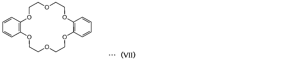
発光装置用封止剤には、シランカップリング剤が含まれていてもよい。シランカップリング剤が加水分解されて発現する水酸基は、発光素子表面に存在する水酸基と脱水縮合反応してシロキサン結合する。また、当該水酸基はポリシロキサン(第一のポリシロキサン及び第二のポリシロキサン)とも反応して、シロキサン結合を形成する。したがって、発光装置用封止剤にシランカップリング剤が含まれると、発光装置用封止剤の硬化物と発光素子との密着性がさらに高まる結果、水蒸気等と発光装置の接触が抑制されるために湿熱耐性が向上する。
[化3]

蛍光体含有封止剤のpHは、1~4であることが好ましい。pHが1未満もしくは4を超えると、ポリシロキサンもしくは有機金属化合物が反応してしまい、保存時に沈殿等が生じる場合がある。蛍光体含有封止剤のpH調整のため、必要に応じて、例えば硝酸等、pH調整剤等を添加してもよい。
蛍光体含有封止剤は、溶媒に、蛍光体粒子、ポリシロキサン、有機金属化合物、及び必要に応じて、無機微粒子、平板状粒子等を混合して調製する。
蛍光体含有封止剤は、例えば図2の概略断面図に示すような、LED装置100の封止層6を成膜に用いられる。当該LED装置では、封止層6が、LEDチップ3やメタル部2等の封止機能だけでなく、LEDチップ3から出射する光の波長を変換する波長変換機能も担う。当該封止層6は、発光素子のパッケージ1、メタル部2、LEDチップ3を保護するガラス基板5等を被覆するように、蛍光体含有封止剤を塗布し、これを乾燥・硬化させることで成膜し得る。
本発明の発光装置は、発光素子と、前述の発光素子用封止剤の硬化膜からなる封止層とを有する。発光装置としては、以下の3つの構成を有する発光装置が挙げられるが、本発明はこれに限定されるものではない。
第1の発光装置は、例えば図2Aの概略断面図に示す発光素子と、これを被覆する封止層とを有する。第1の発光装置における発光素子は、パッケージ(LED基板)1と、メタル部(メタル配線)2と、パッケージ1に配置されたLEDチップ3と、メタル部2とLEDチップ3とを接続する突起電極4と、LEDチップ3の発光面を覆うガラス基板5とを有する。このように、突起電極4を介してメタル部2とLEDチップ3とを接続する態様を、フリップチップ型という。
パッケージ1は、例えば液晶ポリマーやセラミックであるが、絶縁性と耐熱性を有していれば、その材質は特に限定されない。またその形状も特に制限はなく、平板状であってもよく、また凹部を有する形状であってもよい。
波長変換型封止層6の厚みは、LED装置が必要とする蛍光体の量に応じて設定されるため、特に限定されない。ただし、波長変換型封止層6の厚みを10μm以上500μm未満とすることが望ましい。これは、波長変換型封止層6の膜厚が10μm未満の場合は、10~20μmの粒径である一般的な蛍光体粒子を保持するのに膜厚が十分でなく、蛍光体粒子のはがれが起こり、色度ばらつきの原因となるためである。また、蛍光体粒子のはがれが封止層のパスとなり、硫化耐性も低下してしまう。また、発光装置用封止材の膜厚が500μm以上の場合には、光源(即ち、LEDチップ3)からの光が波長変換型封止層6中を通過し、出射するまでに当たる蛍光体粒子の数の差が大きくなり、発光装置の中央付近と周辺付近で色度が変わってしまうという問題が起きてしまうためである。
波長変換型封止層6の形成方法は、前述の蛍光体含有封止剤を成膜して形成する方法(1液型)、及び前述のバインダ型封止剤と蛍光体分散液とをそれぞれ成膜して形成する方法(2液型)に大別される。
波長変換型封止層6を1液型で形成する場合には、前述の発光素子上に、前述の蛍光体含有封止剤を塗布し、これを硬化させる方法でありうる。
波長変換型封止層6を2液型で形成する方法は、1)前述の発光素子を被覆するように、蛍光体分散液を塗布して蛍光体粒子を配置する工程と、2)蛍光体分散液を塗布した発光素子を被覆するように、前述のバインダ型封止剤を塗布し、硬化させる工程とを行う方法でありうる。当該方法によれば、内部に蛍光体含有粒子を含む波長変換型封止層6が成膜される。
蛍光体分散液は、蛍光体粒子と、平板状粒子とを溶媒に分散させた分散液等とすることができ、さらに無機微粒子等が含まれてもよい。すなわち、ポリシロキサン、及び有機金属化合物が含まれないこと以外は、蛍光体含有封止剤と同様である。つまり、各成分(蛍光体粒子、平板状粒子、無機微粒子)や溶媒の種類など、前述の蛍光体含有封止剤と同様に調製すればよい。
蛍光体分散液は、前記発光素子の、少なくともメタル部(メタル配線)2と、パッケージ1に配置されたLEDチップ3の側面と、ガラス基板5とを覆うように塗布する。塗布の手段は特に限定されないが、ブレード塗布、スピンコート塗布、ディスペンサー塗布、スプレー塗布などが例示される。特に、スプレー塗布は薄い塗布膜を成膜しやすく、好ましい。蛍光体分散液の塗布後、必要に応じて、塗膜を乾燥させる。
バインダ型封止剤は、前記蛍光体粒子を覆うように塗布する。塗布の手段は特に限定されないが、ブレード塗布、スピンコート塗布、ディスペンサー塗布、スプレー塗布などが例示される。特に、スプレー塗布は薄い塗布膜を成膜しやすいために好ましい。
第2の発光装置は、例えば図2Bの概略断面図に示す発光素子と、これを被覆する封止層とを有する。第2の発光装置における発光素子は、例えばパッケージ(LED基板)1と、メタル部(メタル配線)2と、パッケージ1に配置されたLEDチップ3と、メタル部2とLEDチップ3とを接続する突起電極4とを有する。
第3の発光装置は、例えば図2Cの概略断面図に示す発光素子と、この発光素子を被覆する封止層7と、この封止層7上に形成された、LEDチップ3からの出射光を波長変換するための蛍光体含有樹脂層8を有する。
封止層は、発光素子のパッケージ(LED基板)1と、メタル部(メタル配線)2と、パッケージ1に配置されたLEDチップ3と、LEDチップ3の発光面とを被覆する。
封止層7は、前述のバインダ型封止剤を塗布して、成膜し得る。具体的には、上述したバインダ型封止剤を、発光素子の、メタル部(メタル配線)2と、パッケージ1に配置されたLEDチップ3と、メタル部2とLEDチップ3とを接続する突起電極4と、LEDチップ3の発光面を覆うように塗布する。塗布の手段は特に限定されないが、ブレード塗布、スピンコート塗布、ディスペンサー塗布、スプレー塗布などが例示される。特に、スプレー塗布は薄い塗布膜を成膜しやすいために好ましい。
蛍光体含有樹脂層8は、LEDチップの発光波長を変換するための層であり、前述の封止層7上に積層される。蛍光体含有樹脂層8は、透明樹脂中に蛍光体粒子が分散した層である。蛍光体粒子は、前述の蛍光体含有封止剤に含まれる蛍光体粒子と同様でありうる。また透明樹脂は、例えば透明の熱硬化性樹脂とすることができ、具体的には、シリコーン樹脂、エポキシ樹脂等が挙げられ、特にシリコーン樹脂が好ましい。
前述の発光装置には、さらに他の光学部品(レンズなど)が設けられて各種光学部材とされる。特に、本発明の発光装置は、硫化ガス耐性や、耐光性、耐熱性等に優れることから、車輌用の照明や、屋外で使用する照明用途等に好適である。
各実施例及び各比較例の発光装置用封止材について、以下の条件で固体Si-NMRスペクトル測定及び波形分離解析を行なった。得られた波形データより、各実施例及び各比較例の発光装置用封止材について、各々のピークの半値幅を求めた。また、全ピーク面積に対するシラノール由来のピーク面積の比率より、全ケイ素原子中のシラノールとなっているケイ素原子の比率(%)を求め、別に分析したケイ素含有率と比較することによりシラノール含有率を求めた。
装置:Chemagnetics社 Infinity CMX-400 核磁気共鳴分光装置
29Si共鳴周波数:79.436MHz
プローブ:7.5mmφCP/MAS用プローブ
測定温度:室温
試料回転数:4kHz
測定法:シングルパルス法
1Hデカップリング周波数:50kHz
29Siフリップ角:90゜
29Si90゜パルス幅:5.0μs
くり返し時間:600s
積算回数:128回
観測幅:30kHz
ブロードニングファクター:20Hz
実施例1~24及び比較例1~9の発光装置用封止材については、512ポイントを測定データとして取り込み、8192ポイントにゼロフィリングしてフーリエ変換した。
フーリエ変換後のスペクトルの各ピークについてローレンツ波形及びガウス波形或いは両者の混合により作成したピーク形状の中心位置、高さ、半値幅を可変パラメータとして、非線形最小二乗法により最適化計算を行なった。
作製したLED装置を、ヒートショック試験機(エスペック社製)を用いて、-30℃(30分)と100℃(30分)との間でサイクル処理を行う。この処理後に、膜はがれによるLED装置の不点灯が発生するかを調べ、下記の基準で硫化耐性評価を行った。
◎:ヒートショック2000サイクルで不点灯無し
○:ヒートショック1500サイクル以上、2000サイクル未満で不点灯発生
△:ヒートショック1000サイクル以上、1500サイクル未満で不点灯発生
×:ヒートショック1000サイクル未満で不点灯発生
JIS規格のガス暴露試験(JIS C 60068-2-43)にもとづき、LEDチップを硫化水素ガス15ppm、温度25℃、相対湿度75%RHの環境下、1000時間暴露する前後で全光束測定を行い、下記の基準で硫化耐性評価を行った。
◎:全光束対初期比(未処理品全光束値/硫化ガス処理後全光束値 ×100)が98%以上である
○:全光束対初期比(未処理品全光束値/硫化ガス処理後全光束値 ×100)が96%以上である
△:全光束対初期比(未処理品全光束値/硫化ガス処理後全光束値 ×100)が92%以上96%未満である
×:全光束対初期比(未処理品全光束値/硫化ガス処理後全光束値 ×100)が92%以下である
SEM(VE7800, Keyence社製)により拡大倍率1000倍でLEDチップの外観観察を行い、下記の基準でクラック耐性評価を行った。
◎:塗膜に5μm以上の長さの亀裂が無い
○:塗膜に10μm以上の長さの亀裂が無い
△:塗膜に10μm以上の長さの亀裂が1本以上5本以下有る
×:塗膜に10μm以上の長さの亀裂が5本以上有る
湿熱試験機SH251(エスペック社製)を用いて、LEDチップを80℃、90%Rhの環境下、1000時間暴露する前後で全光束測定を行い、下記の基準で湿熱耐性評価を行った。
◎:全光束対初期比(未処理品全光束値/湿熱処理後全光束値 ×100)が98%以上である
○:全光束対初期比(未処理品全光束値/湿熱処理後全光束値 ×100)が96%以上である
△:全光束対初期比(未処理品全光束値/湿熱処理後全光束値 ×100)が92%以上96%未満である
×:全光束対初期比(未処理品全光束値/ 湿熱処理後全光束値 ×100)が92%以下である
作製したLED装置の光取り出し性を、分光放射輝度計(CS-1000;コニカミノルタセンシング社製)を用いて測定した。測定条件としては10mAの電流を印加し、封止層を有さないLED装置の全光束値を1.0とした時の相対値により下記の基準で評価した。
◎:相対値が1.1以上である
○:相対値が1.03~1.09である
△:相対値が0.98~1.02である
×:相対値が0.97以下である
実施例5、実施例12及び実施例13で用いた発光装置用封止剤をスライドガラス上に塗布し、実施例5、実施例12及び実施例13に記載の温度で焼成した。この際、焼成後の膜厚が10μm厚となるように積層した。当該スライドガラスについて、メタルハライドランプ耐光性試験機(M6T,スガ試験機社製)で150mW、100時間処理する前後の透過率を測定し、下記の基準で耐光性を評価した。
○:処理後に波長300nm~500nmの光の平均透過率が1.0%未満低下
△:処理後に波長300nm~500nmの光の平均透過率低下が1.0%以上1.5%未満
×:処理後に波長300nm~500nmの光の平均透過率低下が1.5%以上
各実施例及び比較例のLED装置について、(i)LED装置正面における出射光の色度、(ii)LED装置正面から60°傾けた場合の出射光の色度、(iii)LED装置正面から-60°((ii)とは反対方向に60°)傾けた場合の出射光の色度を測定した。色度は分光放射輝度計(CS-1000A、コニカミノルタセンシング社製)で、CIE表色系のx値とy値を測定した。x+y+z=1の関係から得られるz座標は省略した。測定された各色度(x値及びy値)について、それぞれ標準偏差を求めた。そして、x値の標準偏差及びy値の標準偏差の平均値で評価した。評価基準を下記に示す。
○:標準偏差の平均値が0.01以下である
△:標準偏差の平均値が0.01より大きく、0.02以下である
×:標準偏差の平均値が0.02より大きい
蛍光体原料として、Y2O37.41g、Gd2O34.01g、CeO20.63g、及びAl2O37.77gを十分に混合した。これにフラックスとしてフッ化アンモニウムを適量混合し、アルミ製の坩堝に充填した。当該充填物を、水素含有窒素ガスを流通させた還元雰囲気中において、1350~1450℃の温度範囲で2~5時間焼成して焼成品((Y0.72Gd0.24)3Al5O12:Ce0.04)を得た。
実施例1として、サンプルであるLED装置1-1の具体的な作製条件と、その評価結果について説明する。まず、メチルトリメトキシシラン23.6g、テトラメトキシシラン39.3g、メタノール40.0g、及びアセトン40.0gを混合して、これを撹拌した。そこに、水54.6g及び60%硝酸4.7μLを加え、さらに3時間撹拌した。その後、26℃で2日間熟成させた。得られた組成物をポリシロキサン固形分値が10%となるようにメタノールで希釈し、3官能モノメチルシラン化合物:4官能シラン化合物の重合モル比が4:6である発光装置用封止剤を得た。
次に、実施例2として、サンプルであるLED装置1-2の具体的な作製条件と、その評価結果について説明する。本実施例では、発光装置用封止剤を調製する際のシラン化合物を、メチルトリメトキシシランの添加量を29.5g、テトラメトキシシランの添加量を32.8gとし、3官能モノメチルシラン化合物:4官能シラン化合物の重合モル比を4:6とした。なお、その他の条件については、LED装置1-1と同様である。このようにして、LED装置1-2を得た。
次に、実施例3として、サンプルであるLED装置1-3の具体的な作製条件と、その評価結果について説明する。本実施例では、発光装置用封止剤を調製する際のシラン化合物を、メチルトリメトキシシランの添加量を35.4g、テトラメトキシシランの添加量を26.2gとし、3官能モノメチルシラン化合物:4官能シラン化合物の重合モル比を6:4とした。なお、その他の条件については、LED装置1-1と同様である。このようにして、LED装置1-3を得た。
次に、実施例4として、サンプルであるLED装置1-4の具体的な作製条件と、その評価結果について説明する。本実施例では、発光装置用封止剤を調製する際のシラン化合物を、ジメトキシジメチルシランの添加量を13.0g、メチルトリメトキシシランの添加量を29.4g、テトラメトキシシランの添加量を16.4gとし、2官能ジノメチルシラン化合物:3官能モノメチルシラン化合物:4官能シラン化合物の重合モル比を25:50:25とした。なお、その他の条件については、LED装置1-1と同様である。このようにして、LED装置1-4を得た。
次に、実施例5として、サンプルであるLED装置1-5の具体的な作製条件と、その評価結果について説明する。本実施例では、発光装置用封止剤を調製する際のシラン化合物を、ジメトキシジメチルシランの添加量を6.0g、メチルトリメトキシシランの添加量を23.4g、テトラメトキシシランの添加量を29.5gとし、2官能ジノメチルシラン化合物:3官能モノメチルシラン化合物:4官能シラン化合物の重合モル比を15:40:45とし、固形分濃度10%の発光装置用封止剤を得た。なお、その他の条件については、LED装置1-1と同様である。このようにして、LED装置1-5を得た。
次に、実施例6として、サンプルであるLED装置1-6の具体的な作製条件と、その評価結果について説明する。本実施例では、発光装置用封止剤を調製する際のシラン化合物を、ジメトキシジメチルシランの添加量を5.2g、メチルトリメトキシシランの添加量を17.6g、テトラメトキシシランの添加量を39.4gとし、2官能ジノメチルシラン化合物:3官能モノメチルシラン化合物:4官能シラン化合物の重合モル比を10:30:60とした。なお、その他の条件については、LED装置1-1と同様である。このようにして、LED装置1-6を得た。
次に、実施例7として、サンプルであるLED装置1-7の具体的な作製条件と、その評価結果について説明する。本実施例では、発光装置用封止剤を調製する際のシラン化合物を、ジメトキシジメチルシランの添加量を13.0g、メチルトリメトキシシランの添加量を29.3g、テトラメトキシシランの添加量を16.4gとし、2官能ジノメチルシラン化合物:3官能モノメチルシラン化合物:4官能シラン化合物の重合モル比を25:50:25とした。なお、その他の条件については、LED装置1-1と同様である。このようにして、LED装置1-7を得た。
次に、実施例8として、サンプルであるLED装置1-8の具体的な作製条件と、その評価結果について説明する。本実施例では、発光装置用封止剤を調製する際のシラン化合物を、ジメトキシジメチルシランの添加量を5.2g、メチルトリメトキシシランの添加量を17.6g、テトラメトキシシランの添加量を39.4gとし、2官能ジノメチルシラン化合物:3官能モノメチルシラン化合物:4官能シラン化合物の重合モル比を10:30:60とした。なお、その他の条件については、LED装置1-1と同様である。このようにして、LED装置1-8を得た。
次に、比較例1として、サンプルであるLED装置1-9の具体的な作製条件と、その評価結果について説明する。この比較例では、発光装置用封止剤を調製する際のシラン化合物を、テトラメトキシシラン65.6gとし、2官能ジノメチルシラン化合物:3官能モノメチルシラン化合物:4官能シラン化合物の重合モル比を0:0:100とした。なお、その他の条件については、LED装置1-1と同様である。このようにして、LED装置1-9を得た。
次に、比較例2として、サンプルであるLED装置1-10の具体的な作製条件と、その評価結果について説明する。この比較例では、発光装置用封止剤を調製する際のシラン化合物を、メチルトリメトキシシラン58.7gとし、2官能ジノメチルシラン化合物:3官能モノメチルシラン化合物:4官能シラン化合物の重合モル比を0:100:0とした。なお、その他の条件については、LED装置1-1と同様である。このようにして、LED装置1-10を得た。
次に、比較例3として、サンプルであるLED装置1-11の具体的な作製条件と、その評価結果について説明する。この比較例では、発光装置用封止剤を調製する際のシラン化合物を、ジメトキシジメチルシラン51.8gとし、2官能ジノメチルシラン化合物:3官能モノメチルシラン化合物:4官能シラン化合物の重合モル比を100:0:0とした。なお、その他の条件については、LED装置1-1と同様である。このようにして、LED装置1-11を得た。
次に、比較例4として、サンプルであるLED装置1-12の具体的な作製条件と、その評価結果について説明する。この比較例では、発光装置用封止剤を調製する際のシラン化合物を、ジメトキシジメチルシラン20.8g、メチルトリメトキシシランの添加量を35.3gとし、2官能ジノメチルシラン化合物:3官能モノメチルシラン化合物:4官能シラン化合物の重合モル比を40:60:0とした。なお、その他の条件については、LED装置1-1と同様である。このようにして、LED装置1-12を得た。
次に、比較例5として、サンプルであるLED装置1-13の具体的な作製条件と、その評価結果について説明する。この比較例では、発光装置用封止剤を調製する際のシラン化合物を、ジメトキシジメチルシラン26.0g、テトラメトキシシランの添加量を32.9gとし、2官能ジノメチルシラン化合物:3官能モノメチルシラン化合物:4官能シラン化合物の重合モル比を50:0:50とした。なお、その他の条件については、LED装置1-1と同様である。このようにして、LED装置1-13を得た。
次に、比較例6として、サンプルであるLED装置1-14の具体的な作製条件と、その評価結果について説明する。この比較例では、発光装置用封止剤を調製する際のシラン化合物を、メチルトリメトキシシランの添加量を44.1g、テトラメトキシシランの添加量を5.5gとし、2官能ジノメチルシラン化合物:3官能モノメチルシラン化合物:4官能シラン化合物の重合モル比を0:90:10とした。なお、その他の条件については、LED装置1-1と同様である。このようにして、LED装置1-14を得た。
次に、比較例7として、サンプルであるLED装置1-15の具体的な作製条件と、その評価結果について説明する。この比較例では、発光装置用封止剤を調製する際のシラン化合物を、メチルトリメトキシシランの添加量を4.9g、テトラメトキシシランの添加量を49.3gとし、2官能ジノメチルシラン化合物:3官能モノメチルシラン化合物:4官能シラン化合物の重合モル比を0:10:90とした。なお、その他の条件については、LED装置1-1と同様である。このようにして、LED装置1-15を得た。
次に、比較例8として、サンプルであるLED装置1-16の具体的な作製条件と、その評価結果について説明する。この比較例では、発光装置用封止剤を調製する際のシラン化合物を、ジメトキシジメチルシラン30.3g、メチルトリメトキシシランの添加量を9.8g、テトラメトキシシランの添加量を5.5gとし、2官能ジノメチルシラン化合物:3官能モノメチルシラン化合物:4官能シラン化合物の重合モル比を70:20:10とした。なお、その他の条件については、LED装置1-1と同様である。このようにして、LED装置1-16を得た。
次に、比較例9として、サンプルであるLED装置1-17の具体的な作製条件と、その評価結果について説明する。この比較例では、発光装置用封止剤を調製する際のシラン化合物を、ジメトキシジメチルシラン4.3g、メチルトリメトキシシランの添加量を14.7g、テトラメトキシシランの添加量を32.9gとし、2官能ジノメチルシラン化合物:3官能モノメチルシラン化合物:4官能シラン化合物の重合モル比を10:30:60とした。なお、その他の条件については、LED装置1-1と同様である。このようにして、LED装置1-17を得た。
・固体Si-NMRスペクトルにおいて、ピークトップの位置がケミカルシフト-120ppm以上-90ppm以下の領域に存在し(即ち、Qnピーク群)、半値幅が5ppm以上12ppm以下であるピークを有する。かつ
・固体Si-NMRスペクトルにおいて、ピークトップの位置がケミカルシフト-80ppm以上-40ppm以下の領域に存在し(即ち、Tnピーク群)、半値幅が5ppm以上12ppm以下であるピークを有する。かつ
・シラノール含有率が11重量%以上30重量%以下である。
実施例9として、サンプルであるLED装置1-18の具体的な作製条件と、その評価結果について説明する。本実施例では、発光装置用封止剤を調製する際に、LED装置1-5作製で用いた発光装置用封止剤に、さらにZrO2微粒子が分散したスラリー(TECNADIS-ZR-220、TECNAN社製)をZrO2微粒子が固形分全体の15%となるように添加した。なお、その他の条件については、LED装置1-5と同様である。このようにして、LED装置1-18を得た。
次に、実施例10として、サンプルであるLED装置1-19の具体的な作製条件と、その評価結果について説明する。本実施例では、発光装置用封止剤を調製する際に、LED装置1-5作製で用いた発光装置用封止剤に、さらにTiO2微粒子が分散したスラリー(TECNADIS-TI-220、TECNAN社製)をTiO2微粒子が固形分全体の15重量%となるように添加した。なお、その他の条件については、LED装置1-5と同様である。このようにして、LED装置1-19を得た。
次に、実施例11として、サンプルであるLED装置1-20の具体的な作製条件と、その評価結果について説明する。本実施例では、発光装置用封止剤を調製する際に、LED装置1-5作製で用いた発光装置用封止剤に、さらにAl2O3微粒子が分散したスラリー(TECNADIS-AL-220、TECNAN社製)をAl2O3微粒子が固形分全体の15%となるように添加した。なお、その他の条件については、LED装置1-5と同様である。このようにして、LED装置1-20を得た。
実施例12として、サンプルであるLED装置1-21の具体的な作製条件と、その評価結果について説明する。本実施例では、発光装置用封止剤(バインダ型封止剤)を、蛍光体粒子上にスプレー塗布した後に、80℃で1時間焼成を行っている。なお、その他の条件については、LED装置1-5と同様である。このようにして、LED装置1-21を得た。
次に、実施例13として、サンプルであるLED装置1-22の具体的な作製条件と、その評価結果について説明する。本実施例では発光装置用封止剤(バインダ型封止剤)を、蛍光体粒子上にスプレー塗布した後に、100℃で1時間焼成を行っている。なお、その他の条件については、LED装置1-5と同様である。このようにして、LED装置1-22を得た。
実施例14として、サンプルであるLED装置1-23の具体的な作製条件と、その評価結果について説明する。本実施例では、蛍光体分散液を調整する際に、MK-100(合成雲母、コープケミカル社製)の添加量を0.02gとした。なお、その他の条件については、LED装置1-5と同様である。このようにして、LED装置1-23を得た。この条件で封止層を形成した場合、その膜厚は100μmとなる。
次に、実施例15として、サンプルであるLED装置1-24の具体的な作製条件と、その評価結果について説明する。本実施例では、蛍光体分散液を調整する際に、MK-100(合成雲母、コープケミカル社製)の添加量を0.45gとした。なお、その他の条件については、LED装置1-5と同様である。このようにして、LED装置1-24を得た。この条件で封止層を形成した場合、その膜厚は450μmとなる。
実施例16として、サンプルであるLED装置3-23の具体的な作製条件と、その評価結果について説明する。本実施例では、膜厚が0.7μmとなるように封止層7を形成している。なお、その他の条件については、LED装置3-18と同様である。
次に、実施例17として、サンプルであるLED装置3-24の具体的な作製条件と、その評価結果について説明する。本実施例では、膜厚が1.5μmとなるように封止層7を形成している。なお、その他の条件については、LED装置3-18と同様である。
次に、実施例18として、サンプルであるLED装置3-25の具体的な作製条件と、その評価結果について説明する。本実施例では、膜厚が5μmとなるように封止層7を形成している。なお、その他の条件については、LED装置3-18と同様である。
次に、実施例19として、サンプルであるLED装置3-26の具体的な作製条件と、その評価結果について説明する。本実施例では、膜厚が15μmとなるように封止層7を形成している。なお、その他の条件については、LED装置3-18と同様である。
次に、実施例20として、サンプルであるLED装置3-27の具体的な作製条件と、その評価結果について説明する。本実施例では、発光装置用封止剤を調製する際に、LED装置3-18作製で用いた発光装置用封止剤に、さらにジベンゾ-18-クラウン6-エーテルが固形分全体の2重量%となるように添加した。なお、その他の条件については、LED装置3-18と同様である。
次に、実施例21として、サンプルであるLED装置3-28の具体的な作製条件と、その評価結果について説明する。本実施例では、発光装置用封止剤を調製する際に、LED装置3-18作製で用いた発光装置用封止剤に、さらに3-アミノプロピルトリメトキシシランが固形分全体の1重量%となるように添加した。なお、その他の条件については、LED装置3-18と同様である。
次に、実施例22として、サンプルであるLED装置3-29の具体的な作製条件と、その評価結果について説明する。本実施例では、発光装置用封止剤を調製する際に、LED装置3-18作製で用いた発光装置用封止剤に、さらに3-メルカプトプロピルメチルジメトキシシランが固形分全体の1重量%となるように添加した。なお、その他の条件については、LED装置3-18と同様である。
次に、実施例23として、サンプルであるLED装置3-30の具体的な作製条件と、その評価結果について説明する。本実施例では、発光装置用封止剤を調製する際に、LED装置3-18作製で用いた発光装置用封止剤に、さらにジベンゾ-18-クラウン6-エーテルが固形分全体の1重量%、3-アミノプロピルトリメトキシシランが固形分全体の0.5重量%となるように添加した。なお、その他の条件については、LED装置3-18と同様である。
次に、実施例24として、サンプルであるLED装置3-31の具体的な作製条件と、その評価結果について説明する。本実施例では、発光装置用封止剤を調製する際に、LED装置3-18作製で用いた発光装置用封止剤に、さらにジベンゾ-18-クラウン6-エーテルが固形分全体の1重量%、3-メルカプトプロピルメチルジメトキシシランが固形分全体の0.5重量%となるように添加した。なお、その他の条件については、LED装置3-18と同様である。
・固体Si-NMRスペクトルにおいて、ピークトップの位置がケミカルシフト-120ppm以上-90ppm以下の領域に存在し(即ち、Qnピーク群)、半値幅が5ppm以上12ppm以下であるピークを有する。かつ
・固体Si-NMRスペクトルにおいて、ピークトップの位置がケミカルシフト-80ppm以上-40ppm以下の領域に存在し(即ち、Tnピーク群)、半値幅が5ppm以上12ppm以下であるピークを有する。かつ
・シラノール含有率が11重量%以上30重量%以下である。
これにより、この発光装置用封止材は、密着性とクラック耐性が両立し、かつ、高い硫化耐性と湿熱耐性を得ることが可能となる。
2 メタル部
3 LEDチップ
4 突起電極
5 ガラス基板
6 波長変換型封止層
7 封止層
8 蛍光体含有樹脂層
100 LED装置
Claims (10)
- 発光素子を封止するための発光装置用封止材であって、
固体Si-核磁気共鳴スペクトルにおいて、ピークトップの位置がケミカルシフト-120ppm以上-90ppm以下の領域に存在し、半値幅が5ppm以上12ppm以下であるピークと、
固体Si-核磁気共鳴スペクトルにおいて、ピークトップの位置がケミカルシフト-80ppm以上-40ppm以下の領域に存在し、半値幅が5ppm以上12ppm以下であるピークとを有し、かつ、
シラノール含有率が11重量%以上30重量%以下であることを特徴とする発光装置用封止材。 - 無機酸化微粒子を含有することを特徴とする請求項1に記載の発光装置用封止材。
- 前記無機酸化微粒子は、ZrO2であることを特徴とする請求項2に記載の発光装置用封止材。
- 環状エーテル化合物を含有することを特徴とする請求項1に記載の発光装置用封止材。
- シランカップリング剤を含有することを特徴とする請求項1に記載の発光装置用封止材。
- 蛍光体粒子を含有することを特徴とする請求項1~請求項5のいずれか一つに記載の発光装置用封止材。
- 発光素子の少なくとも発光面が封止層で覆われた発光装置であって、
前記封止層は、請求項1~請求項6のいずれか一つに記載の発光装置用封止材により形成され、その膜厚が10μm以上500μm未満であることを特徴とする発光装置。 - 発光素子の少なくとも発光面が封止層で覆われ、前記封止層上に、樹脂及び蛍光体粒子を含む蛍光体含有樹脂層を有する発光装置であって、
前記封止層は、請求項1~請求項5のいずれか一つに記載の発光装置用封止材により形成され、膜厚が0.7μm以上15μm以下であることを特徴とする発光装置。 - 前記発光素子が、発光ダイオードであることを特徴とする請求項7または請求項8に記載の発光装置。
- 発光素子の少なくとも発光面が封止層で覆われた発光装置の製造方法であって、
前記発光素子上に、発光装置用封止剤を塗布する工程と、
前記発光装置用封止剤を80℃以上で硬化させることで、請求項1~請求項6のいずれか一つに記載の発光装置用封止材を含む封止層を形成する工程と、
を備えたことを特徴とする発光装置の製造方法。
Priority Applications (3)
| Application Number | Priority Date | Filing Date | Title |
|---|---|---|---|
| EP13796330.2A EP2865703A4 (en) | 2012-05-31 | 2013-05-31 | SEALANT FOR LIGHT-EMITTING DEVICE, LIGHT-EMITTING DEVICE THEREWITH AND LIGHT-EMITTING DEVICE MANUFACTURING METHOD |
| US14/404,183 US9269874B2 (en) | 2012-05-31 | 2013-05-31 | Sealing material for light emitting device, light emitting device using the same, and manufacturing method for light emitting device |
| JP2014518749A JPWO2013180259A1 (ja) | 2012-05-31 | 2013-05-31 | 発光装置用封止材、及びこれを用いた発光装置、並びに発光装置の製造方法 |
Applications Claiming Priority (2)
| Application Number | Priority Date | Filing Date | Title |
|---|---|---|---|
| JP2012124166 | 2012-05-31 | ||
| JP2012-124166 | 2012-05-31 |
Publications (1)
| Publication Number | Publication Date |
|---|---|
| WO2013180259A1 true WO2013180259A1 (ja) | 2013-12-05 |
Family
ID=49673442
Family Applications (1)
| Application Number | Title | Priority Date | Filing Date |
|---|---|---|---|
| PCT/JP2013/065151 Ceased WO2013180259A1 (ja) | 2012-05-31 | 2013-05-31 | 発光装置用封止材、及びこれを用いた発光装置、並びに発光装置の製造方法 |
Country Status (4)
| Country | Link |
|---|---|
| US (1) | US9269874B2 (ja) |
| EP (1) | EP2865703A4 (ja) |
| JP (1) | JPWO2013180259A1 (ja) |
| WO (1) | WO2013180259A1 (ja) |
Cited By (5)
| Publication number | Priority date | Publication date | Assignee | Title |
|---|---|---|---|---|
| US20160266111A1 (en) * | 2013-10-31 | 2016-09-15 | Konica Minolta, Inc. | Detection Device, Detection Method Using Said Detection Device, And Detection Chip Used In Said Detection Device |
| CN106661425A (zh) * | 2014-07-28 | 2017-05-10 | 住友化学株式会社 | 硅酮系密封材料组合物及半导体发光装置 |
| JP2019169707A (ja) * | 2018-03-20 | 2019-10-03 | オスラム オプト セミコンダクターズ ゲゼルシャフト ミット ベシュレンクテル ハフツングOsram Opto Semiconductors GmbH | オプトエレクトロニクス部品 |
| JP2021533576A (ja) * | 2018-08-17 | 2021-12-02 | オスラム オプト セミコンダクターズ ゲゼルシャフト ミット ベシュレンクテル ハフツングOsram Opto Semiconductors GmbH | 光電子部品及び光電子部品を製造するための方法 |
| JP2022532182A (ja) * | 2019-05-10 | 2022-07-13 | オスラム オプト セミコンダクターズ ゲゼルシャフト ミット ベシュレンクテル ハフツング | 光電素子および光電素子の製造方法 |
Families Citing this family (7)
| Publication number | Priority date | Publication date | Assignee | Title |
|---|---|---|---|---|
| IT201700056441A1 (it) * | 2017-05-24 | 2018-11-24 | Automotive Lighting Italia Spa | Dispositivo di illuminazione per veicoli con coperchio di montaggio lampada perfezionato |
| WO2019056209A1 (en) * | 2017-09-20 | 2019-03-28 | Materion Precision Optics (Shanghai) Limited | LUMINOPHORE WHEEL WITH INORGANIC BINDER |
| DE102018110187A1 (de) * | 2018-04-27 | 2019-10-31 | Osram Opto Semiconductors Gmbh | Optoelektronischer Halbleiterkörper, Anordnung von einer Vielzahl von optoelektronischen Halbleiterkörpern und Verfahren zur Herstellung eines optoelektronischen Halbleiterkörpers |
| CN112898780A (zh) * | 2019-12-04 | 2021-06-04 | 明基材料股份有限公司 | 具阻水气特性的硅胶薄膜 |
| US11584882B2 (en) * | 2020-02-14 | 2023-02-21 | Osram Opto Semiconductors Gmbh | Wavelength converter; method of its making and light-emitting device incorporating the element |
| TW202221082A (zh) * | 2020-11-17 | 2022-06-01 | 明基材料股份有限公司 | 一種矽膠阻氣膜 |
| US12256629B2 (en) * | 2021-11-19 | 2025-03-18 | Osram Opto Semiconductors Gmbh | Curable self-adhesive wavelength converting film and light emitting device comprising the same |
Citations (8)
| Publication number | Priority date | Publication date | Assignee | Title |
|---|---|---|---|---|
| JPH0971654A (ja) * | 1995-07-05 | 1997-03-18 | Shin Etsu Chem Co Ltd | オルガノポリシロキサン樹脂及びその製造方法並びにそれを用いた硬化性オルガノポリシロキサン樹脂組成物 |
| JP2003292626A (ja) * | 2002-03-29 | 2003-10-15 | Jsr Corp | 絶縁膜形成用塗布液 |
| JP2005309215A (ja) * | 2004-04-23 | 2005-11-04 | Hitachi Chemical Dupont Microsystems Ltd | 感光性重合体組成物及びそれを用いたレリ−フパターンの製造法、電子部品。 |
| JP2006229221A (ja) * | 1994-03-11 | 2006-08-31 | Kawasaki Microelectronics Kk | 絶縁膜形成用塗布液および半導体装置用絶縁膜の形成方法 |
| JP2007112975A (ja) | 2005-02-23 | 2007-05-10 | Mitsubishi Chemicals Corp | 半導体発光デバイス用部材及びその製造方法、並びにそれを用いた半導体発光デバイス |
| JP2007112974A (ja) | 2005-09-22 | 2007-05-10 | Mitsubishi Chemicals Corp | 半導体発光デバイス用部材及びその製造方法、並びにそれを用いた半導体発光デバイス |
| JP2011026570A (ja) * | 2009-06-24 | 2011-02-10 | Asahi Kasei E-Materials Corp | ポリシロキサン縮合反応物 |
| JP2011159912A (ja) * | 2010-02-03 | 2011-08-18 | Sekisui Chem Co Ltd | 光半導体素子用封止剤及び光半導体装置 |
Family Cites Families (9)
| Publication number | Priority date | Publication date | Assignee | Title |
|---|---|---|---|---|
| JP3078326B2 (ja) | 1994-03-11 | 2000-08-21 | 川崎製鉄株式会社 | 絶縁膜形成用塗布液およびその製造方法ならびに半導体装置用絶縁膜の形成方法およびこれを適用する半導体装置の製造方法 |
| US5844060A (en) | 1995-07-05 | 1998-12-01 | Shin-Etsu Chemical Co., Ltd. | Organopolysiloxane resin, production method thereof, and curable organopolysiloxane resin composition using the same |
| TWI382077B (zh) | 2005-02-23 | 2013-01-11 | 三菱化學股份有限公司 | 半導體發光裝置用構件及其製造方法,暨使用其之半導體發光裝置 |
| US20080012074A1 (en) | 2006-07-14 | 2008-01-17 | Air Products And Chemicals, Inc. | Low Temperature Sol-Gel Silicates As Dielectrics or Planarization Layers For Thin Film Transistors |
| EP2065931A4 (en) * | 2006-08-22 | 2013-02-27 | Mitsubishi Chem Corp | SEMICONDUCTOR ELEMENT ELEMENT, LIQUID TO FORM A SEMICONDUCTOR COMPONENT member, PROCESS FOR PRODUCING A SEMICONDUCTOR COMPONENT link and FLUID TO FORM A SEMICONDUCTOR COMPONENT member USING THE METHOD, FLUORESCENT COMPOSITION, SEMICONDUCTOR LIGHT ELEMENT, ILLUMINATION DEVICE AND IMAGE DISPLAY DEVICE |
| JP2009002767A (ja) | 2007-06-21 | 2009-01-08 | Casio Comput Co Ltd | ガラス取付構造 |
| JP2009276742A (ja) * | 2008-04-18 | 2009-11-26 | Hitachi Chem Co Ltd | 感光性樹脂膜の形成方法、シリカ系被膜の形成方法並びにシリカ系被膜を備える装置及び部材 |
| WO2010150861A1 (ja) | 2009-06-24 | 2010-12-29 | 旭化成イーマテリアルズ株式会社 | ポリシロキサン縮合反応物 |
| US20150221837A1 (en) | 2011-12-26 | 2015-08-06 | Konica Minolta, Inc. | Sealant for led device, led device, and method for producing led device |
-
2013
- 2013-05-31 JP JP2014518749A patent/JPWO2013180259A1/ja active Pending
- 2013-05-31 EP EP13796330.2A patent/EP2865703A4/en not_active Withdrawn
- 2013-05-31 US US14/404,183 patent/US9269874B2/en active Active
- 2013-05-31 WO PCT/JP2013/065151 patent/WO2013180259A1/ja not_active Ceased
Patent Citations (8)
| Publication number | Priority date | Publication date | Assignee | Title |
|---|---|---|---|---|
| JP2006229221A (ja) * | 1994-03-11 | 2006-08-31 | Kawasaki Microelectronics Kk | 絶縁膜形成用塗布液および半導体装置用絶縁膜の形成方法 |
| JPH0971654A (ja) * | 1995-07-05 | 1997-03-18 | Shin Etsu Chem Co Ltd | オルガノポリシロキサン樹脂及びその製造方法並びにそれを用いた硬化性オルガノポリシロキサン樹脂組成物 |
| JP2003292626A (ja) * | 2002-03-29 | 2003-10-15 | Jsr Corp | 絶縁膜形成用塗布液 |
| JP2005309215A (ja) * | 2004-04-23 | 2005-11-04 | Hitachi Chemical Dupont Microsystems Ltd | 感光性重合体組成物及びそれを用いたレリ−フパターンの製造法、電子部品。 |
| JP2007112975A (ja) | 2005-02-23 | 2007-05-10 | Mitsubishi Chemicals Corp | 半導体発光デバイス用部材及びその製造方法、並びにそれを用いた半導体発光デバイス |
| JP2007112974A (ja) | 2005-09-22 | 2007-05-10 | Mitsubishi Chemicals Corp | 半導体発光デバイス用部材及びその製造方法、並びにそれを用いた半導体発光デバイス |
| JP2011026570A (ja) * | 2009-06-24 | 2011-02-10 | Asahi Kasei E-Materials Corp | ポリシロキサン縮合反応物 |
| JP2011159912A (ja) * | 2010-02-03 | 2011-08-18 | Sekisui Chem Co Ltd | 光半導体素子用封止剤及び光半導体装置 |
Non-Patent Citations (1)
| Title |
|---|
| See also references of EP2865703A4 |
Cited By (7)
| Publication number | Priority date | Publication date | Assignee | Title |
|---|---|---|---|---|
| US20160266111A1 (en) * | 2013-10-31 | 2016-09-15 | Konica Minolta, Inc. | Detection Device, Detection Method Using Said Detection Device, And Detection Chip Used In Said Detection Device |
| US11215613B2 (en) * | 2013-10-31 | 2022-01-04 | Konica Minolta, Inc. | Detection device, detection method using said detection device, and detection chip used in said detection device |
| CN106661425A (zh) * | 2014-07-28 | 2017-05-10 | 住友化学株式会社 | 硅酮系密封材料组合物及半导体发光装置 |
| CN106661425B (zh) * | 2014-07-28 | 2018-12-21 | 住友化学株式会社 | 硅酮系密封材料组合物及半导体发光装置 |
| JP2019169707A (ja) * | 2018-03-20 | 2019-10-03 | オスラム オプト セミコンダクターズ ゲゼルシャフト ミット ベシュレンクテル ハフツングOsram Opto Semiconductors GmbH | オプトエレクトロニクス部品 |
| JP2021533576A (ja) * | 2018-08-17 | 2021-12-02 | オスラム オプト セミコンダクターズ ゲゼルシャフト ミット ベシュレンクテル ハフツングOsram Opto Semiconductors GmbH | 光電子部品及び光電子部品を製造するための方法 |
| JP2022532182A (ja) * | 2019-05-10 | 2022-07-13 | オスラム オプト セミコンダクターズ ゲゼルシャフト ミット ベシュレンクテル ハフツング | 光電素子および光電素子の製造方法 |
Also Published As
| Publication number | Publication date |
|---|---|
| EP2865703A4 (en) | 2015-11-18 |
| JPWO2013180259A1 (ja) | 2016-01-21 |
| EP2865703A1 (en) | 2015-04-29 |
| US20150188007A1 (en) | 2015-07-02 |
| US9269874B2 (en) | 2016-02-23 |
Similar Documents
| Publication | Publication Date | Title |
|---|---|---|
| WO2013180259A1 (ja) | 発光装置用封止材、及びこれを用いた発光装置、並びに発光装置の製造方法 | |
| US9708492B2 (en) | LED device and coating liquid used for production of same | |
| WO2013099193A1 (ja) | Led装置用封止剤、led装置、及びled装置の製造方法 | |
| JP2014122296A (ja) | 発光装置用封止材前駆体溶液、これを用いた発光装置用封止材、led装置、並びにled装置の製造方法 | |
| JP2014158011A (ja) | Led装置の製造方法 | |
| JP5843016B2 (ja) | Led装置及びその製造方法 | |
| WO2014103326A1 (ja) | 塗布液、及びその硬化物からなる反射層を備えるled装置 | |
| JPWO2014104295A1 (ja) | 発光装置 | |
| JP2014022508A (ja) | Led装置及びその製造方法 | |
| JP5910340B2 (ja) | Led装置、及びその製造方法 | |
| JP2014130871A (ja) | 発光装置 | |
| WO2013180258A1 (ja) | 発光装置用封止材、及びこれを用いた発光装置、並びに発光装置の製造方法 | |
| JP2014127495A (ja) | Led装置、及びその製造方法 | |
| WO2014103330A1 (ja) | 蛍光体分散液、led装置およびその製造方法 | |
| JP2016154179A (ja) | 発光装置、及びその製造方法 | |
| JP2014130903A (ja) | 半導体発光装置及びその製造方法 | |
| WO2014091762A1 (ja) | Led装置用封止剤、及びこれを用いたled装置 | |
| JP2014041955A (ja) | Led装置、及びその製造方法 | |
| JP5729327B2 (ja) | Led装置の製造方法 | |
| JP2016181535A (ja) | 発光装置、および発光装置製造用の塗布液 | |
| JP2014160713A (ja) | Led装置の製造方法 | |
| WO2016024604A1 (ja) | 無機微粒子含有ポリシルセスキオキサン組成物およびその製造方法、ならびに発光装置およびその製造方法 | |
| WO2015011929A1 (ja) | 発光装置 | |
| WO2015025526A1 (ja) | Led装置及びその製造方法 | |
| JP2016001657A (ja) | ハードコート剤、封止用組成物、積層体、及び発光装置 |
Legal Events
| Date | Code | Title | Description |
|---|---|---|---|
| 121 | Ep: the epo has been informed by wipo that ep was designated in this application |
Ref document number: 13796330 Country of ref document: EP Kind code of ref document: A1 |
|
| ENP | Entry into the national phase |
Ref document number: 2014518749 Country of ref document: JP Kind code of ref document: A |
|
| WWE | Wipo information: entry into national phase |
Ref document number: 14404183 Country of ref document: US |
|
| REEP | Request for entry into the european phase |
Ref document number: 2013796330 Country of ref document: EP |
|
| WWE | Wipo information: entry into national phase |
Ref document number: 2013796330 Country of ref document: EP |
|
| NENP | Non-entry into the national phase |
Ref country code: DE |