WO2013183146A1 - Procédé de détermination d'état de connexion de fibre optique, module optique de détermination d'état de connexion de fibre optique et dispositif d'émission optique - Google Patents
Procédé de détermination d'état de connexion de fibre optique, module optique de détermination d'état de connexion de fibre optique et dispositif d'émission optique Download PDFInfo
- Publication number
- WO2013183146A1 WO2013183146A1 PCT/JP2012/064692 JP2012064692W WO2013183146A1 WO 2013183146 A1 WO2013183146 A1 WO 2013183146A1 JP 2012064692 W JP2012064692 W JP 2012064692W WO 2013183146 A1 WO2013183146 A1 WO 2013183146A1
- Authority
- WO
- WIPO (PCT)
- Prior art keywords
- optical
- optical fiber
- test signal
- connection state
- signal
- Prior art date
- Legal status (The legal status is an assumption and is not a legal conclusion. Google has not performed a legal analysis and makes no representation as to the accuracy of the status listed.)
- Ceased
Links
Images







Classifications
-
- H—ELECTRICITY
- H04—ELECTRIC COMMUNICATION TECHNIQUE
- H04B—TRANSMISSION
- H04B10/00—Transmission systems employing electromagnetic waves other than radio-waves, e.g. infrared, visible or ultraviolet light, or employing corpuscular radiation, e.g. quantum communication
- H04B10/07—Arrangements for monitoring or testing transmission systems; Arrangements for fault measurement of transmission systems
- H04B10/075—Arrangements for monitoring or testing transmission systems; Arrangements for fault measurement of transmission systems using an in-service signal
- H04B10/077—Arrangements for monitoring or testing transmission systems; Arrangements for fault measurement of transmission systems using an in-service signal using a supervisory or additional signal
- H04B10/0775—Performance monitoring and measurement of transmission parameters
-
- G—PHYSICS
- G01—MEASURING; TESTING
- G01M—TESTING STATIC OR DYNAMIC BALANCE OF MACHINES OR STRUCTURES; TESTING OF STRUCTURES OR APPARATUS, NOT OTHERWISE PROVIDED FOR
- G01M11/00—Testing of optical apparatus; Testing structures by optical methods not otherwise provided for
- G01M11/30—Testing of optical devices, constituted by fibre optics or optical waveguides
- G01M11/33—Testing of optical devices, constituted by fibre optics or optical waveguides with a light emitter being disposed at one fibre or waveguide end-face, and a light receiver at the other end-face
- G01M11/335—Testing of optical devices, constituted by fibre optics or optical waveguides with a light emitter being disposed at one fibre or waveguide end-face, and a light receiver at the other end-face using two or more input wavelengths
-
- H—ELECTRICITY
- H04—ELECTRIC COMMUNICATION TECHNIQUE
- H04B—TRANSMISSION
- H04B10/00—Transmission systems employing electromagnetic waves other than radio-waves, e.g. infrared, visible or ultraviolet light, or employing corpuscular radiation, e.g. quantum communication
- H04B10/07—Arrangements for monitoring or testing transmission systems; Arrangements for fault measurement of transmission systems
- H04B10/075—Arrangements for monitoring or testing transmission systems; Arrangements for fault measurement of transmission systems using an in-service signal
- H04B10/077—Arrangements for monitoring or testing transmission systems; Arrangements for fault measurement of transmission systems using an in-service signal using a supervisory or additional signal
- H04B10/0771—Fault location on the transmission path
-
- H—ELECTRICITY
- H04—ELECTRIC COMMUNICATION TECHNIQUE
- H04J—MULTIPLEX COMMUNICATION
- H04J14/00—Optical multiplex systems
- H04J14/02—Wavelength-division multiplex systems
- H04J14/0201—Add-and-drop multiplexing
- H04J14/0202—Arrangements therefor
-
- H—ELECTRICITY
- H04—ELECTRIC COMMUNICATION TECHNIQUE
- H04B—TRANSMISSION
- H04B2210/00—Indexing scheme relating to optical transmission systems
- H04B2210/07—Monitoring an optical transmission system using a supervisory signal
- H04B2210/078—Monitoring an optical transmission system using a supervisory signal using a separate wavelength
Definitions
- the present invention relates to an optical fiber connection state determination method, an optical fiber connection state determination optical module, and an optical transmission device.
- WDM wavelength division multiplexing
- OADM optical add-drop multiplexer
- the optical add / drop device has a function of inserting an optical signal of a desired wavelength into a WDM optical signal (optical add function) and a function of branching an optical signal of a desired wavelength from the WDM optical signal (optical drop function).
- An optical add / drop device that inserts and / or branches an optical signal having a desired wavelength is sometimes referred to as ROADM (Reconfigurable OADM).
- ROADM Reconfigurable OADM
- the optical add / drop multiplexer has a CDC (Colorless, Directionless, and Contentionless) function so that the wavelength path can be set or changed flexibly.
- Colorless means a configuration or function capable of inputting an arbitrary wavelength to an arbitrary port of the optical add / drop multiplexer and outputting an arbitrary wavelength from the arbitrary port.
- Directionless is a configuration in which the optical add / drop multiplexer has a plurality of routes, and can guide the optical signal from each terminal station to an arbitrary route. The optical signal from each route can be transmitted to any terminal station.
- Means a configuration or function that can lead to Further, Contentionless means a configuration or function that avoids collision of optical signals of the same wavelength in the optical add / drop multiplexer.
- Patent Document 1 describes an example of an optical add / drop multiplexer having a CDC function.
- An optical transmission apparatus including such an optical add / drop apparatus has a large number of optical devices in order to improve modularity.
- the plurality of optical devices are connected to each other by an optical fiber.
- Each optical device has a different wavelength of receivable light.
- the optical transmission apparatus does not operate normally. Therefore, it is necessary to confirm that all the optical devices are correctly connected to the optical device.
- an object of the present invention is to provide a method for easily determining the connection state of an optical fiber.
- the present invention is not limited to the above-described objects, and is an operation and effect derived from each configuration shown in the embodiment for carrying out the invention described below, and also exhibits an operation and effect that cannot be obtained by conventional techniques. It can be positioned as one of the purposes.
- the optical fiber connection state determination method of detecting the optical power of the test signal and determining the connection state of the optical fiber based on the detection result of the optical power of the test signal can be used.
- an optical module for determining the connection state of an optical fiber connecting between a transmission end and a plurality of reception ends, and one of amplified spontaneous emission light A wavelength tunable filter that generates a test signal having a wavelength corresponding to a wavelength of an optical signal that can be received by one of the plurality of receiving ends, and the wavelength tunable filter generates the test signal.
- An optical fiber connection state determination optical module that includes an optical output unit that outputs a test signal can be used.
- a third proposal for example, a plurality of optical modules, an optical fiber connecting the plurality of optical modules, an optical module for determining an optical fiber connection state described in (2), and the one
- the optical fiber connection state determination optical module detects the optical power of the test signal output from the optical fiber connection state determination unit, and the optical fiber connection state is determined based on the detection result of the optical detector.
- An optical transmission device including a processing unit for determination can be used.
- (A) And (B) is a figure which shows an example of a structure of an optical system. It is a figure which shows an example of a structure of an optical transmission apparatus. It is a figure which shows an example of a structure of the optical module which concerns on one Embodiment.
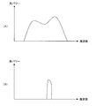
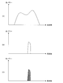
- (A) is a figure which shows an example of ASE light
- (B) is a figure which shows an example of a test signal.
- FIG. 1 It is a figure which shows an example of a structure of the optical transmission apparatus which concerns on a 3rd modification. It is a figure which shows an example of a structure of the optical transmission apparatus which concerns on a 4th modification. It is a figure which shows an example of a structure of the optical module which concerns on a 5th modification.
- A is a figure which shows an example of ASE light
- B is a figure which shows an example of the optical signal cut out by TF
- (C) is a figure which shows an example of a test signal.
- (A) is a figure which shows an example of ASE light
- (B) is a figure which shows an example of a test signal
- (C) is a figure which shows an example of the detection result in PD. It is a figure which shows an example of the other structure of the optical module which concerns on one Embodiment.
- FIG. 1 is a diagram illustrating an example of the configuration of an optical system according to an embodiment.
- An optical add-drop multiplexer (OADM) which is an example of an optical transmission apparatus, is provided in an optical node.
- the optical add / drop device has a function of adding (Add) an optical signal having one or a plurality of desired wavelengths to a WDM optical signal, and dropping an optical signal having one or a plurality of desired wavelengths from the WDM optical signal. It has a function to do.
- This optical add / drop device is also called an optical module or an optical package.
- the optical system shown in FIG. 1 (A) is a bidirectional ring network, and includes four optical nodes # 1 to # 4. That is, the optical nodes are connected by a pair of clockwise optical transmission lines and counterclockwise optical transmission lines. Each of the clockwise optical transmission line and the counterclockwise optical transmission line transmits a WDM optical signal. Each of the optical nodes # 1 to # 4 includes an optical add / drop multiplexer.
- An optical transmission line extending in a certain direction on the basis of each optical node or each optical add / drop multiplexer will be referred to as a “route”.
- the optical node # 1 (or the optical add / drop device of the optical node # 1) has a route # 1 and a route # 2.
- Route # 1 is connected to optical node # 4.
- an optical transmission path (incoming path) that transmits a WDM optical signal from the optical node # 4 to the optical node # 1
- a WDM optical signal is transmitted from the optical node # 1 to the optical node # 4.
- An optical transmission path (outbound path) is set.
- the route # 2 is connected to the optical node # 2.
- an optical transmission path (incoming path) that transmits a WDM optical signal from the optical node # 2 to the optical node # 1, and a WDM optical signal is transmitted from the optical node # 1 to the optical node # 2.
- An optical transmission path (outbound path) is set.
- the optical node # 1 when data is transmitted from the terminal station A to the terminal station B, the optical node # 1 outputs an optical signal transmitted from the terminal station A to the route # 1. At this time, the terminal station A transmits, for example, an optical signal carrying data using the wavelength ⁇ 1. Then, the optical add / drop multiplexer at the optical node # 1 transmits the optical signal transmitted from the terminal station A from the optical node # 2 to the optical node # 4 via the paths # 2 and # 1. Insert into. Then, the optical add / drop multiplexer at optical node # 4 branches the optical signal of wavelength ⁇ 1 from the WDM optical signal and guides it to the terminal station B. Thereby, the data transmitted from the terminal station A is received by the terminal station B.
- the terminal station C When transmitting data from the terminal station C to the terminal station A, the terminal station C transmits, for example, an optical signal that carries data using the wavelength ⁇ 2. Then, the optical add / drop multiplexer at the optical node # 2 transmits the optical signal transmitted from the terminal station C from the optical node # 3 to the optical node # 1 via the optical node # 2 and the route # 2. Insert into the optical signal. This WDM optical signal is input from the route # 2 to the optical node # 1. Then, the optical add / drop multiplexer at the optical node # 1 branches the optical signal of wavelength ⁇ 2 from the WDM optical signal and guides it to the terminal station A. Thereby, the data transmitted from the terminal station C is received by the terminal station A.
- each optical add / drop multiplexer has two paths, but it may have more paths.
- the optical add / drop multiplexer at optical node # 5 has four routes # 1 to # 4.
- the optical add / drop multiplexer at the optical node # 5 can output an optical signal of an arbitrary wavelength transmitted from the terminal station D to an arbitrary path.
- the optical add / drop multiplexer at the optical node # 5 can branch an optical signal of an arbitrary wavelength from an arbitrary path and transfer it to the terminal station D.
- FIG. 2 is a diagram illustrating an example of the configuration of an optical transmission device.
- the optical transmission device is also referred to as an optical add / drop device.
- the optical add / drop multiplexer 1 shown in FIG. 2 illustratively has n (n is an integer of 2 or more) paths.
- the n routes include, for example, two routes (WEST route (# 1) and EAST route (#n)) and a plurality of other routes (# 2 to # (n-1)). is doing.
- Each route includes a set of incoming and outgoing routes.
- the optical add / drop multiplexer 1 shown in FIG. 2 exemplarily has optical modules (packages) 2-1 to 2-2, 3 each having a functional block including a plurality of optical devices (optical elements) as one unit. -1 to 3-2, 4, 5-1 to 5-2 and 6-1 to 6-2, and the optical modules 2-1 to 2-2, 3-1 to 3-2, 4, 5-1 And a controller (processing unit) 7 for controlling 5-2 and 6-1 to 6-2.
- Each of the optical modules 2-1 and 2-2 includes a plurality of optical amplifiers.
- the optical modules 3-1 to 3-2 include a 1 ⁇ n wavelength selective optical switch (WSS), a 1 ⁇ n optical splitter (SPL: Splitter), and an optical splitter (SPL: Splitter), respectively. And an optical coupler (CPL: Coupler).
- each optical module 4 includes a plurality of optical amplifiers and a set of SPL and CPL.
- the optical modules 5-1 to 5-2 each include an optical cross-connect switch (OXC: Optical Cross Connect Switch) and a plurality of tunable filters (TF: Tunable Filter).
- each of the optical modules 6-1 to 6-2 includes a plurality of transponders (TPs).
- the optical modules 2-1 and 2-2 may be simply referred to as the optical module 2, and the optical modules 3-1 and 3-2 may be simply referred to as the optical module 3.
- the optical modules 5-1 and 5-2 may be simply referred to as the optical module 5
- the optical modules 6-1 and 6-2 may be simply referred to as the optical module 6.
- the optical module 2-1 amplifies the WDM optical signal input from the WEST route and amplifies the WDM optical signal output to the WEST route.
- the optical module 2-2 amplifies the WDM optical signal input from the EAST route and amplifies the WDM optical signal output to the EAST route.
- the gain of each optical amplifier in the optical modules 2-1 to 2-2 may be calculated in advance or may be dynamically controlled by the controller 7 or the like.
- the 1 ⁇ n SPL in the optical module 3-1 connected to the optical module 2-1 branches the WDM optical signal input from the WEST route, 1 ⁇ nWSS in module 3-2, SPL in optical module 3-1, and a plurality of other paths.
- the 1 ⁇ n SPL in the optical module 3-2 connected to the optical module 2-2 branches the WDM optical signal input from the EAST route, and 1 ⁇ nWSS, optical in the optical module 3-1. Lead to SPL and multiple other paths in module 3-2.
- the SPL in the optical module 3-1 branches the WDM optical signal guided from the 1 ⁇ n SPL in the optical module 3-1 and guides it to the optical amplifier in the optical module 4.
- the SPL in the optical module 3-2 branches the WDM optical signal guided from the 1 ⁇ n SPL in the optical module 3-2 and guides it to the optical amplifier in the optical module 4.
- the optical amplifier in the optical module 4 amplifies the optical signal input from the SPL in the optical module 3-1, and outputs it to the SPL in the optical module 4.
- the optical amplifiers in the other optical modules 4 amplify the optical signal input from the SPL in the optical module 3 and output it to the SPL in the optical module 4.
- the gain of each optical amplifier in the optical module 4 may be calculated in advance or may be dynamically controlled by the controller 7 or the like.
- the SPL in the optical module 4 branches the optical signal amplified by the optical amplifier in the optical module 4 and guides it to the OXC in the optical module 5-1.
- the OXC in each optical module 5-1 guides the input optical signal to an output port specified by the controller 7, for example.
- the TF in each optical module 5-1 passes only an optical signal having a wavelength specified by the controller 7, for example, among optical signals input from the OXC, while blocking optical signals having other wavelengths.
- the TP in the optical module 6-1 transfers the optical signal input from the TF in the optical module 5-1 to the corresponding terminal station.
- the wavelengths of the optical signals output from the TPs in the optical module 6-1 may be the same or different from each other.
- each TP in the optical module 6-2 transfers the optical signal transmitted from the corresponding terminal station to the TF in the optical module 5-2. .
- the wavelengths of the optical signals transmitted from the terminal stations may be the same or different from each other.
- the wavelength of the optical signal output from each TP in the optical module 6-2 is not particularly limited, but may be different from each other.
- Each TF in the optical module 5-2 passes, for example, only an optical signal having a wavelength specified by the controller 7 among optical signals input from each TP in the optical module 6-2. Block the optical signal.
- the OXC in the optical module 5-2 guides the optical signal input from the TF to an output port specified by the controller 7, for example.
- the CPL in the optical module 4 combines and outputs optical signals input from the OXC in the optical module 5-2. Further, the optical amplifier in the optical module 4 amplifies and outputs the optical signal input from the CPL.
- the gain of each optical amplifier in the optical module 4 may be calculated in advance or may be dynamically controlled by the controller 7 or the like.
- the CPL in the optical module 3-1 combines the optical signals input from the optical module 4 and outputs them to 1 ⁇ nWSS in the optical module 3-1.
- the CPL in the optical module 3-2 combines the optical signals input from the optical module 4 and outputs them to 1 ⁇ nWSS in the optical module 3-2.
- the 1 ⁇ nWSS in the optical module 3-1 is, for example, under the control of the controller 7, the optical signal guided from the EAST route via the 1 ⁇ nSPL in the optical module 3-2 and the optical module 3-1
- a WDM optical signal to be output to the WEST path is generated from the optical signal guided from the CPL and the optical signals input from the plurality of other paths.
- the 1 ⁇ nWSS in the optical module 3-1 is an optical signal guided from the EAST route via the 1 ⁇ nSPL in the optical module 3-2 and an optical signal input from the plurality of other paths. Then, one or a plurality of arbitrary wavelengths that “pass through” the optical add / drop multiplexer 1 are selected.
- the 1 ⁇ nWSS in the optical module 3-1 has one or more arbitrary wavelengths that are “inserted” into the WDM optical signal from the optical signal guided from the CPL in the optical module 3-1. select.
- the 1 ⁇ nWSS in the optical module 3-2 is an optical signal guided from the WEST route via the 1 ⁇ nSPL in the optical module 3-1, for example, under the control of the controller 7. 2 generates a WDM optical signal to be output to the EAST path from the optical signal guided from the CPL in 2 and the optical signals input from the plurality of other paths.
- the 1 ⁇ nWSS in the optical module 3-2 includes an optical signal guided from the WEST route via the 1 ⁇ nSPL in the optical module 3-1, and an optical signal input from the other plurality of routes. Then, one or a plurality of arbitrary wavelengths that “pass through” the optical add / drop multiplexer 1 are selected.
- the 1 ⁇ nWSS in the optical module 3-2 has one or more arbitrary wavelengths that are “inserted” into the WDM optical signal from the optical signal guided from the CPL in the optical module 3-2. select.
- the controller 7 controls each of the optical modules 2 to 6 in accordance with an instruction from a user or a network management device (not shown). For this reason, the controller 7 includes, for example, a processor and a memory.
- the memory may store a program describing the add operation and the drop operation of the optical add / drop multiplexer 1.
- the processor provides an add operation and a drop operation of the optical signal by executing a program stored in the memory.
- the controller 7 may provide an interface with a user or a network management device.
- optical fiber connection state determination method it is determined whether or not the optical fibers connecting the optical modules 2 to 6 in the optical add / drop multiplexer 1 illustrated in FIG. 2 are correctly connected.
- An example of a determination method optical fiber connection state determination method
- an optical signal transmission source modulates an optical signal at a different frequency for each optical fiber connection destination, and the modulated optical signal is transmitted to each optical fiber connection destination.
- PD photodetector
- optical signals that have been subjected to modulation processing of different frequencies are detected by photodetectors (PDs) arranged at respective connection destinations of optical fibers, and the modulation frequency of the received optical signal is determined based on the detection results. By detecting this, it is possible to confirm whether or not an optical signal is correctly transmitted from a desired transmission source. In the above method, it is desirable that the modulation applied to each optical signal is as gentle as not affecting the data superimposed on each optical signal.
- the number of optical fiber connections in the optical add / drop device 1 having the CDC function is very large.
- the optical add / drop device 1 capable of accommodating optical signals of 8 directions and 88 waves.
- hundreds to thousands of optical fibers may be used.
- the method as described above is applied to the optical add / drop device 1 and the modulators are arranged at all connection sources of the optical fibers and the photodetectors are arranged at all connection destinations of the optical fibers, The apparatus size and manufacturing cost of the apparatus 1 are increased.
- the optical add / drop multiplexer 1 having the CDC function when the path of each optical signal is incorrectly connected, a wavelength collision occurs, causing an error in the existing optical signal, or sending the optical signal to the wrong path. There is a possibility of doing. For this reason, when the method as described above is applied to the optical add / drop multiplexer 1, a modulation frequency of a type corresponding to the number of connected optical fibers is used. A sensitive photodetector (PD) is required, which also increases the size and manufacturing cost of the optical add / drop multiplexer 1.
- PD sensitive photodetector
- a method for easily determining the connection state of the optical fiber is proposed. Specifically, for example, a test signal for determining an optical fiber connection state is obtained by cutting out a part of amplified spontaneous emission (ASE) emitted from an optical amplifier or the like in the optical add / drop device 1. The generated test signal is connected to the optical fiber connecting the optical modules, and the optical fiber connection status is determined by determining whether the test signal is correctly detected at the receiving end (connection destination). Determine.
- the present invention is not limited to the application to the optical add / drop multiplexer 1 illustrated in FIG. 2, and can be applied to various optical fiber connection forms.
- FIG. 3 is an example of the configuration of an optical module for optical fiber connection state determination (hereinafter also simply referred to as an optical module) according to an embodiment.
- FIG. 3 is an example of the configuration of an optical module for optical fiber connection state determination (hereinafter also simply referred to as an optical module) according to an embodiment.
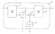
- the optical module 10 shown in FIG. 3 exemplarily includes a 1 ⁇ 2 optical coupler (CPL) 11, a wavelength tunable filter (TF) 12, a 1 ⁇ 2 optical coupler (CPL) 13, and a 2 ⁇ 1 optical switch. (SW) 14 and a photodetector (PD) 15.
- the optical module 10 is, for example, between the optical amplifier in the optical module 2-1 of the optical add / drop multiplexer 1 illustrated in FIG. 2 and the 1 ⁇ n SPL in the optical module 3-1, or in the optical module 2-2. It is desirable to be disposed between the optical amplifier and the 1 ⁇ nSPL in the optical module 3-2.
- ASE light emitted from the optical amplifiers in the optical modules 2-1 to 2-2 can be input to the optical module 10.
- the optical module 10 is arranged between the optical amplifier in the optical module 4 and the CPL in the optical module 3-1, or between the optical amplifier in the optical module 4 and the CPL in the optical module 3-2. May be.
- the 1 ⁇ 2 CPL 11 branches the input light and guides it to the subsequent 2 ⁇ 1 SW 14 and the TF 12.
- the input light includes ASE light input from the preceding optical amplifier and main signal light input during operation of the optical system.
- the TF 12 passes only an optical signal having a predetermined wavelength among optical signals input from the 1 ⁇ 2 CPL 11, while blocking optical signals having other wavelengths. Note that the wavelength that the TF 12 passes may be controlled by the controller 7 or the like, for example.
- the TF 12 generates a test signal for determining an optical fiber connection state by cutting out ASE light corresponding to one wave of the optical signal propagating through the optical system.
- the test signal generated by the TF 12 is output to the 1 ⁇ 2 CPL 13.
- the TF 12 cuts out a part of the input ASE light, so that the wavelength corresponding to the wavelength of the optical signal receivable at the connection destination (reception end) among the connection destinations (multiple reception ends) of the optical fiber is changed. It functions as an example of a wavelength tunable filter that generates a test signal.
- the 1 ⁇ 2 CPL 13 branches the test signal generated by the TF 12 and guides it to the 2 ⁇ 1 SW 14 and the PD 15.
- 2 ⁇ 1 SW 14 selects and outputs one of the optical signal input from 1 ⁇ 2 CPL 11 and the optical signal input from 1 ⁇ 2 CPL 13.
- the 2 ⁇ 1 SW 14 receives an optical signal (that is, the test signal) input from the 1 ⁇ 2 CPL 13 when determining the optical fiber connection state, for example, when the optical add / drop device 1 is started up or when a new channel is started up.
- an optical signal that is, main signal light
- the selection operation of the 2 ⁇ 1 SW 14 may be controlled by the controller 7 or the like, for example.
- the 2 ⁇ 1 SW 14 functions as an example of an optical output unit that outputs a test signal generated by the TF 12.
- the PD 15 detects the optical power of the test signal that is branched and input by the 1 ⁇ 2 CPL 13. The detection result is notified to, for example, the controller 7 and used for amplification gain control for the optical amplifier in the optical add / drop multiplexer 1 and passband control of the TF 12. That is, the optical power of the test signal can be controlled to a desired value.
- the test signal generated by cutting out a part of the ASE light by the optical module 10 having the above configuration is used as a photodetector (PD) provided at the optical fiber connection end of each of the optical modules 2 to 6. And based on the detection result, it is determined whether or not each optical fiber connection is valid.
- PD photodetector
- an optical fiber connection state determination process triggered by activation of the optical add / drop multiplexer 1 or startup of a new channel, etc. Is started (step S10), ASE light is emitted from the optical amplifier in the optical add / drop multiplexer 1 (step S11).
- the 1 ⁇ 2 CPL 11 in the optical module 10 arranged at the rear stage of the optical amplifier in the optical add / drop device 1 branches the ASE light input from the optical amplifier and guides it to the TF 12.
- the TF 12 is for determining an optical fiber connection state by cutting out an optical signal having a wavelength corresponding to the wavelength of an optical signal branched (dropped) by the optical add / drop multiplexer 1 from the ASE light input from the 1 ⁇ 2 CPL 11. Generate a test signal. Note that the optical power of the test signal can be increased or decreased by the controller 7 or the like based on the detection result of the PD 15. At this time, the 2 ⁇ 1 SW 14 selects and outputs the input (that is, the test signal) from the 1 ⁇ 2 CPL 13 out of the input from the 1 ⁇ 2 CPL 11 and the input from the 1 ⁇ 2 CPL 13 (step S12).
- the 2 ⁇ 1 SW 14 is the input from the 1 ⁇ 2 CPL 11 (that is, the main input from the input from the 1 ⁇ 2 CPL 11 and the input from the 1 ⁇ 2 CPL 13). (Signal light) is selected and output.
- the optical module 10 is disposed between an optical amplifier that amplifies an optical signal input from the WEST path among the optical amplifiers in the optical module 2-1, and 1 ⁇ nSPL in the optical module 3-1.
- the optical fiber connection state determination method of this example will be described.
- the test signal generated and output by the optical module 10 is input to the optical module 3-1 via an optical fiber connecting the optical module 10 and the optical module 3-1.
- the test signal is branched by 1 ⁇ nSPL in the optical module 3-1, and then branched by SPL in the optical module 3-1, and connects between the optical module 3-1 and the optical module 4.
- the signal is input to the optical module 4 through the optical fiber.
- the controller 7 determines whether or not the test signal is detected at a desired level in the photodetector (drop-side PD) disposed at the receiving end of the optical amplifier disposed in the preceding stage of the SPL in the optical module 4. (Step S13).
- the desired level refers to the optical power of the test signal whose gain is controlled by the PD 15 and the controller 7 in the optical module 10.
- the controller 7 determines at least the test signal among the optical fiber connections between the optical module 3-1 and the optical module 4. It can be determined that the optical fiber that propagates is correctly connected.
- the controller 7 at least performs the test among the optical fiber connections between the optical module 3-1 and the optical module 4. It is determined that the optical fiber through which the signal propagates is not properly connected, and it is possible to notify the network management device or the like that the optical fiber is erroneously connected or that the optical fiber is disconnected (step S14). Thereby, the erroneous connection of the optical fiber or the disconnection of the optical fiber can be corrected by a network administrator or a user.
- the controller 7 determines that the optical fiber is erroneously connected when the optical signal detection result of the test signal is smaller than the predetermined threshold, while the optical power detection result of the test signal is greater than or equal to the predetermined threshold. In some cases, it may be determined that the optical fiber is correctly connected. Of the optical fiber connections between the optical module 3-1 and the optical module 4, if at least the optical fiber through which the test signal propagates is correctly connected, then the controller 7 It is determined whether or not the test signal is detected at a desired level in the photodetector (PD) disposed at the receiving end of the OXC (step S15).
- PD photodetector
- the controller 7 determines that the optical module 4 and the optical module Among the optical fiber connections with 5-1, it can be determined that at least the optical fiber through which the test signal propagates is correctly connected.
- step S15 when the test signal cannot be detected at a desired level in the photodetector (PD) disposed at the receiving end of the OXC in the optical module 5-1, (No route in step S15), the controller 7 Of the optical fiber connections with the optical module 5-1, it is determined that at least the optical fiber through which the test signal propagates is not correctly connected, and that the optical fiber is misconnected or the optical fiber is disconnected. A notification can be sent to the network management device or the like (step S16). Thereby, the erroneous connection of the optical fiber or the disconnection of the optical fiber can be corrected by a network administrator or a user.
- PD photodetector
- the controller 7 determines that the optical fiber is erroneously connected when the optical signal detection result of the test signal is smaller than the predetermined threshold, while the optical power detection result of the test signal is greater than or equal to the predetermined threshold. In some cases, it may be determined that the optical fiber is correctly connected. Of the optical fiber connections between the optical module 4 and the optical module 5-1, if at least the optical fiber through which the test signal propagates is correctly connected, then the controller 7 It is determined whether or not the test signal is detected at a desired level in the photodetector (PD) disposed at the receiving end of the TP (step S17).
- PD photodetector
- the controller 7 determines that the optical module 5-1 Among the optical fiber connections with the optical module 6-1, it can be determined that at least the optical fiber through which the test signal propagates is correctly connected. In this case, it can also be confirmed that the transmission wavelength setting of the TF in the optical module 5-1 is appropriate.
- the controller 7 determines that the optical module 5- It is determined that at least the optical fiber through which the test signal propagates is not correctly connected among the optical fiber connections between 1 and the optical module 6-1, and the optical fiber is erroneously connected or the optical fiber is disconnected. This can be notified to the network management device or the like (step S18). Thereby, the erroneous connection of the optical fiber or the disconnection of the optical fiber can be corrected by a network administrator or a user.
- the controller 7 determines that the optical fiber is erroneously connected when the optical signal detection result of the test signal is smaller than the predetermined threshold, while the optical power detection result of the test signal is greater than or equal to the predetermined threshold. In some cases, it may be determined that the optical fiber is correctly connected.
- the controller 7 then changes the transmission wavelength of the TF 12 (step S19), and the steps S13 to S18. Repeat the process. For example, the controller 7 changes the transmission wavelength of the TF 12 so as to transmit other wavelengths of the optical signal branched (dropped) by the optical add / drop device 1.
- the controller 7 may end the optical fiber determination process.
- a part of the optical fiber connection state determination process corresponding to the connection part may be omitted.
- the optical module 10 is connected between the optical amplifier that amplifies an optical signal input from the WEST path among the optical amplifiers in the optical module 2-1, and 1 ⁇ nSPL in the optical module 3-1.
- the validity of each optical fiber connection in the drop direction between the optical modules 3-1, 4, 5-1, and 6-1 was determined.
- the optical module 10 is installed in the optical module 2-2. If the optical amplifier is disposed between the optical amplifier that amplifies the optical signal input from the EAST path and the 1 ⁇ nSPL in the optical module 3-2, the optical modules 3-2, 4, 5-1 and The validity of each optical fiber connection in the drop direction between 6-1 can be similarly determined.
- the optical module 10 is disposed between the optical amplifier in the optical module 4 and the CPL in the optical module 3-1 (or 3-2), the optical modules 4 and 3-1 (or 3-2) are provided.
- the validity of each optical fiber connection in the add direction can be similarly determined. As described above, according to this example, it is possible to easily determine the connection state of the optical fiber.
- optical module 10A as illustrated in FIG. 6 may be used.
- the optical module 10 ⁇ / b> A includes 1 ⁇ 2 SW 16 instead of 1 ⁇ 2 CPL 11. 6 having the same reference numerals as those in FIG. 3 have the same functions as the components shown in FIG.
- 1 ⁇ 2 SW 16 selectively outputs an optical signal input from an input port from any output port.
- the 1 ⁇ 2 SW 16 outputs the input light to the route of the TF 12 when determining the optical fiber connection state such as when the optical add / drop multiplexer 1 is started up or when a new channel is started up.
- the input light is output to the 2 ⁇ 1 SW 14 route.
- the selection operation of the 1 ⁇ 2 SW 16 may be controlled by the controller 7 or the like, for example.
- the optical module 20 illustrated in FIG. 7 includes, for example, an ASE light source 21, a TF 22, a 1 ⁇ 2 CPL 23, a 2 ⁇ 1 SW 24, and a PD 25.
- the ASE light source 21 outputs ASE light as illustrated in FIG.
- the TF 22 passes only an optical signal having a predetermined wavelength out of ASE light input from the ASE light source 21, while blocking optical signals having other wavelengths. Note that the wavelength that the TF 22 passes may be controlled by the controller 7 or the like, for example.
- the TF 22 generates a test signal for determining an optical fiber connection state by cutting out ASE light corresponding to one wave of the optical signal propagating through the optical system.
- the test signal generated by the TF 22 is output to the 1 ⁇ 2 CPL 23.
- the 1 ⁇ 2 CPL 23 branches the test signal generated by the TF 22 and guides it to the 2 ⁇ 1 SW 24 and the PD 25.
- the 2 ⁇ 1 SW 24 selects and outputs either an optical signal input from the outside or an optical signal input from the 1 ⁇ 2 CPL 23.
- the 2 ⁇ 1 SW 24 receives an optical signal (that is, the test signal) input from the 1 ⁇ 2 CPL 23 at the time of determining the optical fiber connection state such as when the optical add / drop device 1 is started up or when a new channel is started up.
- an optical signal input from the outside that is, main signal light
- the 2 ⁇ 1 SW 24 selection operation may be controlled by the controller 7 or the like, for example.
- the PD 25 detects the optical power of the test signal that is branched and input by the 1 ⁇ 2 CPL 23.
- the detection result is notified to, for example, the controller 7 and used for amplification gain control for the optical amplifier in the optical add / drop multiplexer 1 and passband control for the TF 22. That is, the optical power of the test signal can be controlled to a desired value. If the optical module 20 configured as described above is disposed, for example, before the TP in the optical module 6-2, the optical modules 6-2, 5-2, 4 and 3-1 (or 3-2) The validity of each optical fiber connection in the add direction can be similarly determined.
- FIG. 8 is a diagram illustrating an example of a configuration of an optical add / drop multiplexer 1A according to a third modification.
- the optical add / drop device 1A shown in FIG. 8 exemplarily shows optical modules (packages) 2A-1 to 2A-6, 3A- each having a functional block including a plurality of optical devices (optical elements) as one unit. 1 to 3A-2, 4A, 5A and 6A-1 to 6A-2, and optical modules 2A-1 to 2A-6, 3A-1 to 3A-2, 4A, 5A and 6A-1 to 6A-2 And a controller 7A for controlling.
- each of the optical modules 2A-1 to 2A-6, 3A-1 to 3A-2, 4A, 5A and 6A in the optical add / drop multiplexer 1A are used. It is assumed that a photodetector (PD) capable of detecting the optical power of input light is disposed at the receiving ends (optical fiber connection destinations) of -1 to 6A-2 (shaded circles in FIG. 8) See sign). Also in the optical add / drop device 1A illustrated in FIG. 8, each of the optical modules 2A-1 to 2A-6, 3A is provided if at least one of the optical modules 10, 10A, and 20 described above is disposed at an appropriate position. The validity of each optical fiber connection between -1 to 3A-2, 4A, 5A and 6A-1 to 6A-2 can be easily determined.
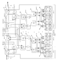
- FIG. 9 is a diagram illustrating an example of a configuration of an optical add / drop multiplexer 1B according to a fourth modification.
- the optical add / drop device 1B shown in FIG. 9 exemplarily shows optical modules (packages) 2B-1 to 2B-2, 3B- each having a functional block including a plurality of optical devices (optical elements) as one unit.
- each optical module 2B-1 to 2B-2, 3B-1 to 3B-2, 4B, 5B, 6B in the optical add / drop multiplexer 1B is used.
- 8B, 9B and 10B-1 to 10B-2 are provided with photodetectors (PDs) capable of detecting the optical power of the input light at the receiving ends (connection destinations of optical fibers) (see FIG. (See the shaded circle in 9).
- PDs photodetectors
- the optical modules 2B-1 to 2B-2, 3B are provided.
- the validity of each optical fiber connection between -1 to 3B-2, 4B, 5B, 6B, 8B, 9B and 10B-1 to 10B-2 can be easily determined. It is also possible to determine an operation error such as a wavelength selection setting error in each WSS or a failure of each WSS itself.
- the validity of the optical fiber connection and the route setting of each optical signal are determined by modulating the test signal and detecting the test signal power level and modulation frequency together. can do. That is, even when an optical signal having a wavelength different from the receivable optical signal is input at the receiving end, the connection state of the optical fiber is determined based on the modulation frequency of the modulation applied to the input light. Can do.
- FIG. 10 is a diagram illustrating an example of a configuration of an optical module according to a fifth modification.
- the optical module 30 shown in FIG. 10 includes, for example, a 1 ⁇ 2 CPL 31, a TF 32, a modulator 33, a 1 ⁇ 2 CPL 34, a 2 ⁇ 1 SW 35, and a PD 36.
- the 1 ⁇ 2 CPL 31 branches the input light and guides it to the subsequent 2 ⁇ 1 SW 35 and the TF 32.
- the input light includes ASE light input from an optical amplifier at the previous stage and main signal light input during operation of the optical system.
- the TF 32 allows only an optical signal having a predetermined wavelength among optical signals input from the 1 ⁇ 2 CPL 31 to pass therethrough, and blocks optical signals having other wavelengths.
- the wavelength that the TF 32 passes may be controlled by the controller 7 or the like, for example.
- ASE light having a frequency-to-optical power characteristic as illustrated in FIG. At this time, the TF 32 cuts out ASE light corresponding to one wave of the optical signal propagating through the optical system, as illustrated in FIG.
- the optical signal cut out by the TF 32 is output to the modulator 33.
- the modulator 33 modulates the optical signal cut out by the TF 32 with a predetermined modulation frequency.
- the modulation frequency for the modulation performed by the modulator 33 may be controlled by the controller 7 or the like, for example.
- a ferroelectric crystal such as LiNbO3 (lithium niobate) may be used.
- an optical signal as illustrated in FIG. 11B is input to the modulator 33.
- the modulator 33 modulates the input optical signal using a predetermined modulation frequency to generate a test signal for determining the optical fiber connection state.
- the test signal generated by the modulator 33 is output to the 1 ⁇ 2 CPL 34.
- the 1 ⁇ 2 CPL 34 branches the test signal generated by the TF 32 and the modulator 33 and guides it to the 2 ⁇ 1 SW 35 and the PD 36.
- the 2 ⁇ 1 SW 35 selects and outputs either the optical signal input from the 1 ⁇ 2 CPL 31 or the optical signal input from the 1 ⁇ 2 CPL 34.
- the 2 ⁇ 1 SW 35 receives an optical signal (that is, the test signal) input from the 1 ⁇ 2 CPL 34 at the time of determining the optical fiber connection state such as when the optical add / drop device 1 is started up or when a new channel is started up.
- an optical signal that is, main signal light
- the selection operation of the 2 ⁇ 1 SW 35 may be controlled by the controller 7 or the like, for example.
- the PD 36 detects the optical power and modulation frequency of the test signal that is branched and input by the 1 ⁇ 2 CPL 34.
- the detection result is notified to, for example, the controller 7 and used for amplification gain control for the optical amplifier in the optical add / drop multiplexer 1, passband control for the TF 32, modulation frequency control for the modulator 33, and the like. That is, the optical power and the modulation frequency of the test signal can be controlled to desired values, respectively.
- the test signal generated by the optical module 30 having the above-described configuration is detected by a photodetector (PD) provided at the optical fiber connection end of each of the optical modules 2 to 6, and each optical fiber is detected based on the detection result. It can be determined whether the connection is valid. Specifically, for example, when the controller 7 matches the detection result of the modulation frequency of the test signal with a predetermined modulation frequency and the detection result of the optical power of the test signal is equal to or greater than a predetermined threshold, the optical fiber If the detection result of the modulation frequency of the test signal does not match the predetermined modulation frequency or the detection result of the optical power of the test signal is smaller than the predetermined threshold, the optical fiber Can be determined to be misconnected.
- PD photodetector
- the optical module 30 is disposed between the optical amplifier in the optical module 2-1 and the 1 ⁇ nSPL in the optical module 3-1, and the optical module Even when the optical module 30 is arranged between the optical amplifier in 2-2 and 1 ⁇ nSPL in the optical module 3-2, the modulation frequency in each modulator 33 is set to a different value. Since it is possible to identify from which optical module 30 each test signal is transmitted in each PD, it is possible to easily determine the validity of the route setting of each optical signal.
- an optical module 30A as illustrated in FIG. 12 may be used.
- the optical module 30 ⁇ / b> A includes a 1 ⁇ 2 SW 37 instead of the 1 ⁇ 2 CPL 31. 12 having the same reference numerals as those in FIG. 10 have the same functions as the components shown in FIG.
- the 1 ⁇ 2 SW 37 selectively outputs an optical signal input from the input port from any output port.
- the 1 ⁇ 2 SW 37 outputs input light to the route of the TF 32 at the time of optical fiber connection state determination such as when the optical add / drop device 1 is started up or when a new channel is started up.
- the input light is output to the 2 ⁇ 1SW 35 route.
- the selection operation of the 1 ⁇ 2 SW 37 may be controlled by the controller 7 or the like, for example.
- an optical module 40 as illustrated in FIG. 13 may be used.
- the optical module 40 shown in FIG. 13 includes, for example, an ASE light source 41, a TF 42, a modulator 43, a 1 ⁇ 2 CPL 44, a 2 ⁇ 1 SW 45, and a PD 46.
- the ASE light source 41 outputs ASE light as illustrated in FIG.
- the TF 42 passes only an optical signal having a predetermined wavelength out of the ASE light input from the ASE light source 41, while blocking optical signals having other wavelengths.
- the wavelength that the TF 42 passes may be controlled by the controller 7 or the like, for example.
- the TF 42 cuts out ASE light corresponding to one wave of the optical signal propagating through the optical system.
- the optical signal cut out by the TF 42 is output to the modulator 43.
- the modulator 43 modulates the optical signal cut out by the TF 42 with a predetermined modulation frequency.
- the modulation frequency for the modulation performed by the modulator 43 may be controlled by the controller 7 or the like, for example.
- a ferroelectric crystal such as LiNbO3 (lithium niobate) may be used.
- the modulator 43 generates a test signal for determining an optical fiber connection state by modulating the input optical signal using a predetermined modulation frequency. .
- the test signal generated by the modulator 43 is output to the 1 ⁇ 2 CPL 44.
- the 1 ⁇ 2 CPL 44 branches the test signal generated by the TF 42 and the modulator 43 and guides it to the 2 ⁇ 1 SW 45 and the PD 46.
- the 2 ⁇ 1 SW 45 selects and outputs either an optical signal input from the outside or an optical signal input from the 1 ⁇ 2 CPL 44.
- the 2 ⁇ 1 SW 45 receives an optical signal input from the 1 ⁇ 2 CPL 44 (that is, the above test signal) at the time of determining the optical fiber connection state such as when the optical add / drop device 1 is started up or when a new channel is started up.
- an optical signal input from the outside that is, main signal light
- the selection operation of the 2 ⁇ 1 SW 45 may be controlled by the controller 7 or the like, for example.
- the PD 46 detects the optical power and modulation frequency of the test signal that is branched and input by the 1 ⁇ 2 CPL 44.
- the detection result is notified to, for example, the controller 7 and used for amplification gain control for the optical amplifier in the optical add / drop multiplexer 1, passband control for the TF 42, modulation frequency control for the modulator 43, and the like. That is, the optical power and the modulation frequency of the test signal can be controlled to desired values, respectively.
- the optical module 40 configured as described above is disposed, for example, before the TP in the optical module 6-2, the optical modules 6-2, 5-2, 4 and 3-1 (or 3-2)
- the validity of each optical fiber connection in the add direction can be similarly determined.
- the modulation frequency in each modulator 43 is changed. If different values are set, it is possible to identify from which optical module 40 each test signal is transmitted in each PD. Therefore, it is possible to easily determine the validity of the route setting of each optical signal. Is possible.
- the TFs 12, 22, 32, and 42 in each of the optical modules 10, 10A, 20, 30, 30A, and 40 can arbitrarily change the bandwidth of the test signal cut out from the ASE light. Is possible.
- a pseudo signal (test signal) corresponding to a high-speed, wide-band optical signal such as 400 Gbps or 1 Tbps can be generated.
- the optical module 10 includes an optical amplifier that amplifies an optical signal input from the WEST path among the optical amplifiers in the optical module 2B-1, and the optical module 3B-. It is arranged between WSSs in 1.
- the optical module 10 detects a pseudo signal (test) corresponding to a high-speed, wide-band optical signal such as 400 Gbps and 1 Tbps as illustrated in FIG. 14B from ASE light as illustrated in FIG. Signal).
- a pseudo signal test
- each PD in each of the optical modules 4B, 6B, 9B and 10B-1 detects the optical power of the test signal generated by the optical module 10.
- any of the optical modules 4B, 6B, 9B and 10B-1 if there is a setting error regarding the wavelength band, the test signal input to each PD has a waveform as illustrated in FIG. 14C. It will have. For this reason, when the optical power detected in each PD is lower than a desired level, there is an erroneous connection in the optical fiber connecting the optical modules 4B, 6B, 9B, and 10B-1, or each optical module It can be determined that there is a setting error regarding the wavelength band in 4B, 6B, 9B, and 10B-1.
- the system operation can be performed while the optical modules 10, 10A, 20, 30, 30A, and 40 are interposed between the optical module 2-1 and the optical module 3-1.
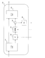
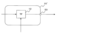
- the optical module 10 ′ having the configuration illustrated in FIG. 15 may be interposed between the optical module 2-1 and the optical module 3-1 only during the optical fiber connection state determination process.
- the optical module 10 ′ cuts out at least a part of the input ASE light, so that an optical signal that can be received by one of the plurality of receiving ends is received. What is necessary is just to provide TF12 which produces
- any one of the controllers 7, 7A, and 7B functions as an example of a processing unit that determines the connection state of the optical fiber based on the detection result of each PD. , 20, 30, 30A and 40 may separately have the same processing unit.
Landscapes
- Physics & Mathematics (AREA)
- Engineering & Computer Science (AREA)
- Computer Networks & Wireless Communication (AREA)
- Signal Processing (AREA)
- Electromagnetism (AREA)
- Optics & Photonics (AREA)
- Chemical & Material Sciences (AREA)
- Analytical Chemistry (AREA)
- General Physics & Mathematics (AREA)
- Optical Communication System (AREA)
- Testing Of Optical Devices Or Fibers (AREA)
Abstract
Selon la présente invention, afin de déterminer l'état de connexion d'une fibre optique qui connecte une borne d'émission et une pluralité de bornes de réception, un signal d'essai ayant une longueur d'onde correspondant à la longueur d'onde d'un signal optique apte à être reçu à l'une des bornes de réception de la pluralité de bornes de réception est généré au moyen de la coupe d'une partie d'une lumière d'émission spontanée amplifiée, le signal d'essai généré est transmis à la fibre optique, la puissance optique du signal d'essai est détectée par la première borne de réception, et l'état de connexion de fibre optique est déterminé sur la base des résultats de détection pour la puissance optique du signal d'essai.
Priority Applications (3)
| Application Number | Priority Date | Filing Date | Title |
|---|---|---|---|
| PCT/JP2012/064692 WO2013183146A1 (fr) | 2012-06-07 | 2012-06-07 | Procédé de détermination d'état de connexion de fibre optique, module optique de détermination d'état de connexion de fibre optique et dispositif d'émission optique |
| JP2014519766A JP5896022B2 (ja) | 2012-06-07 | 2012-06-07 | 光ファイバ接続状態判定方法、光ファイバ接続状態判定用光モジュール及び光伝送装置 |
| US14/560,500 US20150086192A1 (en) | 2012-06-07 | 2014-12-04 | Determining method, determining optical module, and optical communication apparatus |
Applications Claiming Priority (1)
| Application Number | Priority Date | Filing Date | Title |
|---|---|---|---|
| PCT/JP2012/064692 WO2013183146A1 (fr) | 2012-06-07 | 2012-06-07 | Procédé de détermination d'état de connexion de fibre optique, module optique de détermination d'état de connexion de fibre optique et dispositif d'émission optique |
Related Child Applications (1)
| Application Number | Title | Priority Date | Filing Date |
|---|---|---|---|
| US14/560,500 Continuation US20150086192A1 (en) | 2012-06-07 | 2014-12-04 | Determining method, determining optical module, and optical communication apparatus |
Publications (1)
| Publication Number | Publication Date |
|---|---|
| WO2013183146A1 true WO2013183146A1 (fr) | 2013-12-12 |
Family
ID=49711563
Family Applications (1)
| Application Number | Title | Priority Date | Filing Date |
|---|---|---|---|
| PCT/JP2012/064692 Ceased WO2013183146A1 (fr) | 2012-06-07 | 2012-06-07 | Procédé de détermination d'état de connexion de fibre optique, module optique de détermination d'état de connexion de fibre optique et dispositif d'émission optique |
Country Status (3)
| Country | Link |
|---|---|
| US (1) | US20150086192A1 (fr) |
| JP (1) | JP5896022B2 (fr) |
| WO (1) | WO2013183146A1 (fr) |
Cited By (5)
| Publication number | Priority date | Publication date | Assignee | Title |
|---|---|---|---|---|
| WO2017022231A1 (fr) * | 2015-08-03 | 2017-02-09 | 日本電気株式会社 | Dispositif de multiplexage à insertion/extraction optique et procédé de multiplexage à insertion/extraction optique |
| WO2020217439A1 (fr) * | 2019-04-26 | 2020-10-29 | 三菱電機株式会社 | Dispositif de communication optique |
| CN112054840A (zh) * | 2019-06-06 | 2020-12-08 | 中国移动通信有限公司研究院 | 连接信息发送方法、接收方法、光模块和中心处理设备 |
| WO2021060124A1 (fr) | 2019-09-27 | 2021-04-01 | 日本電気株式会社 | Système de communication optique, dispositif de communication optique, procédé de communication optique, et support d'informations |
| JP2024536854A (ja) * | 2021-09-26 | 2024-10-08 | 中興通訊股▲ふん▼有限公司 | 光ファイバー検出方法、roadmシステム、サーバ及び記憶媒体 |
Families Citing this family (2)
| Publication number | Priority date | Publication date | Assignee | Title |
|---|---|---|---|---|
| US11838101B2 (en) * | 2018-01-26 | 2023-12-05 | Ciena Corporation | Upgradeable colorless, directionless, and contentionless optical architectures |
| US10608774B2 (en) | 2018-07-27 | 2020-03-31 | At&T Intellectual Property I, L.P. | Network switch and optical transponder connectivity verification for wavelength division multiplexing network |
Citations (5)
| Publication number | Priority date | Publication date | Assignee | Title |
|---|---|---|---|---|
| JP2002057394A (ja) * | 2000-08-14 | 2002-02-22 | Fujitsu Ltd | 光増幅装置および光増幅方法ならびに光通信システム |
| JP2005341529A (ja) * | 2004-04-28 | 2005-12-08 | Fujitsu Ltd | 光伝送システム,光送受信装置,光伝送装置および光波長チャンネル接続認識制御方法 |
| JP2006135651A (ja) * | 2004-11-05 | 2006-05-25 | Fujitsu Ltd | 光通信装置の光出力自動減衰回路 |
| JP2008288993A (ja) * | 2007-05-18 | 2008-11-27 | Mitsubishi Electric Corp | 接続状態検出方法および通信システム |
| JP2012015726A (ja) * | 2010-06-30 | 2012-01-19 | Fujitsu Ltd | 光分岐挿入装置 |
Family Cites Families (26)
| Publication number | Priority date | Publication date | Assignee | Title |
|---|---|---|---|---|
| US7046929B1 (en) * | 1999-08-24 | 2006-05-16 | Ciena Corporation | Fault detection and isolation in an optical network |
| JP3813063B2 (ja) * | 2001-02-01 | 2006-08-23 | 富士通株式会社 | 通信システム及び波長分割多重装置 |
| US7076164B2 (en) * | 2001-06-22 | 2006-07-11 | Tellabs Operations, Inc. | System and method for measuring power of optical signals carried over a fiber optic link |
| US6765659B1 (en) * | 2002-08-30 | 2004-07-20 | Ciena Corporation | Optical supervisory channel apparatus and method for measuring optical properties |
| US7561798B2 (en) * | 2003-03-07 | 2009-07-14 | Verizon Services Corp. | Testing a fiber link in a communication system without interrupting service |
| US7389045B2 (en) * | 2003-05-08 | 2008-06-17 | Verizon Business Global Llc | Apparatus and method for monitoring and compensating an optical signal |
| US7274872B2 (en) * | 2004-03-12 | 2007-09-25 | Futurewei Technologies, Inc. | System and method for subcarrier modulation as supervisory channel |
| IES20040413A2 (en) * | 2004-06-18 | 2005-12-29 | Intune Technologies Ltd | Method and system for a distributed wavelength (lambda) routed (dlr) network |
| US7542678B2 (en) * | 2004-12-30 | 2009-06-02 | Alcatel-Lucent Usa Inc. | Method and apparatus for a supervisory channel in a WDM fiber-optic communication system |
| JP4252610B2 (ja) * | 2005-03-01 | 2009-04-08 | 富士通株式会社 | 伝送装置、伝送装置試験方法および伝送装置試験プログラム |
| KR100698766B1 (ko) * | 2005-09-07 | 2007-03-23 | 한국과학기술원 | 파장분할 다중방식 수동형 광 가입자 망 시스템에 사용되는장애 위치 감시 장치 및 이를 구비한 파장분할 다중방식수동형 광 가입자 망 시스템 |
| US7526198B1 (en) * | 2005-11-30 | 2009-04-28 | At&T Corp. | Methods of restoration in an ultra-long haul optical network |
| JP4699924B2 (ja) * | 2006-03-16 | 2011-06-15 | 富士通株式会社 | 光特性を測定する方法およびシステム |
| WO2008114438A1 (fr) * | 2007-03-20 | 2008-09-25 | Fujitsu Limited | Procédé et dispositif de surveillance de ligne de transmission |
| JP5040813B2 (ja) * | 2008-05-28 | 2012-10-03 | 富士通株式会社 | 光分岐挿入多重化装置 |
| US20100239245A1 (en) * | 2009-03-21 | 2010-09-23 | General Photonics Corporation | Polarization Mode Emulators and Polarization Mode Dispersion Compensators Based on Optical Polarization Rotators with Discrete Polarization States |
| US8811815B2 (en) * | 2009-04-20 | 2014-08-19 | Verizon Patent And Licensing Inc. | Optical network testing |
| US8494360B2 (en) * | 2009-04-24 | 2013-07-23 | Verizon Patent And Licensing Inc. | In-service optical network testing |
| US8254788B2 (en) * | 2009-12-14 | 2012-08-28 | Verizon Patent And Licensing, Inc. | High speed in-service optical network testing |
| US8718475B2 (en) * | 2010-03-19 | 2014-05-06 | Telcordia Technologies, Inc. | Transponder pool sizing in highly dynamic translucent WDM optical networks |
| JP5471670B2 (ja) * | 2010-03-19 | 2014-04-16 | 富士通株式会社 | 光ノード、光ネットワークシステムおよび偏波モード分散測定方法 |
| US9246580B2 (en) * | 2010-06-24 | 2016-01-26 | Mitsubishi Electric Corporation | Optical add-drop multiplexer (OADM) device |
| JP5614252B2 (ja) * | 2010-11-12 | 2014-10-29 | 富士通株式会社 | 光切替装置および通信システム |
| JP2012244530A (ja) * | 2011-05-23 | 2012-12-10 | Fujitsu Ltd | ファイバ誤接続検出方法及びノード装置 |
| JP5776330B2 (ja) * | 2011-05-25 | 2015-09-09 | 富士通株式会社 | 波長再配置方法及びノード装置 |
| JP2013005113A (ja) * | 2011-06-14 | 2013-01-07 | Nec Corp | 光チャネルモニタ |
-
2012
- 2012-06-07 WO PCT/JP2012/064692 patent/WO2013183146A1/fr not_active Ceased
- 2012-06-07 JP JP2014519766A patent/JP5896022B2/ja not_active Expired - Fee Related
-
2014
- 2014-12-04 US US14/560,500 patent/US20150086192A1/en not_active Abandoned
Patent Citations (5)
| Publication number | Priority date | Publication date | Assignee | Title |
|---|---|---|---|---|
| JP2002057394A (ja) * | 2000-08-14 | 2002-02-22 | Fujitsu Ltd | 光増幅装置および光増幅方法ならびに光通信システム |
| JP2005341529A (ja) * | 2004-04-28 | 2005-12-08 | Fujitsu Ltd | 光伝送システム,光送受信装置,光伝送装置および光波長チャンネル接続認識制御方法 |
| JP2006135651A (ja) * | 2004-11-05 | 2006-05-25 | Fujitsu Ltd | 光通信装置の光出力自動減衰回路 |
| JP2008288993A (ja) * | 2007-05-18 | 2008-11-27 | Mitsubishi Electric Corp | 接続状態検出方法および通信システム |
| JP2012015726A (ja) * | 2010-06-30 | 2012-01-19 | Fujitsu Ltd | 光分岐挿入装置 |
Cited By (11)
| Publication number | Priority date | Publication date | Assignee | Title |
|---|---|---|---|---|
| WO2017022231A1 (fr) * | 2015-08-03 | 2017-02-09 | 日本電気株式会社 | Dispositif de multiplexage à insertion/extraction optique et procédé de multiplexage à insertion/extraction optique |
| JPWO2017022231A1 (ja) * | 2015-08-03 | 2018-05-31 | 日本電気株式会社 | 光分岐挿入装置及び光分岐挿入方法 |
| US10530470B2 (en) | 2015-08-03 | 2020-01-07 | Nec Corporation | Optical add/drop device and optical add/drop method |
| WO2020217439A1 (fr) * | 2019-04-26 | 2020-10-29 | 三菱電機株式会社 | Dispositif de communication optique |
| JPWO2020217439A1 (ja) * | 2019-04-26 | 2021-11-11 | 三菱電機株式会社 | 光通信装置 |
| JP7278370B2 (ja) | 2019-04-26 | 2023-05-19 | 三菱電機株式会社 | 光通信装置 |
| CN112054840A (zh) * | 2019-06-06 | 2020-12-08 | 中国移动通信有限公司研究院 | 连接信息发送方法、接收方法、光模块和中心处理设备 |
| WO2021060124A1 (fr) | 2019-09-27 | 2021-04-01 | 日本電気株式会社 | Système de communication optique, dispositif de communication optique, procédé de communication optique, et support d'informations |
| US11855687B2 (en) | 2019-09-27 | 2023-12-26 | Nec Corporation | Optical communication system, optical communication device, optical communication method, and storage medium |
| JP2024536854A (ja) * | 2021-09-26 | 2024-10-08 | 中興通訊股▲ふん▼有限公司 | 光ファイバー検出方法、roadmシステム、サーバ及び記憶媒体 |
| JP7767594B2 (ja) | 2021-09-26 | 2025-11-11 | 中興通訊股▲ふん▼有限公司 | 光ファイバー検出方法、roadmシステム、サーバ及び記憶媒体 |
Also Published As
| Publication number | Publication date |
|---|---|
| US20150086192A1 (en) | 2015-03-26 |
| JPWO2013183146A1 (ja) | 2016-01-21 |
| JP5896022B2 (ja) | 2016-03-30 |
Similar Documents
| Publication | Publication Date | Title |
|---|---|---|
| US9680569B2 (en) | Method and system for optical connection validation in a reconfigurable optical add-drop multiplexer (ROADM) node | |
| JP5896022B2 (ja) | 光ファイバ接続状態判定方法、光ファイバ接続状態判定用光モジュール及び光伝送装置 | |
| US8509621B2 (en) | Method and system for optical connection validation | |
| US10009671B2 (en) | Methods and apparatus for providing configuration discovery using intra-nodal test channel | |
| US20120087658A1 (en) | Wavelength Selective Switch Band Aggregator and Band Deaggregator and Systems and Methods Using Same | |
| US20160315701A1 (en) | Optical transmission device, method for verifying connection, and wavelength selective switch card | |
| US11438087B2 (en) | Optical branching/coupling device and optical branching/coupling method | |
| US9762348B2 (en) | Reconfigurable optical add-drop multiplexer apparatus | |
| US20230318702A1 (en) | Failure detection apparatus, cable branching device, and transmission path surveillance method | |
| US20130294770A1 (en) | Monitoring system, monitoring method and monitoring program | |
| US9654850B2 (en) | Wavelength multiplexer, and method and program for identifying failed portion | |
| JP2013258530A (ja) | 双方向モニタモジュール、光モジュール及び光分岐挿入装置 | |
| CN113348640B (zh) | 光分支/耦合设备和光分支/耦合方法 | |
| JP5648429B2 (ja) | 光伝送システム及び光伝送装置 | |
| JP6455296B2 (ja) | 光伝送装置 | |
| JP6225922B2 (ja) | 光分岐挿入装置、光分岐挿入方法、及び光分岐挿入プログラム | |
| US9413488B2 (en) | Method and apparatus for optical transmitter and receiver redundancy within a directionless optical node | |
| JP2016208493A (ja) | 光伝送装置、接続確認方法および波長選択スイッチカード | |
| JP4906830B2 (ja) | パストレース方法及びトランスペアレントネットワークシステム | |
| US20250158708A1 (en) | Optical transmission system, transmission method of optical transmission system, and communication device | |
| JP6537285B2 (ja) | 光伝送装置、光伝送路の正常性判定方法、及び波長多重光通信システム | |
| JP7428234B2 (ja) | スペクトラム監視装置、海底機器及び光通信システム | |
| US20230353912A1 (en) | Optical branching/coupling device and method for controlling same | |
| WO2024222048A1 (fr) | Module multiplexeur optique, module multiplexeur/démultiplexeur optique, appareil de multiplexage par répartition en longueur d'onde et procédé d'émission de signal | |
| JP5095646B2 (ja) | 光伝送システムおよび光増幅器制御方法 |
Legal Events
| Date | Code | Title | Description |
|---|---|---|---|
| 121 | Ep: the epo has been informed by wipo that ep was designated in this application |
Ref document number: 12878430 Country of ref document: EP Kind code of ref document: A1 |
|
| ENP | Entry into the national phase |
Ref document number: 2014519766 Country of ref document: JP Kind code of ref document: A |
|
| NENP | Non-entry into the national phase |
Ref country code: DE |
|
| 122 | Ep: pct application non-entry in european phase |
Ref document number: 12878430 Country of ref document: EP Kind code of ref document: A1 |