WO2013183528A1 - Système de modulation delta-sigma et dispositif de traitement de signal numérique - Google Patents
Système de modulation delta-sigma et dispositif de traitement de signal numérique Download PDFInfo
- Publication number
- WO2013183528A1 WO2013183528A1 PCT/JP2013/064989 JP2013064989W WO2013183528A1 WO 2013183528 A1 WO2013183528 A1 WO 2013183528A1 JP 2013064989 W JP2013064989 W JP 2013064989W WO 2013183528 A1 WO2013183528 A1 WO 2013183528A1
- Authority
- WO
- WIPO (PCT)
- Prior art keywords
- signal
- bit
- modulator
- output
- power combiner
- Prior art date
- Legal status (The legal status is an assumption and is not a legal conclusion. Google has not performed a legal analysis and makes no representation as to the accuracy of the status listed.)
- Ceased
Links
Images






Classifications
-
- H—ELECTRICITY
- H03—ELECTRONIC CIRCUITRY
- H03M—CODING; DECODING; CODE CONVERSION IN GENERAL
- H03M3/00—Conversion of analogue values to or from differential modulation
- H03M3/30—Delta-sigma modulation
- H03M3/50—Digital/analogue converters using delta-sigma modulation as an intermediate step
- H03M3/502—Details of the final digital/analogue conversion following the digital delta-sigma modulation
-
- H—ELECTRICITY
- H04—ELECTRIC COMMUNICATION TECHNIQUE
- H04L—TRANSMISSION OF DIGITAL INFORMATION, e.g. TELEGRAPHIC COMMUNICATION
- H04L25/00—Baseband systems
- H04L25/38—Synchronous or start-stop systems, e.g. for Baudot code
- H04L25/40—Transmitting circuits; Receiving circuits
- H04L25/49—Transmitting circuits; Receiving circuits using code conversion at the transmitter; using predistortion; using insertion of idle bits for obtaining a desired frequency spectrum; using three or more amplitude levels ; Baseband coding techniques specific to data transmission systems
Definitions
- the present invention relates to a ⁇ modulation system having a ⁇ modulator and a digital signal processing apparatus.
- the ⁇ modulator is configured to include a loop filter and a quantizer as described in Non-Patent Document 1, for example.
- the cost may increase.
- an object of the present invention is to prevent an increase in cost even when a ⁇ modulator outputs a multilevel quantized signal.
- a ⁇ modulator that outputs an n-value (n is an integer of 3 or more) quantized signal, and an n-value quantized signal output from the ⁇ modulator are converted into a multi-bit signal.
- a delta-sigma modulation system comprising: a multi-bit output unit for outputting; and a power combiner for generating a combined signal having n signal levels by combining the signals of the plurality of bits.
- the present invention provides a ⁇ modulator that outputs an n-value (n is an integer of 3 or more) quantized signal, and an n-value quantized signal that is output from the ⁇ modulator. And a multi-bit output unit that converts the signal into a signal.
- the present invention can be realized not only as such a characteristic ⁇ modulation system or a digital signal processing apparatus, but also as a method in which the characteristic processing performed in the ⁇ modulation system or the digital signal processing apparatus is a step. Or as a program for causing a computer to execute such steps. Further, it can be realized as a semiconductor integrated circuit that realizes part or all of the ⁇ modulation system and the digital signal processing device. Further, the program can be stored in a recording medium such as a CD-ROM.
- the ⁇ modulator outputs a multilevel quantized signal, it is possible to prevent the cost from increasing.
- the output noise included in the output signal (quantized signal) of the ⁇ modulator is mainly quantization noise generated by quantization.
- the quantization noise can be reduced by reducing the step width of the quantizer. Therefore, the quantization signal generated by the quantizer can reduce the quantization noise when the quantized signal is not binary but is multi-value of 3 or more, so that the step width is small.
- a multi-bit digital-analog converter is required to handle multi-level quantized signals output from the quantizer. Note that noise outside the signal band is removed from the DAC output by passing through the analog filter.
- ⁇ modulation is a process using oversampling
- the DAC requires a very high sampling rate.
- a high SNR for example, 60 dB
- an oversampling ratio of about 128 is required. Therefore, if the bandwidth is 20 MHz, a very high sampling rate of 2.56 GHz (20 MHz ⁇ 128) is required.
- the DAC having such a very high sampling rate is expensive and causes a high system cost.
- the ⁇ modulation system includes a ⁇ modulator that outputs an n-value (n is an integer of 3 or more) quantized signal, and an n-value quantized signal that is output from the ⁇ modulator.
- a multi-bit output unit that converts and outputs a multi-bit signal; and a power combiner that generates power by combining the multi-bit signal to generate a composite signal having n signal levels.
- a quantized signal having three or more values is output, the signal characteristics are improved.
- a quantized signal having three or more values is output as a multi-bit signal by the multi-bit output unit.
- a multi-bit signal is combined by a power combiner to become a combined signal having n signal levels, so that it is not necessary to use an expensive DAC.
- the multi-bit output unit includes a look-up table for converting an n-valued quantized signal into a multi-bit signal, and a plurality of n-valued quantized signals are converted based on the look-up table. It is preferable to convert to a bit signal. In this case, it becomes easy to convert an n-valued quantized signal into a multi-bit signal.
- the power combiner is preferably a hybrid combiner. If the power combiner is a hybrid combiner, it is possible to ensure isolation between the ports of the power combiner.
- the synthesized signal has a central signal level between a minimum signal level and a maximum signal level among n (n is an odd number of 3 or more) signal levels, and a plurality of the above-mentioned combined signals on the time axis
- the time average of the central signal level is an average signal level in the bit pattern of the plurality of bits for generating the minimum signal level in the power combiner and a maximum signal level in the power combiner. It is preferable to be equal to the median value between the average signal level in the multiple bit pattern.
- the central signal level is an average signal level in the plurality of bit patterns for generating the minimum signal level in the power combiner, and the maximum signal level is generated in the power combiner. It is possible to prevent signal characteristic deterioration caused by being not equal to the median value between the average signal level in the plurality of bit patterns.
- the multi-bit output unit outputs a plurality of types of bit patterns at the same frequency as a bit pattern of a multi-bit signal for generating the central signal level by the power combiner.
- the time average of the central signal level is an average signal level in the plurality of bit patterns for generating the minimum signal level in the power combiner. It becomes equal to the median value between the average signal level in the multi-bit bit pattern for generating the maximum signal level in the power combiner.
- the central signal level is preferably a zero signal level. Because the central signal level is zero, when the input signal to the delta-sigma modulator is zero, it is only necessary to output a central signal level signal, which can reduce power consumption and signal characteristics. Become.
- the ⁇ modulator is preferably a bandpass type ⁇ modulator. By using a bandpass ⁇ modulator, it becomes easy to handle high frequencies.
- the ⁇ modulator performs ⁇ modulation on the modulation signal of the band transmission system and outputs an n-valued quantized signal.
- ⁇ modulation is performed on the modulation signal of the band transmission method.
- a digital signal processing apparatus from another viewpoint outputs a ⁇ modulator that outputs an n-value (n is an integer of 3 or more) quantized signal, and is output from the ⁇ modulator.
- a multi-bit output unit that converts the n-value quantized signal into a multi-bit signal.
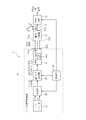
- FIG. 1 shows a ⁇ modulation system according to an embodiment.
- the system 1 includes a digital signal processing unit (digital signal processing device) 21 including a ⁇ modulator 25, a power combiner 51, and an analog filter 32.
- digital signal processing unit 21 including a ⁇ modulator 25, a power combiner 51, and an analog filter 32.
- the digital signal processing unit 21 outputs a band transmission type modulation signal, for example, a digital signal (multi-bit signal) representing an RF (Radio Frequency) signal.
- a band transmission type modulation signal for example, a digital signal (multi-bit signal) representing an RF (Radio Frequency) signal.
- the RF signal is a signal to be radiated to the space as a radio wave, for example, an RF signal for mobile communication and an RF signal for broadcasting services such as television / radio.
- a multi-bit signal (a 2-bit signal in the present embodiment) output from the digital signal processing unit 21 is given to the power combiner 51.
- the power combiner 51 combines the power of each of the plurality of bits to generate a combined signal.
- the synthesized signal is given to an analog filter (bandpass filter or lowpass filter) 32.
- the synthesized signal includes quantization noise outside the signal band of the RF signal, and the quantization noise (noise component) outside the signal band is removed by the analog filter 32.
- the multi-bit signal output from the digital signal processing unit 21 passes through the power combiner 51 and the analog filter 32 to become an analog RF signal. In this way, the synthesized signal represents an analog RF signal, although it contains a noise component outside the signal band.
- the analog filter 32 is a band-pass filter or a low-pass filter is appropriately determined depending on the frequency of the RF signal. As shown in FIG. 1, when the ⁇ modulator 25 is a bandpass type ⁇ modulator, a bandpass filter is used as the analog filter 32, and when it is a lowpass type ⁇ modulator, an analog signal is used. A low-pass filter is used as the filter 32.
- the digital signal processing unit 21 can be regarded as an RF signal transmitter that outputs a multi-bit signal as an RF signal.
- the device having the power combiner 51 and the analog filter 32 is considered as a receiver of the RF signal.
- the entire system 1 may be regarded as a transmitter that transmits an RF signal.
- the digital signal processing unit 21 includes a baseband unit 23 that outputs a baseband signal (IQ signal) that is information transmitted by an RF signal, a processing unit 24 that performs processing such as digital quadrature modulation, a ⁇ modulator 25, The multi-bit output unit 41 and the control unit 35 are provided.
- a baseband unit 23 that outputs a baseband signal (IQ signal) that is information transmitted by an RF signal
- a processing unit 24 that performs processing such as digital quadrature modulation
- a ⁇ modulator 25 The multi-bit output unit 41 and the control unit 35 are provided.
- the baseband unit 23 outputs IQ baseband signals (I signal and Q signal) as digital data.
- the processing unit 24 performs processing such as digital quadrature modulation on the IQ baseband signal. Therefore, the processing unit 24 outputs a signal in a digital signal format expressed by multi-bit digital data (discrete values).
- the modulation in the processing unit 24 is not limited to quadrature modulation, and may be modulation of another method for generating a modulated wave.
- the processing unit 24 performs various digital signal processing such as DPD (Digital Pre-distortion), CFR (Crest Factor Reduction), DUC (Digital Up Conversion) in addition to quadrature modulation.
- the processing unit 24 outputs an RF signal generated by various digital signal processing as described above.
- the digital RF signal output from the processing unit 24 is given to the ⁇ modulator 25.
- the ⁇ modulator 25 of the present embodiment is configured as a bandpass type ⁇ modulator.
- the ⁇ modulator 25 may be a low-pass type, but a band-pass type is advantageous when a high-frequency RF signal is handled.
- the control unit 35 has a control function such as frequency control, and controls each unit in the digital signal processing unit 21 and the analog filter 32.
- the ⁇ modulator 25 includes a loop filter 27 and a quantizer 28.
- an input U (RF signal in the present embodiment) U is given to the loop filter 27.
- the output Y of the loop filter 27 is given to the quantizer 28.
- the output (quantized signal) V of the quantizer 28 is given as another input to the loop filter 27.
- the quantizer 28 When the input signal of the ⁇ modulator 25 takes a positive value and a negative value like an RF signal, the quantizer 28 needs to be able to quantize the positive value and the negative value.
- the quantizer 28 In digital processing, when expressing positive and negative numbers in binary, the most significant bit is the sign bit, indicating positive / negative (0 is positive and 1 is negative), and the absolute number of the number you want to express with the remaining bits Generally, the value is shown in two's complement.
- the characteristics of the ⁇ modulator 25 can be expressed by a signal transfer function (STF) and a noise transfer function (NTF; Noise Transfer Function). That is, when the input of the ⁇ modulator 25 is U, the output of the ⁇ modulator 25 is V, and the quantization noise is E, the characteristics of the ⁇ modulator 25 are expressed in the z region as follows. is there.
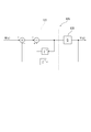
- FIG. 3 shows a block diagram of the linear z-domain model of the first-order low-pass ⁇ modulator 125.
- Reference numeral 127 represents a loop filter portion, and reference numeral 128 represents a quantizer.
- the input to the ⁇ modulator 125 is U (z)
- the output is V (z)
- the quantization noise is E (z)
- the characteristics of the ⁇ modulator 125 are expressed in the z region. It is as follows.
- V (z) U (z) + (1-z ⁇ 1 ) E (z)
- a low pass type ⁇ modulator can be converted into a band pass type ⁇ modulator by performing the following conversion on the low pass type ⁇ modulator.
- an n-order low-pass ⁇ modulator (n is an integer of 1 or more) can be converted to a 2n-order band-pass ⁇ modulator.
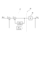
- FIG. 4 shows a second-order band-pass ⁇ modulator 25 obtained by converting the first-order low-pass ⁇ modulator 125 shown in FIG. 3 using the conversion equation (3).
- the conversion to the band-pass type ⁇ modulator can be applied to other high-order low-pass type ⁇ modulators (for example, the CIFB structure, the CRFF structure, the CIFF structure, etc. described in Non-Patent Document 1).
- the ⁇ modulator 25 can convert the value of z based on the above-described equation (3). That is, the ⁇ modulator 307 can change the center frequency of the quantization noise stop band. In other words, the quantization noise stop band can be changed.
- the control unit 35 converts z of the ⁇ modulator 25 based on the above equation (3) according to the center frequency of the signal input to the ⁇ modulator 25 (the carrier frequency f 0 described above).
- Bandpass ⁇ modulation can be performed on a signal having an arbitrary frequency. In this manner, by changing cos ⁇ 0 (coefficient a) in the above conversion equation (3) according to the carrier frequency f 0 of the RF signal, it corresponds to an arbitrary frequency f 0 without changing the sampling frequency fs.
- Bandpass ⁇ modulation can be performed.
- cos ⁇ 0 is changed, the coefficient of NTF shown in Expression (1) is changed, but the order of the expression is maintained.
- the bandpass ⁇ modulator 25 is not changed.
- the signal processing load in the case does not change.
- the present embodiment is advantageous because the signal processing load in the band-pass ⁇ modulator 25 does not change even when the carrier frequency f 0 is changed.
- the signal processing load in the band-pass ⁇ modulator 25 depends on the sampling frequency fs determined by the signal bandwidth according to the Nyquist theorem, but the signal bandwidth even when the carrier frequency f 0 is changed. Therefore, it is not necessary to change the sampling frequency fs.
- the ⁇ modulator is a low-pass type, it is necessary to change the sampling frequency fs in order to cope with a change in the carrier frequency f 0 , and in this respect, the band-pass type is advantageous.
- the ⁇ modulator 25 can be used not only as a bandpass type ⁇ modulator that can cope with an arbitrary frequency (f 0 ) but also as a low pass type ⁇ modulator. That is, the ⁇ modulator 25 can be switched between a low pass type and a band pass type.
- control unit 35 can control the processing unit 24 to change the frequency of the RF signal output from the processing unit 24 to an arbitrary frequency and provide it to the ⁇ modulator 25.
- control unit 35 controls the analog filter 32 so that the center frequency of the analog filter 32 is changed so as to pass the changed frequency of the RF signal.
- the multi-bit output unit 41 is for performing predetermined conversion on an n-value (ternary) quantized signal and outputting it from the digital signal processing unit 21 as a multi-bit (2-bit) parallel signal. Since the multi-bit output unit 41 outputs a 2-bit signal in parallel, the first output port 41a from which the first bit is output and the second output port 41b from which the second bit is output. It is equipped with.
- Each output port 41a, 41b outputs a signal whose voltage is High level or Low level.
- a high level signal is indicated by “VH”
- a low level signal is indicated by “VL”.
- the signal output from the first output port 41a is indicated by “VH 1 ” or “VL 1 ”
- the signal is output from the second output port 41b.
- the output signal is indicated by “VH 2 ” or “VL 2 ”.
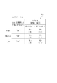
- the multi-bit output unit 41 includes a look-up table 41c for converting an n-valued quantized signal into a multi-bit (2-bit) parallel signal.
- the multi-bit output unit 41 can easily convert an n-valued quantized signal into a multi-bit signal by referring to the lookup table 41c.
- the look-up table 41 c includes a ⁇ modulator output (n-value quantized signal) input to the multi-bit output unit 41 and signals output from the first and second output ports 41 a and 41 b. And holding a combination.
- the output (multi-bit signal) of the multi-bit output unit 41 has n signal levels corresponding to the n-valued quantized signal output from the quantizer 28 when the output is combined by the power combiner 51.
- the power combiner 51 performs power combining on the multi-bit signal output from the multi-bit output unit 41 to generate a combined signal having n signal levels.
- the power combiner 51 includes a first input port 51a and a second input port 51b to which a 2-bit signal output from the multi-bit output unit 41 is input, and an output port 51c that outputs a combined signal.
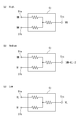
- FIG. 6 shows a first example of the power combiner 51.
- the power combiner 51 of FIG. 6 is configured as a Y-type power combiner, and three resistors 52a, 52b, and 52c are connected in a Y-type.
- the power combiner 51 in FIG. 6 is configured to perform impedance matching with a load (the analog filter 32 in FIG. 1) connected to the output port 51c of the power combiner 51.
- a load the analog filter 32 in FIG. 1
- the impedance of the first input port 51a and the second input port 51b is also a Z 0
- each of the resistors 52a, 52 b, 52c are impedance , Z 0/3 may be set.
- a hybrid combiner may be used as the power combiner 51 instead of the power combiner 51 of FIG.
- the ports can be isolated and the voltage can be set completely independently.
- resistors 52a and 52b are connected to the input ports 51a and 51b, respectively.
- impedance matching can be achieved by setting the impedance of each of the resistors 52a, 52b and 52c to ⁇ (m ⁇ 1) / (m + 1) ⁇ ⁇ Z 0. .
- FIG. 7 shows a second example of the power combiner 51.
- the power combiner 51 of FIG. 6 is configured as a ⁇ -type power combiner, and three resistors 52a, 52b, and 52c are connected in a Y shape.
- the power combiner 51 in FIG. 7 is also configured to match impedance with the load (the analog filter 32 in FIG. 1) connected to the output port 51c of the power combiner 51.
- the characteristic impedance of which is connected to the output port 51c load and Z 0 the impedance of the first input port 51a and the second input port 51b is also a Z 0, each of the resistors 53a, 53b, the impedance of 53c is , Z 0 may be set.
- an analog circuit such as the power combiner 51 needs to be impedance matched. Therefore, it is preferable that impedance matching is taken so as not to adversely affect the RF signal output from the analog filter 32.
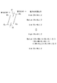
- FIG. 8 shows the signal level of the combined signal (analog signal) output from the output port 51 c of the power combiner 51.
- the Y-type power combiner 51 shown in FIG. 6 is shown for easy understanding, but a similar combined signal can also be obtained by the ⁇ -type power combiner 51 shown in FIG.
- the synthesized signal has n signal levels (High, Medium, Low), like the quantized signal.
- VH +1 [V]
- VH +1 [V]
- VL ⁇ 1 [V]
- the output port 51c outputs (VH + VL) / 2, that is, a signal level (center signal level) of Medium (0 [V]).
- VL (+1 [V]) when VL (+1 [V]) is input to the first input port 51a and VL (-1 [V]) is input to the second input port 51b, power synthesis is performed.
- the output port 51c outputs a signal level (minimum signal level) of VL, that is, Low ( ⁇ 1 [V]).
- the power combiner 51 functions like a digital-analog converter (DAC).
- DAC digital-analog converter
- the medium signal shown in FIG. 8B should ideally have a signal level of zero, which is the median value of the high signal and the low signal. However, in reality, a Medium signal may not be strictly a median of High and Low.
- the combined signal output from the power combiner 51 has a high signal level (VH 1 + VH 2 ) / 2, and a low signal signal.
- the level becomes (VL 1 + VL 2 ) / 2. That is, the signal level of the High signal becomes an average signal level (VH 1 + VH 2 ) / 2 in the bit pattern (VH 1 , VH 2 ) for generating the High signal, and the signal level of the Low signal generates the Low signal. Therefore, the average signal level (VL 1 + VL 2 ) / 2 in the bit pattern (VL 1 , VL 2 ) is set.
- the median value of the High signal and the Low signal is ⁇ (VH 1 + VH 2 ) / 2 + (VL 1 + VL 2 ) / 2 ⁇ / 2.
- the medium signal is (VH 1 + VL 2 ) / 2
- the median value of the high signal and the low signal does not exactly match. Such a shift in the median value becomes a noise component in the RF signal, and becomes a factor that degrades the signal characteristics of the RF signal.
- FIG. 10 shows a lookup table 41c improved to solve such a problem.
- the lookup table 41c in FIG. 10 includes a first table and a second table.
- the first table is for generating a bit pattern similar to the lookup table 41c of FIG.
- the second table is for generating a bit pattern different from the bit pattern in the first table for the Medium signal.
- VH 1 (+1) is output from the first output port 41a when the n-value (ternary) quantized signal is Medium (0) as in the lookup table 41c of FIG.
- VL 2 ( ⁇ 1) is output from the second output port 41b.
- this bit pattern (+1, ⁇ 1) is referred to as a “first bit pattern”.
- the signal level of Medium in the combined signal output from the power combiner 51 is (VH 1 + VL 2 ) / 2.
- VL 1 ( ⁇ 1) is output from the first output port 41a
- VH 2 (+1) is output from the second output port 41b. Is output.
- this bit pattern is referred to as a “second bit pattern”.
- the signal level of Medium in the combined signal output from the power combiner 51 is (VL 1 + VH 2 ) / 2.
- the first bit pattern and the second bit pattern are bit patterns that generate a combined signal of the same signal level by power combining by the power combiner 51. .
- the multi-bit output unit 41 outputs a 2-bit signal with reference to the first table and the second table alternately for the medium (0) quantized signal. Therefore, for the medium (0) quantized signal, the first bit pattern and the second bit pattern are alternately output from the multi-bit output unit 41. Therefore, both bit patterns occur at the same frequency.
- the power combiner 51 has two types of signals, ie, a signal level of (VH 1 + VL 2 ) / 2 and a signal level of (VL 1 + VH 2 ) / 2 for the medium signal level. Are alternately output.
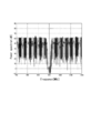
- FIG. 11 shows a voltage waveform when only a signal having a signal level of Medium (0) is continuously output from the power combiner 51.
- two types of signals that is, a signal having a signal level of (VH 1 + VL 2 ) / 2 and a signal having a signal level of (VL 1 + VH 2 ) / 2 are output alternately.
- the medium signal coincides with the median value of the high signal and the low signal when the time average is taken, and the noise component in the RF signal can be reduced.
Landscapes
- Engineering & Computer Science (AREA)
- Physics & Mathematics (AREA)
- Spectroscopy & Molecular Physics (AREA)
- Computer Networks & Wireless Communication (AREA)
- Signal Processing (AREA)
- Theoretical Computer Science (AREA)
- Compression, Expansion, Code Conversion, And Decoders (AREA)
Applications Claiming Priority (2)
| Application Number | Priority Date | Filing Date | Title |
|---|---|---|---|
| JP2012127616A JP5935519B2 (ja) | 2012-06-05 | 2012-06-05 | Δς変調システム |
| JP2012-127616 | 2012-06-05 |
Publications (1)
| Publication Number | Publication Date |
|---|---|
| WO2013183528A1 true WO2013183528A1 (fr) | 2013-12-12 |
Family
ID=49711920
Family Applications (1)
| Application Number | Title | Priority Date | Filing Date |
|---|---|---|---|
| PCT/JP2013/064989 Ceased WO2013183528A1 (fr) | 2012-06-05 | 2013-05-30 | Système de modulation delta-sigma et dispositif de traitement de signal numérique |
Country Status (2)
| Country | Link |
|---|---|
| JP (1) | JP5935519B2 (fr) |
| WO (1) | WO2013183528A1 (fr) |
Families Citing this family (2)
| Publication number | Priority date | Publication date | Assignee | Title |
|---|---|---|---|---|
| KR101551090B1 (ko) | 2014-05-13 | 2015-09-08 | 인하대학교 산학협력단 | 델타 시그마 변조를 이용한 고화질 멀티미디어 인터페이스 표준의 디스플레이 포트 오디오 타임스탬프 변환기 및 그 방법 |
| US10998868B2 (en) | 2017-08-04 | 2021-05-04 | Nec Corporation | RF signal generation device and RF signal generation method |
Citations (5)
| Publication number | Priority date | Publication date | Assignee | Title |
|---|---|---|---|---|
| JPH03117034A (ja) * | 1989-09-28 | 1991-05-17 | Nec Corp | オーバーサンプリング型アナログ・ディジタル変換器 |
| JP2005117431A (ja) * | 2003-10-08 | 2005-04-28 | Nec Electronics Corp | アナログ信号出力回路及び該アナログ信号出力回路を用いたマルチレベルδς変調器 |
| JP2009065420A (ja) * | 2007-09-06 | 2009-03-26 | Renesas Technology Corp | 半導体集積回路装置 |
| JP2009522874A (ja) * | 2005-12-28 | 2009-06-11 | アナログ デバイスズ インコーポレイテッド | デジタル/アナログ変換器およびローパスフィルタに連続時間ステージとスイッチトキャパシタステージとを併用するアーキテクチャ |
| WO2013051641A1 (fr) * | 2011-10-04 | 2013-04-11 | 住友電気工業株式会社 | Procédé de conception destiné à un modulateur δς passe-bande, modulateur δς passe-bande, dispositif comportant un modulateur δς passe-bande, et procédé utilisant une modulation δς passe-bande |
-
2012
- 2012-06-05 JP JP2012127616A patent/JP5935519B2/ja not_active Expired - Fee Related
-
2013
- 2013-05-30 WO PCT/JP2013/064989 patent/WO2013183528A1/fr not_active Ceased
Patent Citations (5)
| Publication number | Priority date | Publication date | Assignee | Title |
|---|---|---|---|---|
| JPH03117034A (ja) * | 1989-09-28 | 1991-05-17 | Nec Corp | オーバーサンプリング型アナログ・ディジタル変換器 |
| JP2005117431A (ja) * | 2003-10-08 | 2005-04-28 | Nec Electronics Corp | アナログ信号出力回路及び該アナログ信号出力回路を用いたマルチレベルδς変調器 |
| JP2009522874A (ja) * | 2005-12-28 | 2009-06-11 | アナログ デバイスズ インコーポレイテッド | デジタル/アナログ変換器およびローパスフィルタに連続時間ステージとスイッチトキャパシタステージとを併用するアーキテクチャ |
| JP2009065420A (ja) * | 2007-09-06 | 2009-03-26 | Renesas Technology Corp | 半導体集積回路装置 |
| WO2013051641A1 (fr) * | 2011-10-04 | 2013-04-11 | 住友電気工業株式会社 | Procédé de conception destiné à un modulateur δς passe-bande, modulateur δς passe-bande, dispositif comportant un modulateur δς passe-bande, et procédé utilisant une modulation δς passe-bande |
Also Published As
| Publication number | Publication date |
|---|---|
| JP5935519B2 (ja) | 2016-06-15 |
| JP2013254994A (ja) | 2013-12-19 |
Similar Documents
| Publication | Publication Date | Title |
|---|---|---|
| US7787563B2 (en) | Transmitter for wireless applications incorporation spectral emission shaping sigma delta modulator | |
| US8755447B2 (en) | Wireless audio equipment using a quadrature modulation system | |
| Li et al. | A 21-GS/s single-bit second-order delta–sigma modulator for FPGAs | |
| US8165549B2 (en) | Method for notch filtering a digital signal, and corresponding electronic device | |
| EP3807997B1 (fr) | Émetteur radiofréquence (rf) et procédé de transmission rf | |
| US9071303B2 (en) | Level de-multiplexed delta sigma modulator based transmitter | |
| US9025700B2 (en) | Digital polar modulator for a switch mode RF power amplifier | |
| JP2013255003A (ja) | Δς変調システム及びデジタル信号処理装置 | |
| WO2013183550A1 (fr) | Dispositif de conversion de signal et émetteur | |
| WO2014192574A1 (fr) | Circuit de transmission | |
| JP5935519B2 (ja) | Δς変調システム | |
| US9077391B2 (en) | Transmitter front-end device for generating output signals on basis of polyphase modulation | |
| US20110007836A1 (en) | Sample rate conversion in delta-sigma modulators | |
| Ralph et al. | Using high pass sigma-delta modulation for Class-S power amplifiers | |
| CN108900202B (zh) | 一种并行的频点灵活可调的∑-δ调制器及其工作方法 | |
| JP6064485B2 (ja) | 信号処理装置及び無線機 | |
| JP5418709B2 (ja) | 信号変換装置及び送信機 | |
| US9264063B2 (en) | Method for designing band pass delta-sigma modulator, band pass delta-sigma modulator, signal processing device, and radio transceiver | |
| CN106817138A (zh) | 一种射频发射机及其信号产生方法 | |
| KR20110070675A (ko) | 디지털 rf 컨버터 및 이를 포함하는 디지털 rf 변조기와 송신기 | |
| JP2014014066A (ja) | 信号変換装置、信号出力装置、及び送信機 | |
| Pereira | Architectures for Beyond 5G All-Digital RF Transmitters | |
| TW201543817A (zh) | 用於射頻通訊的脈衝序列片段的信號調變 | |
| WO2013183534A1 (fr) | Émetteur sans fil et dispositif de traitement de signal | |
| Venkataraman | A practical design methodology for an all-digital transmitter architecture via binary sequence search and a look-up table approach to modulation |
Legal Events
| Date | Code | Title | Description |
|---|---|---|---|
| 121 | Ep: the epo has been informed by wipo that ep was designated in this application |
Ref document number: 13799781 Country of ref document: EP Kind code of ref document: A1 |
|
| NENP | Non-entry into the national phase |
Ref country code: DE |
|
| 122 | Ep: pct application non-entry in european phase |
Ref document number: 13799781 Country of ref document: EP Kind code of ref document: A1 |