WO2013187119A1 - 電界発光素子およびその電界発光素子を用いた照明装置 - Google Patents
電界発光素子およびその電界発光素子を用いた照明装置 Download PDFInfo
- Publication number
- WO2013187119A1 WO2013187119A1 PCT/JP2013/061240 JP2013061240W WO2013187119A1 WO 2013187119 A1 WO2013187119 A1 WO 2013187119A1 JP 2013061240 W JP2013061240 W JP 2013061240W WO 2013187119 A1 WO2013187119 A1 WO 2013187119A1
- Authority
- WO
- WIPO (PCT)
- Prior art keywords
- transparent electrode
- transparent
- light emitting
- emitting layer
- electroluminescent element
- Prior art date
- Legal status (The legal status is an assumption and is not a legal conclusion. Google has not performed a legal analysis and makes no representation as to the accuracy of the status listed.)
- Ceased
Links
Images









Classifications
-
- H—ELECTRICITY
- H10—SEMICONDUCTOR DEVICES; ELECTRIC SOLID-STATE DEVICES NOT OTHERWISE PROVIDED FOR
- H10K—ORGANIC ELECTRIC SOLID-STATE DEVICES
- H10K59/00—Integrated devices, or assemblies of multiple devices, comprising at least one organic light-emitting element covered by group H10K50/00
- H10K59/80—Constructional details
- H10K59/805—Electrodes
- H10K59/8052—Cathodes
- H10K59/80524—Transparent cathodes, e.g. comprising thin metal layers
-
- H—ELECTRICITY
- H10—SEMICONDUCTOR DEVICES; ELECTRIC SOLID-STATE DEVICES NOT OTHERWISE PROVIDED FOR
- H10K—ORGANIC ELECTRIC SOLID-STATE DEVICES
- H10K50/00—Organic light-emitting devices
- H10K50/80—Constructional details
- H10K50/805—Electrodes
- H10K50/81—Anodes
- H10K50/816—Multilayers, e.g. transparent multilayers
-
- H—ELECTRICITY
- H10—SEMICONDUCTOR DEVICES; ELECTRIC SOLID-STATE DEVICES NOT OTHERWISE PROVIDED FOR
- H10K—ORGANIC ELECTRIC SOLID-STATE DEVICES
- H10K50/00—Organic light-emitting devices
- H10K50/80—Constructional details
- H10K50/805—Electrodes
- H10K50/82—Cathodes
- H10K50/828—Transparent cathodes, e.g. comprising thin metal layers
-
- H—ELECTRICITY
- H10—SEMICONDUCTOR DEVICES; ELECTRIC SOLID-STATE DEVICES NOT OTHERWISE PROVIDED FOR
- H10K—ORGANIC ELECTRIC SOLID-STATE DEVICES
- H10K50/00—Organic light-emitting devices
- H10K50/80—Constructional details
- H10K50/85—Arrangements for extracting light from the devices
-
- H—ELECTRICITY
- H10—SEMICONDUCTOR DEVICES; ELECTRIC SOLID-STATE DEVICES NOT OTHERWISE PROVIDED FOR
- H10K—ORGANIC ELECTRIC SOLID-STATE DEVICES
- H10K50/00—Organic light-emitting devices
- H10K50/80—Constructional details
- H10K50/85—Arrangements for extracting light from the devices
- H10K50/858—Arrangements for extracting light from the devices comprising refractive means, e.g. lenses
-
- H—ELECTRICITY
- H10—SEMICONDUCTOR DEVICES; ELECTRIC SOLID-STATE DEVICES NOT OTHERWISE PROVIDED FOR
- H10K—ORGANIC ELECTRIC SOLID-STATE DEVICES
- H10K59/00—Integrated devices, or assemblies of multiple devices, comprising at least one organic light-emitting element covered by group H10K50/00
- H10K59/80—Constructional details
- H10K59/805—Electrodes
- H10K59/8051—Anodes
- H10K59/80517—Multilayers, e.g. transparent multilayers
-
- H—ELECTRICITY
- H10—SEMICONDUCTOR DEVICES; ELECTRIC SOLID-STATE DEVICES NOT OTHERWISE PROVIDED FOR
- H10K—ORGANIC ELECTRIC SOLID-STATE DEVICES
- H10K59/00—Integrated devices, or assemblies of multiple devices, comprising at least one organic light-emitting element covered by group H10K50/00
- H10K59/80—Constructional details
- H10K59/875—Arrangements for extracting light from the devices
- H10K59/879—Arrangements for extracting light from the devices comprising refractive means, e.g. lenses
-
- H—ELECTRICITY
- H10—SEMICONDUCTOR DEVICES; ELECTRIC SOLID-STATE DEVICES NOT OTHERWISE PROVIDED FOR
- H10K—ORGANIC ELECTRIC SOLID-STATE DEVICES
- H10K2102/00—Constructional details relating to the organic devices covered by this subclass
- H10K2102/301—Details of OLEDs
- H10K2102/302—Details of OLEDs of OLED structures
- H10K2102/3023—Direction of light emission
- H10K2102/3031—Two-side emission, e.g. transparent OLEDs [TOLED]
-
- H—ELECTRICITY
- H10—SEMICONDUCTOR DEVICES; ELECTRIC SOLID-STATE DEVICES NOT OTHERWISE PROVIDED FOR
- H10K—ORGANIC ELECTRIC SOLID-STATE DEVICES
- H10K50/00—Organic light-emitting devices
- H10K50/10—OLEDs or polymer light-emitting diodes [PLED]
- H10K50/11—OLEDs or polymer light-emitting diodes [PLED] characterised by the electroluminescent [EL] layers
-
- H—ELECTRICITY
- H10—SEMICONDUCTOR DEVICES; ELECTRIC SOLID-STATE DEVICES NOT OTHERWISE PROVIDED FOR
- H10K—ORGANIC ELECTRIC SOLID-STATE DEVICES
- H10K50/00—Organic light-emitting devices
- H10K50/10—OLEDs or polymer light-emitting diodes [PLED]
- H10K50/14—Carrier transporting layers
- H10K50/15—Hole transporting layers
-
- H—ELECTRICITY
- H10—SEMICONDUCTOR DEVICES; ELECTRIC SOLID-STATE DEVICES NOT OTHERWISE PROVIDED FOR
- H10K—ORGANIC ELECTRIC SOLID-STATE DEVICES
- H10K50/00—Organic light-emitting devices
- H10K50/10—OLEDs or polymer light-emitting diodes [PLED]
- H10K50/14—Carrier transporting layers
- H10K50/16—Electron transporting layers
-
- H—ELECTRICITY
- H10—SEMICONDUCTOR DEVICES; ELECTRIC SOLID-STATE DEVICES NOT OTHERWISE PROVIDED FOR
- H10K—ORGANIC ELECTRIC SOLID-STATE DEVICES
- H10K50/00—Organic light-emitting devices
- H10K50/80—Constructional details
- H10K50/85—Arrangements for extracting light from the devices
- H10K50/856—Arrangements for extracting light from the devices comprising reflective means
-
- H—ELECTRICITY
- H10—SEMICONDUCTOR DEVICES; ELECTRIC SOLID-STATE DEVICES NOT OTHERWISE PROVIDED FOR
- H10K—ORGANIC ELECTRIC SOLID-STATE DEVICES
- H10K59/00—Integrated devices, or assemblies of multiple devices, comprising at least one organic light-emitting element covered by group H10K50/00
- H10K59/80—Constructional details
- H10K59/875—Arrangements for extracting light from the devices
- H10K59/878—Arrangements for extracting light from the devices comprising reflective means
Definitions
- the present invention relates to an electroluminescent element and an illumination device using the electroluminescent element.
- electroluminescent elements such as light emitting diodes (LEDs) and organic EL (Electro-Luminescence) have attracted attention.
- the electroluminescent element is composed of a light emitting layer sandwiched between a planar cathode and an anode.
- the anode is often a transparent electrode and the cathode is a metal reflective electrode.
- one of them is constituted by a metal reflective electrode, light is extracted from the transparent anode side and used as a single-sided light emitting device.
- JP-A-10-294182 Patent Document 1
- JP-A-2012-15122 Patent Document 2
- JP-A-2011-65781 Patent Document 3
- transparent electrodes are used for a cathode and an anode.
- An electroluminescent element used as a transparent surface-emitting light source is disclosed.
- the plasmon absorption loss caused when a metal reflective electrode is used on one side is reduced, and a more efficient electroluminescent element is realized. Is possible.
- the transparent electroluminescent element is rich in design and suitable for producing an expansion of space.
- an electroluminescent device when used as a surface-emitting light source for illumination, when used as transmissive illumination such as a window, a show window, and a showcase, the emitted light is irradiated only on one side and there is no light scattering. It is important to ensure transparency.
- Patent Documents 1, 2, and 3 there is no description regarding the difference in light emission intensity between the front surface and the back surface of the electroluminescent element, and a method for biasing the light emission intensity between the front surface and the back surface of the light emitting element itself to one side. Is unknown.
- the present invention has been made in view of the above problems, and provides an electroluminescent element capable of biasing light emission to one side of the electroluminescent element while ensuring the transparency of the electroluminescent element, and an electroluminescent element thereof It aims at providing the used illuminating device.
- the reflectance of the interface between the light emitting layer and the first transparent electrode is higher than the reflectance of the interface between the light emitting layer and the second transparent electrode.
- the refractive index of the transparent electrode and the second transparent electrode is selected, and the refractive index of the first transparent member is provided to be lower than the refractive index of the second transparent member.
- an electroluminescent element capable of biasing light emission to one side of the electroluminescent element while ensuring the transparency of the electroluminescent element, and an illumination device using the electroluminescent element. make it possible.
- FIG. 3 is a cross-sectional view corresponding to a cross section taken along line II in FIG. 2 and showing a minimum configuration for realizing an electroluminescent element. It is a top view of an electroluminescent element. It is a schematic diagram for demonstrating the light emission intensity difference by the difference in the reflectance of the light in the interface of a light emitting layer and each transparent electrode. It is sectional drawing of the electroluminescent element in Example 1 based on Embodiment 1. FIG. It is a schematic diagram for demonstrating the light emission intensity difference by the difference in the reflectance of the light in the interface of the light emitting layer of the electroluminescent element in Example 1 based on Embodiment 1, and each transparent electrode.
- Respective refractive indexes of the first transparent member, the first transparent electrode, the light emitting layer, the second transparent electrode, and the second transparent member of the electroluminescent elements in Examples 5 to 16 based on Embodiment 2 are shown.
- FIG. Respective refractive indexes of the first transparent member, the first transparent electrode, the light emitting layer, the second transparent electrode, and the second transparent member of the electroluminescent elements in Examples 17 to 28 based on the second embodiment are shown.
- Respective refractive indexes of the first transparent member, the first transparent electrode, the light emitting layer, the second transparent electrode, and the second transparent member of the electroluminescent elements in Examples 29 to 36 based on the second embodiment are shown.
- FIG. 37 It is a figure which shows the glass material (10 types) which can be used as a material of a 1st transparent member or a 2nd transparent member. It is a figure which shows the cross-section of the electroluminescent element in Example 37 based on Embodiment 2.
- FIG. 38 It is a figure which shows the cross-section of the electroluminescent element in Example 38 based on Embodiment 2.
- FIG. 39 It is a figure which shows the cross-section of the electroluminescent element in Example 39 based on Embodiment 2.
- FIG. 40 It is a figure which shows the cross-section of the electroluminescent element in Example 40 based on Embodiment 2.
- FIG. 41 shows the cross-section of the electroluminescent element in Example 41 based on Embodiment 2.
- FIG. 42 It is a figure which shows the cross-section of the electroluminescent element in Example 42 based on Embodiment 2.
- FIG. It is a figure which shows the cross-section of the electroluminescent element in Example 43 based on Embodiment 2.
- FIG. It is a figure which shows the cross-section of the electroluminescent element in Example 44 based on Embodiment 2.
- FIG. It is a figure which shows the cross-section of the electroluminescent element in Example 45 based on Embodiment 2.
- FIG. It is a figure which shows the cross-section of the electroluminescent element in Example 46 based on Embodiment 2.
- FIG. It is a figure which shows schematic structure of the illuminating device in Embodiment 3.
- FIG. It is a figure which shows the internal structure of the illuminating device in Embodiment 3.
- FIG. 1 is a cross-sectional view of the electroluminescent element 1, and corresponds to a cross section taken along line II in FIG.
- FIG. 2 is a plan view of the electroluminescent element 1.
- the electroluminescent element 1 includes a first transparent electrode 11, a second transparent electrode 12, and a light emitting layer 10 sandwiched between the first transparent electrode 11 and the second transparent electrode 12.
- a voltage between the first transparent electrode 11 and the second transparent electrode 12 electrons are accelerated and injected into the light emitting layer 10, and the kinetic energy of the electrons is converted into photons in the light emitting layer 10.
- Light is extracted to the first transparent electrode 11 and the second transparent electrode 12.
- first transparent electrode 11 and the second transparent electrode 12 are used for the first transparent electrode 11 and the second transparent electrode 12 in order to facilitate electron injection.
- a thin film metal electrode Al, Au, Cu, etc.
- a transparent oxide semiconductor electrode ITO (indium) having a work function suitable for hole injection on the anode side Oxide and tin oxide
- IZO mixed oxide and zinc oxide
- a thin film metal electrode is excellent in electron transport properties, but has a low optical transmittance. Therefore, when used as a transparent electrode, a film thickness of several nm to several tens of nm is suitable for increasing the transmittance.
- the transparent oxide semiconductor electrode is characterized by a large sheet resistance per thickness and a high transmittance as compared with a thin film metal electrode. Therefore, when a transparent oxide semiconductor is used as an electrode, the transparent oxide semiconductor electrode has a thickness of 10 nm to 200 nm in order to reduce the sheet resistance. The film thickness is suitable.
- the electron injection performance is lowered, the drive voltage is increased, and the light emission efficiency is lowered, which is not desirable. Therefore, it is desirable to use different materials for the first transparent electrode 11 and the second transparent electrode 12 so that one transparent electrode has better electron injection property and the other transparent electrode has better hole injection property.
- the electrode material is different between the first transparent electrode 11 and the second transparent electrode 12, it is necessary to consider the reflectance of light at the interface between the light emitting layer 10 and each transparent electrode.
- the reflectance is different between the first transparent electrode 11 side and the second transparent electrode 12 side.
- FIG. 3 is a schematic diagram for explaining a difference in light emission intensity due to a difference in light reflectance at the interface between the light emitting layer 10 and each transparent electrode. For example, as shown in FIG. 3, consider a case where the reflectance on the first transparent electrode 11 side is high and the reflectance on the second transparent electrode 12 side is low.
- the intensity of light extracted outside the first transparent electrode 11 and light extracted outside the second transparent electrode 12 is It is desirable to bias to one electrode side.
- FIG. 3 in the configuration in which the reflectance of the light emitting layer 10 and the first transparent electrode 11 is higher than the reflectance of the light emitting layer 10 and the second transparent electrode 12, from the relationship of the electrode reflectance. It is more efficient to bias the emission intensity only to the second transparent electrode 12 side.
- the transmittance of the first transparent electrode 11 needs to be higher than a certain level (for example, 60%), and the light emission on the first transparent electrode 11 side inevitably remains. there were.
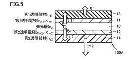
- FIG. 4 is a cross-sectional view of the electroluminescent element 100A in this example, and FIG. 5 shows the difference in emission intensity due to the difference in light reflectance at the interface between the light emitting layer of the electroluminescent element 100A and each transparent electrode in this example. It is a schematic diagram for demonstrating.
- the cross section in FIG. 4 corresponds to the cross section taken along the line II in FIG.
- the electroluminescent element 100 ⁇ / b> A in this example includes a first transparent electrode 11, a second transparent electrode 12, and a light emitting layer 10 sandwiched between the first transparent electrode 11 and the second transparent electrode 12.
- a first transparent member 13 is provided on the surface of the first transparent electrode 11 opposite to the light emitting layer 10.
- a second transparent member 14 is provided on the surface of the second transparent electrode 12 opposite to the light emitting layer 10.
- the first transparent When viewed from the light emitting layer 10, the first transparent so that the reflectance at the interface between the light emitting layer 10 and the first transparent electrode 11 is higher than the reflectance at the interface between the light emitting layer 10 and the second transparent electrode 12.
- the refractive indexes of the electrode 11 and the second transparent electrode 12 are selected.
- the first transparent member 13 is provided so that the refractive index thereof is lower than the refractive index of the second transparent member 14.
- the film thickness of the basic electroluminescent element (light emitting layer 10 + first transparent electrode 11 + second transparent electrode 12) sandwiched between the second transparent electrode 12 and the first transparent electrode 11 is the electric field strength with respect to the applied voltage. In order to prevent an increase in voltage and voltage drop due to internal resistance, it is often in the range of about 100 nm to 500 nm.
- ⁇ 1 and ⁇ 2 can be expressed by the following (Equation 1) using an approximately common proportionality coefficient.
- G is a constant depending on the electric field distribution of the emitted light
- n d1 is the refractive index of the first transparent member 13
- n d2 is the refractive index of the second transparent member 14.
- P 1 is the probability that the generated photon will go to the first transparent member 13
- P 2 is the probability that the generated photon will go to the second transparent member 14.
- the thickness of the transparent member is set so that the wavelength of light in the transparent member (when the vacuum wavelength is ⁇ 0 , the wavelength of the first transparent member 13 is ⁇ 0 / n d1 , second
- the wavelength of the transparent member 14 is desirably larger than ⁇ 0 / n d2 ).
- first transparent member 13 and the second transparent member 14 have a thickness of about several hundred ⁇ m in order to increase the mechanical strength of the light emitting element. At this time, the behavior of light in the transparent member is approximated by geometric optics.
- the angular distribution of light moved from the light emitting layer to the transparent member can be approximated by Lambert (cos ⁇ orientation).
- the ratio ⁇ 1 of light emitted from the first transparent member 13 having a refractive index n d1 to the air having a refractive index 1 and the ratio ⁇ of light emitted from the second transparent member 14 having a refractive index n d2 to the air having a refractive index 1 2 can be expressed as shown below (Formula 3).
- Equation 3 is obtained by integrating the light rays on the assumption that the orientation is Lambert and that all the light within the total reflection angle goes out to the air.
- Equation 1 a ratio of photon number M 2 of (Equation 3) and the photon number M 1 of light exiting More of the first transparent member 13 side air exiting the air in the second transparent member 14 side following (Equation 4) Will be represented.
- This photon number M 1 leaving the first transparent member 13 side is proportional to the refractive index n d1 of the first transparent member 13, the number of photons M 2 exiting the second transparent member 14 side, the second transparent member 14 It is proportional to the refractive index n d2 of.
- the reflectance of the first transparent electrode 11 viewed from the light emitting layer 10 is the reflectance of the second transparent electrode 12 viewed from the light emitting layer 10.
- the reflectance of the second transparent electrode 12 viewed from the light emitting layer 10. Think of a higher state.
- a material having a refractive index of 1.1 is used as the first transparent member 13 and a material having a refractive index of 1.9 is provided as the refractive index of the second transparent member 14 outside the first transparent electrode 11. think of.
- a glass material As the material, a glass material, a resin material, a semiconductor oxide, a metal oxide, and the like can be considered. However, any transparent material such as rubber, liquid, gas, or gel can be used as long as it is a transparent material.
- An example of a medium having a high refractive index in visible light is TiO 2 (refractive index 2.5), and an example of a material having a low refractive index is a resin medium (refractive index 1.1) in which hollow silica fine particles are dispersed. can give.
- the ratio of the number of photons changes according to (Equation 4). As a result, the ratio between the light L 1 ′ exiting the first transparent member 13 and the light L 2 ′ exiting the second transparent member 14 is on the second transparent member 14 side as shown in the following (Formula 5). It becomes possible to bias strongly.
- the electroluminescent element 100A controls the refractive index of the first transparent member 13 and the second transparent member 14, and thereby the light emitted to the first transparent electrode 11 side.
- the ratio of light emitted to the second transparent electrode 12 side is strongly biased toward the second transparent member 14 side, and the transparency of the electroluminescent element 100A can be maintained.
- the organic EL is not limited to organic EL that emits light and is common to all electroluminescent elements having a light emitting layer sandwiched between transparent electrodes, for example, an inorganic electroluminescent element or an element that emits light in the infrared. Also good.
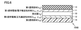
- FIG. 6 shows an organic electroluminescent element 100B as Example 2
- FIG. 7 shows an organic electroluminescent element 100C as Example 3
- FIG. 8 shows an organic electroluminescent element 100D as Example 4.
- 6 to 8 are views showing the cross-sectional structures of the organic electroluminescent elements 100B to 100D.
- the first transparent electrode 11 is a metal thin film with good electron injection property
- the second transparent electrode 12 side is a transparent oxide semiconductor with good hole injection property. It was.
- the first transparent electrode 11 side is a cathode
- the second transparent electrode 12 side is an anode.
- the reflectance of the interface between the light emitting layer 10 and the first transparent electrode 11 viewed from the light emitting layer 10 is higher than the reflectance of the interface between the light emitting layer 10 and the second transparent electrode 12 viewed from the light emitting layer 10.
- the refractive indexes of the first transparent electrode 11 and the second transparent electrode 12 are configured.
- any fluorescent material and phosphorescent material known as organic EL materials can be used. If necessary, a hole transport layer may be provided on the anode side of the light emitting layer 10 or an electron transport layer may be provided on the cathode side of the light emitting layer 10.
- the material of the light-emitting layer 10 is preferably an organic metal complex as a material for an organic EL device from the viewpoint of preferably improving the quantum efficiency of external extraction of the device and prolonging the light emission lifetime.
- the metal involved in complex formation is preferably any one metal belonging to Groups 8 to 10 of the periodic table, Al or Zn, and in particular, the metal is Ir, Pt, Al or Zn. Is preferred.
- the first transparent electrode 11 is an electron transporting material
- the second transparent electrode 12 is a hole transporting material.
- the refractive index of the first transparent electrode 11 is set to be lower than the refractive index of the second transparent electrode 12, so that the electron injection property is obtained by the effect of (Equation 4). Therefore, it is possible to bias the emission intensity toward the second transparent electrode 12 in a state where the transparency is maintained well.
- the complex relative dielectric constant ⁇ c is an optical constant related to interface reflection, and is a physical quantity represented by (Expression 6) using the refractive index n and the extinction coefficient ⁇ .
- Equation 6 P and E are the polarization and electric field, respectively, and ⁇ 0 is the dielectric constant in vacuum. That is, it can be seen that the smaller the refractive index n and the larger the extinction coefficient ⁇ , the smaller the real part of the complex relative dielectric constant ⁇ c.
- n is about 0.1
- the extinction coefficient ⁇ has a large value of 2 to 10 and has a large change rate with respect to the wavelength. Therefore, even if n is the same value, the value of the extinction coefficient ⁇ is greatly different, and there is often a large difference in electron transport performance.
- the refractive index configuration that realizes efficient electron injection has the refractive index of the first transparent electrode 11 as n m1 , the extinction coefficient of the first transparent electrode 11 as ⁇ m1 , and the refractive index of the light emitting layer as ng .
- the refractive index of the second transparent electrode 12 is n m2 and the extinction coefficient of the second transparent electrode 12 is ⁇ m2 , the following (formula 7) is satisfied.
- the reflectance that affects the optical characteristics can be estimated using the Fresnel reflection coefficient of the interface.
- the Fresnel coefficient F 1 at the interface between the light emitting layer 10 and the first transparent electrode 11 and the Fresnel coefficient F 2 at the interface between the light emitting layer 10 and the second transparent electrode 12 are expressed by the following (formula 8).
- the refractive index of the first transparent member 13 is n d1
- the refractive index of the second transparent member 14 is n d2
- the refractive index of the first transparent electrode 11 is n m1
- the refractive index n g of the light-emitting layer 10 is the refractive index of the second transparent electrode 12 and n m @ 2
- FIG. 7 shows a cross-sectional structure of an organic electroluminescent element 100C as Example 3.
- the reflectance of the interface between the light emitting layer 10 and the first transparent electrode 11 viewed from the light emitting layer 10 is the same as that between the light emitting layer 10 and the second transparent electrode 12 viewed from the light emitting layer 10.
- the refractive index of the 1st transparent electrode 11 and the 2nd transparent electrode 12 is comprised so that it may become higher than the reflectance of an interface, and a Fresnel coefficient is not essential.
- Equation 9 is useful in that the constituent conditions of the refractive index of the present embodiment can be calculated by a simple method.
- the relationship between the refractive index nd1 of the first transparent member 13 and the refractive index nd2 of the second transparent member 14 is (Equation 10) below.
- the emission intensity can be biased toward the second transparent electrode 12 in a state where the electron injection property is good and the transparency is maintained.
- Organic electroluminescent element 100D In FIG. 8, the refractive index and film thickness of the organic electroluminescent element 100D as Example 4 and the reflectance at the interface between the light emitting layer and the transparent electrode will be described in detail using specific values.
- an organic material When an organic material is used for the light emitting layer 10, it typically has a refractive index between 1.6 and 1.8 in the visible light region.
- Alq3 film thickness 50 nm
- ⁇ -NPD hole transport layer
- Alq3 is tris (8-quinolinolato) aluminum
- ⁇ -NPD is 4,4′-bis [N- (1-naphthyl) -N-phenylamino] biphenyl.
- the average refractive index of the light emitting layer 10 is 1.8 at a wavelength of 520 nm.
- Examples of materials and refractive indexes used for each member will be described at a wavelength of 520 nm.
- a high refractive index resin film epoxy resin
- a resin film acrylic resin having a refractive index of 1.65 was used.
- a resin substrate having a refractive index of 1.5 is provided as the second transparent member 14, and an ITO thin film having a thickness of 100 nm is provided as the second transparent electrode 12 thereon.
- ⁇ -NPD (50 nm) and Alq3 (50 nm) are sequentially laminated as the light emitting layer 10.
- ⁇ -NPD is laminated as a hole transport layer between the second transparent electrode 12 and Alq3, and the first transparent electrode 11 is provided on Alq3.
- a thin Ag electrode (thickness 20 nm) is formed as the first transparent electrode 11.
- the first transparent member 13 is sealed with a high refractive index resin film (epoxy resin). If necessary, an electrode extraction step is provided in each step to extract the electrode terminal to the outside.
- the respective refractive indexes and extinction coefficients of the first transparent member 13, the first transparent electrode 11, the light emitting layer 10, the second transparent electrode 12, and the second transparent member 14 are used. Is as shown in FIG. This satisfies the conditions of the present embodiment shown in (Equation 9) and (Equation 10).
- the refractive index conditions suitable for electron injection (Formula 7) and (Formula 8) are also satisfied.
- the second transparent electrode is obtained as compared with the case where the transparent member is not used while ensuring the electron injection performance and the transparency of the organic electroluminescent element. 12 and the second transparent member 14 can be secured.
- the transparent electrodes it is important to combine the refractive indexes of the transparent electrodes and the transparent members.
- dielectric materials examples include diamond, calcium fluoride (CaF), silicon nitride (Si 3 N 4 ), and the like.
- a glass material that can be used as a transparent member a commercially available glass material having a refractive index of 1.4 to 1.8 is known.
- the resin material examples include vinyl chloride, acrylic, polyethylene, polypropylene, polystyrene, ABS, nylon, polycarbonate, polyethylene terephthalate, polyvinylidene fluoride, Teflon (registered trademark), polyimide, phenol resin, and a refractive index of 1.4 to There is 1.8.
- Other methods for controlling the refractive index of the transparent member include a method using a photonic crystal provided with a dielectric periodic structure or a plasmonic crystal having a fine metal structure.
- the transparent member may be an inert gas such as nitrogen, a fluid, or a gel.
- a material that can be used as a transparent electrode will be described.
- a metal thin film having good electrical conductivity can be used as the transparent conductive film.
- aluminum (Al) and silver (Ag) are desirable.
- gold (Au) which has an advantage that is not easily oxidized can be considered.
- Another material is copper (Cu), which is characterized by good conductivity.
- Other materials that have good thermal and chemical properties and are not easily oxidized at high temperatures and do not cause chemical reaction with the substrate material include platinum, rhodium, palladium, ruthenium, iridium, and osmium.
- An alloy using a plurality of metal materials may be used.
- MgAg and LiAl are often used as thin film transparent metal electrodes.
- the metal thin film has excellent electron transport performance and is used as an electron transport electrode.
- an electrode using a thin-film metal or a thin-film metal alloy has a feature of high reflectance as viewed from the light emitting layer.
- a material excellent in hole transportability will be described.
- Examples of the material used as the hole transporting electrode include transparent oxide semiconductors (ITO, IZO, ZnO, InGaO 3 ) and the like.
- a transparent oxide semiconductor has a feature that its refractive index is close to that of an organic material and its reflectance as viewed from the light emitting layer is low.
- Conductive resin that can be produced at low cost using a coating method may be used for the transparent electrode.
- a perylene derivative or a fullerene derivative such as PCBM (phenyl C61 butyric acid methyl ester) can be considered.
- the conductive resin material used as the hole transporting electrode is PEDOT (Poly (3,4-ethylenedioxythiophene)) / PSS (Poly (4-styrenesulfonate)), P3HT (Poly (3-hexylthiophene)), P3OT (Poly ( 3-octylthiophene), P3DDT ((Poly (3-dodecylthiophene-2,5-Diyl))), F8T2 (a copolymer of fluorene and bithiophene) and the like.
- PEDOT Poly (3,4-ethylenedioxythiophene)
- PSS Poly (4-styrenesulfonate
- P3HT Poly (3-hexylthiophene)
- P3OT Poly ( 3-octylthiophene)
- P3DDT ((Poly (3-dodecylthiophene-2,5-Diyl))
- F8T2 a
- the reflectance is lower than that of PCBM.
- a metal mesh, metal nanowire, metal nanoparticle or the like may be used in combination.
- the electronic conductivity of the electrode using the metal nanowire is increased, the average refractive index tends to be low, and the reflectance as viewed from the light emitting layer tends to be high.
- the refractive index of the transparent member of the present embodiment is used in order to bias the emission intensity to one side while ensuring transparency while combining two types of transparent electrodes to improve electron injection properties. It is essential to set the conditions.
- FIG. 10 shows Examples 5 to 16 of the electroluminescent element based on the present embodiment.
- the refractive index design of the first transparent member, the first transparent electrode, the light emitting layer, the second transparent electrode, and the second transparent member illustrated in FIG. 10 can be realized using the materials exemplified so far. (Formula 9) and (Formula 10) which are requirements of the form of the above are satisfied.
- FIG. 11 shows Examples 17 to 28 of the electroluminescent element based on the present embodiment.
- the design of the refractive indexes of the first transparent member, the first transparent electrode, the light emitting layer, the second transparent electrode, and the second transparent member shown in FIG. 11 can be realized using the materials exemplified so far. (Formula 9) and (Formula 10) which are requirements of the form of the above are satisfied. Furthermore, the refractive index design shown in FIG. 11 satisfies the condition of refractive index with good electron injection property (Equation 7).
- FIG. 12 shows Examples 29 to 36 of the electroluminescent element based on the present embodiment.
- a hole transporting material is used for the first transparent electrode 11 and an electron transporting material is used for the second transparent electrode 12.
- the refractive index design of the first transparent member, the first transparent electrode, the light emitting layer, the second transparent electrode, and the second transparent member shown in FIG. 12 can be realized using the materials exemplified so far. (Formula 9) and (Formula 10) which are requirements of the form of the above are satisfied.
- the transparent electrode is formed of a resin material.
- a transparent oxide semiconductor such as ITO
- a vacuum process such as a sputtering method is required, but a vacuum process is not required in the case of a coating process.
- the design shown in FIG. 12 has an advantage that the transparent electrode is formed of a resin material, so that a coating process can be applied and the manufacturing cost can be reduced. Since a transparent electrode can be formed by a simpler coating process without using a vacuum process such as sputtering, it is also suitable for mass production.
- FIG. 13 illustrates glass materials (10 types) that can be used as the material of the first transparent member 13 or the second transparent member 14 (glass member manufactured by OHARA). There is a glass material having a visible refractive index of 1.50 to 1.90.
- the transparent electrode is not limited to a single film, and a plurality of films may be combined.
- a structure combined with a transparent conductive film can be considered in order to improve the conductive performance.
- 14 and 15 show the structure of an electroluminescent element in another embodiment.
- a transparent electrode with high electron injection performance such as a metal thin film
- a transparent electrode such as ITO with high hole injection performance is in contact with the anode side of the light emitting layer.
- the total film thickness of the transparent electrodes is preferably equal to or less than the wavelength of the light emitting layer in order to enhance the effect of the present embodiment.
- the refractive index n e of the light-emitting layer as 0 a vacuum wavelength of the emitted light lambda, the wavelength of the light emitting layer is represented by lambda 0 / n e.
- the film thickness of the transparent electrode is desirably 305 nm or less.
- FIG. 14 shows a cross-sectional structure of the electroluminescent element 100E of Example 37.
- the first transparent electrode 11 has a two-layer structure, the transparent electrode 11a using ITO is provided on the first transparent member 13 side, and silver (Ag) is used on the light emitting layer 10 side.
- the transparent electrode 11b was provided.
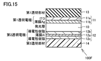
- FIG. 15 shows an electroluminescent element 100F of Example 38.
- the electroluminescent element 100F has a second transparent electrode 12 having a three-layer structure, a transparent electrode 12a using aluminum (Al), and a conductive material sandwiching the transparent electrode 12a.
- Transparent electrodes 12b and 12c using a conductive resin are provided.
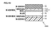
- FIG. 16 shows an electroluminescent element 100G as Example 39.
- a conductive resin is used for the transparent electrode 11a of the electroluminescent element 100E shown in FIG.
- Other configurations are the same as those of the electroluminescent element 100G.
- FIG. 17 shows an electroluminescent element 100H as Example 40.
- a conductive resin is used for the transparent electrode 11a of the electroluminescent element 100F shown in FIG.
- Other configurations are the same as those of the electroluminescent element 100F.
- the conductive resin can be manufactured by a coating process and is suitable for mass production of electroluminescent elements.
- the electron injection property can be improved by assisting the electrode performance.
- 18 and 19 show examples of specific film thickness configurations of the transparent member and the transparent electrode.
- the film thickness of the transparent electrode is equal to or less than the wavelength of the light emitting layer, and the film thickness of the transparent member satisfies the condition that it is equal to or greater than the film thickness of the transparent member.
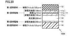
- a resin film having a film thickness of 125 ⁇ m is used for the second transparent member 14.
- a conductive resin having a thickness of 200 nm is used for the second transparent electrode 12.
- the light emitting layer 10 has a thickness of 200 nm.
- the first transparent electrode 11 includes a transparent electrode 11a having a thickness of 100 nm using ITO, a transparent electrode 11b having a thickness of 10 nm using silver (Ag), and a transparent electrode 11c having a thickness of 100 nm using a conductive resin.
- Layer structure For the first transparent member 13, a resin film having a film thickness of 125 ⁇ m is used for the first transparent member 13.
- a resin film having a film thickness of 125 ⁇ m is used for the second transparent member 14.
- a conductive resin having a thickness of 200 nm is used for the second transparent electrode 12.
- the light emitting layer 10 has a thickness of 200 nm.
- the first transparent electrode 11 has a two-layer structure of a transparent electrode 11a having a thickness of 100 nm using ITO and a transparent electrode 11b having a thickness of 10 nm using silver (Ag).
- a resin film having a film thickness of 500 nm is used for the first transparent member 13.
- the second transparent electrode 12 and the second transparent member 14 are also used as compared with the case where the transparent member is not used while ensuring the electron injection performance and the transparency of the organic electroluminescent element. It is possible to ensure light emission that is biased to the side.
- FIG. 20 shows an electroluminescent element 100K as Example 43.
- a conductive resin is used for the transparent electrode 11a of the electroluminescent element 100I shown in FIG.
- Other configurations are the same as those of the electroluminescent element 100I.
- FIG. 21 shows an electroluminescent element 100L as Example 44.
- a conductive resin is used for the transparent electrode 11a of the electroluminescent element 100J shown in FIG.
- Other configurations are the same as those of the electroluminescent element 100J.
- the first transparent member 13 and the transparent electrode 11a use the same conductive resin, they may be composed of a single layer manufactured in the same manufacturing process. .
- the conductive resin can be manufactured by a coating process and is suitable for mass production of electroluminescent elements.
- EIL electron injection layer
- EIL electron transport layer
- HTL hole injection layer
- HTL hole transport layer
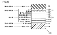
- FIG. 22 shows an electroluminescent element 100M of Example 45.
- a configuration of an electroluminescent element 100M shown in FIG. When compared with the electroluminescent device 100J shown in FIG. 19, the electroluminescent device 100M has an electroluminescent layer 10 as viewed from the first transparent electrode 11 side, an electron injection layer (EIL) 10a, an electron transport layer (ETL). ) 10b, a photon generation layer (EML) 10c, a hole transport layer (HTL) 10d, and a hole injection layer (HIL) 10e.
- EIL electron injection layer
- ETL electron transport layer
- HTL hole transport layer
- HIL hole injection layer
- the second transparent electrode 12 and the second transparent member 14 are closer to each other than when no transparent member is used while ensuring the electron injection performance and the transparency of the organic electroluminescent element. It is possible to ensure uneven light emission.
- FIG. 23 shows an electroluminescent device 100N as Example 46.
- FIG. This electroluminescent element 100N is a modification of the electroluminescent element 100M of FIG. 22 described above, and shows a configuration in which the first transparent electrode 11 is not limited to the cathode, and the first transparent electrode 11 may be the anode.
- the first transparent electrode 11 as an anode has a three-layer structure of transparent electrodes 11a and 11b using a conductive resin excellent in hole injection property and a transparent electrode 11b using silver (Ag).
- the light-emitting layer 10 includes a hole injection layer (HIL) 10e, a hole transport layer (HTL) 10d, a photon generation layer (EML) 10c, an electron transport layer (ETL) 10b, as viewed from the first transparent electrode 11 side. It has a five-layer structure of an electron injection layer (EIL) 10a.
- the second transparent electrode 12 as the cathode uses a conductive resin (perylene derivative) having a high electron injection property.
- FIG. 24 is a perspective view of the lighting device 200 in the present embodiment
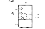
- FIG. 25 is a longitudinal sectional view of the lighting device 200 in the present embodiment.
- the illumination device 200 includes a main body housing 201 and a placement area 220 on which the illumination object 210 is placed.
- An outer window glass 300 is fitted in the mounting area 220.
- the outer window glass 300 is composed of the above-described electroluminescent element, and the second transparent electrode 12 and second transparent member 14 side of the electroluminescent element faces the mounting region 220.
- the lighting device 200 is a showcase for displaying children's toys, food (such as apples), and the like.
- the lighting device 200 is transparent and realizes light emission that is biased to one side (the mounting region 220 side), and functions as a transparent glass plate during quenching.
- the present invention is not limited to a showcase, and can be used, for example, as a lighting device for a house or a car window.
- the second transparent electrode 12 and the second transparent member 14 can be used as compared with the case where the transparent member is not used while ensuring the electron injection performance and the transparency of the organic electroluminescent device. It is possible to ensure light emission that is biased to the side.
- the driving voltage can be reduced and light can be emitted more efficiently.
- the value of the refractive index as described in the above embodiment, it is possible to emit light biased toward the second transparent electrode and the second transparent member while maintaining the electron injection property.
- a metal electrode for the first transparent electrode 11 it becomes possible to improve the electrode performance.
- the lighting device using the surface light emitting element based on the present embodiment emits little light to the human side who sees the exhibit, and the other side can be seen through, so that the space can be expanded and the lighting design is excellent. It becomes possible to realize a lighting device.
- Electroluminescent device 10 light emitting layer, 11 first transparent electrode, 11a, 11b, 11c, 12a , 12b transparent electrode, 12 second transparent electrode, 13 first transparent member, 14 second transparent member, 200 lighting device, 201 main body housing, 210 lighting object, 220 mounting area, 300 glass for outer window.
Landscapes
- Physics & Mathematics (AREA)
- Optics & Photonics (AREA)
- Electroluminescent Light Sources (AREA)
Description
図1および図2に、電界発光素子1を実現する最少の構成を示す。図1は、電界発光素子1の断面図であり、図2中のI-I線矢視断面に相当する。図2は、電界発光素子1の平面図である。
以下、図4および図5を参照して、本実施の形態における実施例1としての電界発光素子100Aについて説明する。図4は、本実施例における電界発光素子100Aの断面図、図5は、本実施例における電界発光素子100Aの発光層と各透明電極との界面における光の反射率の違いによる発光強度差を説明するための模式図である。図4の断面は、図2のI-I線矢視断面に相当する。
図4に示す電界発光素子100Aにおいて、発光層10で発光した光が第1透明部材13に遷移するのにかかる時間をτ1、発光層10で発光した光が第2透明部材14に遷移するのにかかる時間をτ2とする。


以下では、より具体的な実施例を用いて本実施の形態における電界発光素子を説明する。具体的な構成として可視光の領域(波長400nm~800nm)で発光する有機電界発光素子(有機EL)を用いた場合について説明する。
図6に、実施例2としての有機電界発光素子100B、図7に、実施例3としての有機電界発光素子100C、図8に、実施例4としての有機電界発光素子100Dを示す。図6から図8は、有機電界発光素子100B~100Dの断面構造を示す図である。


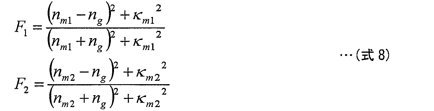


図8に、実施例4としての有機電界発光素子100Dの、材料の屈折率と膜厚、および発光層と透明電極の界面の反射率について、具体的な値を用いて詳しく説明する。
本実施の形態においては、2種類の透明電極を組み合わせて電子注入性をよくしつつ、透明性を確保しながら片側に発光強度を偏らせるために、透明部材の屈折率を本実施の形態の条件に設定することが本質である。
本実施の形態に基づいた他の実施の形態においては、透明電極として単膜に限らずに複数の膜を組み合わせてもよい。たとえば透明電極として金属薄膜を用いた場合には、導電性能を上げるために透明導電膜と組み合わせる構成が考えられる。図14および図15に他の実施例における電界発光素子の構造を示す。
本実施の形態の電界発光素子を用いた照明装置200について、図24および図25を参照して説明する。図24は、本実施の形態における照明装置200の斜視図、図25は、本実施の形態における照明装置200の縦断面図である。
Claims (12)
- 第1透明電極と、
第2透明電極と、
前記第1透明電極と前記第2透明電極とに挟まれた発光層と、
前記第1透明電極の前記発光層とは反対側の面に設けられる第1透明部材と、
前記第2透明電極の前記発光層とは反対側の面に設けられる第2透明部材と、を備え、
前記発光層から見た場合に、前記発光層と前記第1透明電極との界面の反射率が、前記発光層と前記第2透明電極との界面の反射率よりも高くなるように前記第1透明電極と前記第2透明電極との屈折率が選択され、
前記第1透明部材の屈折率が前記第2透明部材の屈折率よりも低くなるように設けられている、電界発光素子。 - 前記第1透明電極は、電子輸送性電極であり、前記第2透明電極は、正孔輸送性電極である、請求項1に記載の電界発光素子。
- 前記第1透明電極は、金属薄膜を含む、請求項1または2に記載の電界発光素子。
- 前記第1透明電極は、薄膜金属であり、
前記第2透明電極は、ITOである、請求項1に記載の電界発光素子。 - 前記第1透明電極は、前記第1透明部材側がITO、前記発光層側が薄膜金属の2層構造であり、
前記第2透明電極は、ITOである、請求項1に記載の電界発光素子。 - 前記第1透明電極は、前記第1透明部材側がITO、前記発光層側が薄膜金属の2層構造であり、
前記第2透明電極は、前記第2透明部材側および前記発光層側が導電性樹脂であり、2つの前記導電性樹脂に薄膜金属が挟み込まれる3層構造である、請求項1に記載の電界発光素子。 - 前記第1透明電極は、前記第1透明部材側が導電性樹脂、前記発光層側が薄膜金属の2層構造であり、
前記第2透明電極は、導電性樹脂である、請求項1に記載の電界発光素子。 - 前記第1透明電極は、前記第1透明部材側が導電性樹脂、前記発光層側が薄膜金属の2層構造であり、
前記第2透明電極は、前記第2透明部材側および前記発光層側が導電性樹脂であり、2つの前記導電性樹脂に薄膜金属が挟み込まれる3層構造である、請求項1に記載の電界発光素子。 - 前記第1透明電極は、前記第1透明部材側がITO、前記発光層側が導電性樹脂、前記ITOと前記導電性樹脂とに薄膜金属が挟み込まれる3層構造であり、
前記第2透明電極は、導電性樹脂である、請求項1に記載の電界発光素子。 - 前記第1透明電極は、前記第1透明部材側がITO、前記発光層側が薄膜金属の2層構造であり、
前記第2透明電極は、導電性樹脂である、請求項1に記載の電界発光素子。 - 前記第1透明電極は、前記第1透明部材側および前記発光層側が導電性樹脂であり、2つの前記導電性樹脂に薄膜金属が挟み込まれる3層構造であり、
前記第2透明電極は、導電性樹脂である、請求項1に記載の電界発光素子。 - 請求項1から11のいずれかに記載の電界発光素子を有する照明装置。
Priority Applications (3)
| Application Number | Priority Date | Filing Date | Title |
|---|---|---|---|
| EP13804209.8A EP2863714A4 (en) | 2012-06-14 | 2013-04-16 | ELECTROLUMINESCENT ELEMENT AND LIGHTING DEVICE WITH THIS ELECTROLUMINESCENCE ELEMENT |
| US14/407,613 US20150188078A1 (en) | 2012-06-14 | 2013-04-16 | Electroluminescent Element and Lighting Apparatus Comprising the Same |
| JP2014520991A JPWO2013187119A1 (ja) | 2012-06-14 | 2013-04-16 | 電界発光素子およびその電界発光素子を用いた照明装置 |
Applications Claiming Priority (2)
| Application Number | Priority Date | Filing Date | Title |
|---|---|---|---|
| JP2012-134790 | 2012-06-14 | ||
| JP2012134790 | 2012-06-14 |
Publications (1)
| Publication Number | Publication Date |
|---|---|
| WO2013187119A1 true WO2013187119A1 (ja) | 2013-12-19 |
Family
ID=49757957
Family Applications (1)
| Application Number | Title | Priority Date | Filing Date |
|---|---|---|---|
| PCT/JP2013/061240 Ceased WO2013187119A1 (ja) | 2012-06-14 | 2013-04-16 | 電界発光素子およびその電界発光素子を用いた照明装置 |
Country Status (4)
| Country | Link |
|---|---|
| US (1) | US20150188078A1 (ja) |
| EP (1) | EP2863714A4 (ja) |
| JP (1) | JPWO2013187119A1 (ja) |
| WO (1) | WO2013187119A1 (ja) |
Cited By (1)
| Publication number | Priority date | Publication date | Assignee | Title |
|---|---|---|---|---|
| WO2018008266A1 (ja) * | 2016-07-06 | 2018-01-11 | コニカミノルタ株式会社 | 電界発光素子 |
Families Citing this family (11)
| Publication number | Priority date | Publication date | Assignee | Title |
|---|---|---|---|---|
| KR20150001528A (ko) * | 2013-06-27 | 2015-01-06 | 삼성전자주식회사 | 수직형 유기 발광 트랜지스터 및 이를 구비한 유기 엘이디 조명장치 |
| US10276821B2 (en) * | 2015-10-30 | 2019-04-30 | National Taiwan University | Electroluminescent device |
| US10944072B2 (en) | 2015-11-03 | 2021-03-09 | Cornell University | Stretchable electroluminescent devices |
| TWI746603B (zh) * | 2016-08-09 | 2021-11-21 | 南韓商東友精細化工有限公司 | 透明電極、包括其的觸控感測器及影像顯示裝置 |
| DE102016219060A1 (de) * | 2016-09-30 | 2018-04-05 | Osram Oled Gmbh | Optoelektronische Vorrichtung mit Reflektionseigenschaft |
| JP7032740B2 (ja) * | 2017-02-08 | 2022-03-09 | 国立大学法人山形大学 | 組成物および有機光電子素子ならびにその製造方法 |
| US10522787B1 (en) * | 2018-11-27 | 2019-12-31 | Sharp Kabushiki Kaisha | High efficiency quantum dot LED structure |
| TW202541675A (zh) * | 2018-12-28 | 2025-10-16 | 日商半導體能源研究所股份有限公司 | 發光裝置、照明裝置、顯示裝置、模組及電子機器 |
| US20220209166A1 (en) * | 2019-04-11 | 2022-06-30 | Sharp Kabushiki Kaisha | Light-emitting element and display device |
| US20240172467A1 (en) * | 2021-06-01 | 2024-05-23 | Beijing Boe Technology Development Co., Ltd. | Electron Transport Layer Material and Preparation Method therefor, Electroluminescent Device and Preparation Method therefor, and Display Apparatus |
| KR20250081222A (ko) * | 2023-11-29 | 2025-06-05 | 엘지디스플레이 주식회사 | 유기 발광 소자 및 그를 이용한 표시 장치 |
Citations (9)
| Publication number | Priority date | Publication date | Assignee | Title |
|---|---|---|---|---|
| JPH10294182A (ja) | 1997-04-18 | 1998-11-04 | Idemitsu Kosan Co Ltd | 有機エレクトロルミネッセンス素子 |
| WO2004077386A1 (ja) * | 2003-02-28 | 2004-09-10 | Semiconductor Energy Laboratory Co., Ltd. | 表示装置、折り畳み型携帯端末 |
| JP2004265691A (ja) * | 2003-02-28 | 2004-09-24 | Semiconductor Energy Lab Co Ltd | 発光装置および電子機器 |
| JP2005129496A (ja) * | 2003-10-22 | 2005-05-19 | Hannstar Display Corp | 有機発光素子 |
| JP2006165034A (ja) * | 2004-12-02 | 2006-06-22 | Stanley Electric Co Ltd | 有機el素子 |
| JP2006253044A (ja) * | 2005-03-14 | 2006-09-21 | Fuji Electric Holdings Co Ltd | 有機elディスプレイおよびそのリーク修復方法 |
| JP2008130449A (ja) * | 2006-11-22 | 2008-06-05 | Alps Electric Co Ltd | 発光装置およびその製造方法 |
| JP2011065781A (ja) | 2009-09-15 | 2011-03-31 | Panasonic Electric Works Co Ltd | 面状発光装置 |
| JP2012015122A (ja) | 2005-10-18 | 2012-01-19 | Semiconductor Energy Lab Co Ltd | 電子機器 |
Family Cites Families (18)
| Publication number | Priority date | Publication date | Assignee | Title |
|---|---|---|---|---|
| US6778582B1 (en) * | 2000-03-06 | 2004-08-17 | Novalux, Inc. | Coupled cavity high power semiconductor laser |
| GB0016777D0 (en) * | 2000-07-07 | 2000-08-30 | Seos Displays Ltd | Improved film mirror |
| JP2002107746A (ja) * | 2000-09-28 | 2002-04-10 | Minolta Co Ltd | 表示パネル及びその製造方法 |
| JP4349784B2 (ja) * | 2002-10-01 | 2009-10-21 | パイオニア株式会社 | 画像表示装置及び製造方法 |
| EP1603367B1 (en) * | 2003-03-12 | 2015-09-09 | Mitsubishi Chemical Corporation | Electroluminescence device |
| JP3860582B2 (ja) * | 2003-07-31 | 2006-12-20 | 株式会社東芝 | 半導体装置の製造方法 |
| US7202504B2 (en) * | 2004-05-20 | 2007-04-10 | Semiconductor Energy Laboratory Co., Ltd. | Light-emitting element and display device |
| US20060004941A1 (en) * | 2004-06-30 | 2006-01-05 | Shah Hemal V | Method, system, and program for accessesing a virtualized data structure table in cache |
| US8008652B2 (en) * | 2004-09-24 | 2011-08-30 | Semiconductor Energy Laboratory Co., Ltd. | Light emitting device |
| JP4779845B2 (ja) * | 2006-07-14 | 2011-09-28 | ブラザー工業株式会社 | プリント装置 |
| GB2444081B (en) * | 2006-11-24 | 2011-05-11 | Ocuity Ltd | Manufacture of a birefringent liquid crystal component |
| KR101148886B1 (ko) * | 2009-05-13 | 2012-05-29 | 네오뷰코오롱 주식회사 | 유기전계발광소자 및 그 제조방법 |
| JP2011119233A (ja) * | 2009-11-04 | 2011-06-16 | Canon Inc | 有機el素子とそれを用いた表示装置 |
| KR20110118277A (ko) * | 2010-04-23 | 2011-10-31 | 한국전자통신연구원 | 투과형 유기 발광 다이오드 소자 및 이를 이용한 투과형 조명 장치 |
| WO2012017488A1 (ja) * | 2010-08-06 | 2012-02-09 | パナソニック株式会社 | 発光素子とその製造方法、および発光装置 |
| EP2619816A4 (en) * | 2010-09-24 | 2014-06-11 | Univ California | NANO WIRE POLYMER COMPOSITE ELECTRODES |
| US20130025194A1 (en) * | 2011-07-27 | 2013-01-31 | Paul Adam | Landscape edging system |
| JPWO2013094477A1 (ja) * | 2011-12-19 | 2015-04-27 | パナソニックIpマネジメント株式会社 | 透明導電膜、透明導電膜付き基材及びその製造方法 |
-
2013
- 2013-04-16 US US14/407,613 patent/US20150188078A1/en not_active Abandoned
- 2013-04-16 JP JP2014520991A patent/JPWO2013187119A1/ja active Pending
- 2013-04-16 WO PCT/JP2013/061240 patent/WO2013187119A1/ja not_active Ceased
- 2013-04-16 EP EP13804209.8A patent/EP2863714A4/en not_active Withdrawn
Patent Citations (9)
| Publication number | Priority date | Publication date | Assignee | Title |
|---|---|---|---|---|
| JPH10294182A (ja) | 1997-04-18 | 1998-11-04 | Idemitsu Kosan Co Ltd | 有機エレクトロルミネッセンス素子 |
| WO2004077386A1 (ja) * | 2003-02-28 | 2004-09-10 | Semiconductor Energy Laboratory Co., Ltd. | 表示装置、折り畳み型携帯端末 |
| JP2004265691A (ja) * | 2003-02-28 | 2004-09-24 | Semiconductor Energy Lab Co Ltd | 発光装置および電子機器 |
| JP2005129496A (ja) * | 2003-10-22 | 2005-05-19 | Hannstar Display Corp | 有機発光素子 |
| JP2006165034A (ja) * | 2004-12-02 | 2006-06-22 | Stanley Electric Co Ltd | 有機el素子 |
| JP2006253044A (ja) * | 2005-03-14 | 2006-09-21 | Fuji Electric Holdings Co Ltd | 有機elディスプレイおよびそのリーク修復方法 |
| JP2012015122A (ja) | 2005-10-18 | 2012-01-19 | Semiconductor Energy Lab Co Ltd | 電子機器 |
| JP2008130449A (ja) * | 2006-11-22 | 2008-06-05 | Alps Electric Co Ltd | 発光装置およびその製造方法 |
| JP2011065781A (ja) | 2009-09-15 | 2011-03-31 | Panasonic Electric Works Co Ltd | 面状発光装置 |
Non-Patent Citations (2)
| Title |
|---|
| RODNEY LOUDON: "The Quantum Theory of Light", 1994 |
| See also references of EP2863714A4 |
Cited By (2)
| Publication number | Priority date | Publication date | Assignee | Title |
|---|---|---|---|---|
| WO2018008266A1 (ja) * | 2016-07-06 | 2018-01-11 | コニカミノルタ株式会社 | 電界発光素子 |
| JPWO2018008266A1 (ja) * | 2016-07-06 | 2019-04-25 | コニカミノルタ株式会社 | 電界発光素子 |
Also Published As
| Publication number | Publication date |
|---|---|
| EP2863714A4 (en) | 2016-03-02 |
| US20150188078A1 (en) | 2015-07-02 |
| EP2863714A1 (en) | 2015-04-22 |
| JPWO2013187119A1 (ja) | 2016-02-04 |
Similar Documents
| Publication | Publication Date | Title |
|---|---|---|
| WO2013187119A1 (ja) | 電界発光素子およびその電界発光素子を用いた照明装置 | |
| Gather et al. | Recent advances in light outcoupling from white organic light-emitting diodes | |
| Saxena et al. | A review on the light extraction techniques in organic electroluminescent devices | |
| Liguori et al. | Overcoming challenges in OLED technology for lighting solutions | |
| US7982396B2 (en) | Light-emitting device with light-scattering particles and method of making the same | |
| TW200908780A (en) | Electroluminescent device having improved light output | |
| US7548021B2 (en) | OLED device having improved light output | |
| US20140061617A1 (en) | Method and apparatus for integrating an infrared (hr) pholovoltaic cell on a thin photovoltaic cell | |
| KR20100063730A (ko) | 유기 전계발광 소자 | |
| Zhou et al. | Ideal microlens array based on polystyrene microspheres for light extraction in organic light-emitting diodes | |
| JP6387828B2 (ja) | 電界発光素子およびその電界発光素子を用いた照明装置 | |
| US9806294B2 (en) | Surface light emitting element | |
| JP6287848B2 (ja) | 電界発光素子およびその電界発光素子を用いた照明装置 | |
| KR101825871B1 (ko) | 전계 발광 소자의 설계 방법 및 그 설계 방법을 사용한 전계 발광 소자의 제조 방법 | |
| JP2014086345A (ja) | 電界発光素子およびその電界発光素子を用いた照明装置 | |
| Zu Wang et al. | High performance optoelectronic device based on semitransparent organic photovoltaic cell integrated with organic light-emitting diode | |
| CN102447071B (zh) | 一种光栅结构有机发光二极管 | |
| KR101489780B1 (ko) | 유기발광다이오드 및 그 제조방법 | |
| CN110473975A (zh) | 一种交流驱动的双微腔顶发射白光有机电致发光器件 | |
| JP2013246932A (ja) | 面発光素子およびその面発光素子を用いた照明装置 | |
| Peng et al. | Improving light extraction of organic light‐emitting devices by attaching nanostructures with self‐assembled photonic crystal patterns | |
| JP2005327535A (ja) | 有機エレクトロルミネッセンス発光装置 | |
| KR20150035325A (ko) | 유기발광소자 | |
| KR102251945B1 (ko) | 유기발광 다이오드 | |
| JP2014232766A (ja) | 発光装置 |
Legal Events
| Date | Code | Title | Description |
|---|---|---|---|
| 121 | Ep: the epo has been informed by wipo that ep was designated in this application |
Ref document number: 13804209 Country of ref document: EP Kind code of ref document: A1 |
|
| ENP | Entry into the national phase |
Ref document number: 2014520991 Country of ref document: JP Kind code of ref document: A |
|
| WWE | Wipo information: entry into national phase |
Ref document number: 14407613 Country of ref document: US |
|
| NENP | Non-entry into the national phase |
Ref country code: DE |
|
| WWE | Wipo information: entry into national phase |
Ref document number: 2013804209 Country of ref document: EP |