WO2013187447A1 - 撮像装置及び撮像装置の制御方法 - Google Patents
撮像装置及び撮像装置の制御方法 Download PDFInfo
- Publication number
- WO2013187447A1 WO2013187447A1 PCT/JP2013/066245 JP2013066245W WO2013187447A1 WO 2013187447 A1 WO2013187447 A1 WO 2013187447A1 JP 2013066245 W JP2013066245 W JP 2013066245W WO 2013187447 A1 WO2013187447 A1 WO 2013187447A1
- Authority
- WO
- WIPO (PCT)
- Prior art keywords
- pixel
- phase difference
- difference detection
- pixel data
- data
- Prior art date
- Legal status (The legal status is an assumption and is not a legal conclusion. Google has not performed a legal analysis and makes no representation as to the accuracy of the status listed.)
- Ceased
Links
Images




Classifications
-
- G—PHYSICS
- G02—OPTICS
- G02B—OPTICAL ELEMENTS, SYSTEMS OR APPARATUS
- G02B7/00—Mountings, adjusting means, or light-tight connections, for optical elements
- G02B7/28—Systems for automatic generation of focusing signals
- G02B7/34—Systems for automatic generation of focusing signals using different areas in a pupil plane
-
- H—ELECTRICITY
- H04—ELECTRIC COMMUNICATION TECHNIQUE
- H04N—PICTORIAL COMMUNICATION, e.g. TELEVISION
- H04N23/00—Cameras or camera modules comprising electronic image sensors; Control thereof
- H04N23/60—Control of cameras or camera modules
- H04N23/67—Focus control based on electronic image sensor signals
-
- H—ELECTRICITY
- H04—ELECTRIC COMMUNICATION TECHNIQUE
- H04N—PICTORIAL COMMUNICATION, e.g. TELEVISION
- H04N23/00—Cameras or camera modules comprising electronic image sensors; Control thereof
- H04N23/60—Control of cameras or camera modules
- H04N23/67—Focus control based on electronic image sensor signals
- H04N23/672—Focus control based on electronic image sensor signals based on the phase difference signals
-
- H—ELECTRICITY
- H04—ELECTRIC COMMUNICATION TECHNIQUE
- H04N—PICTORIAL COMMUNICATION, e.g. TELEVISION
- H04N23/00—Cameras or camera modules comprising electronic image sensors; Control thereof
- H04N23/80—Camera processing pipelines; Components thereof
- H04N23/84—Camera processing pipelines; Components thereof for processing colour signals
- H04N23/843—Demosaicing, e.g. interpolating colour pixel values
-
- H—ELECTRICITY
- H04—ELECTRIC COMMUNICATION TECHNIQUE
- H04N—PICTORIAL COMMUNICATION, e.g. TELEVISION
- H04N25/00—Circuitry of solid-state image sensors [SSIS]; Control thereof
- H04N25/10—Circuitry of solid-state image sensors [SSIS]; Control thereof for transforming different wavelengths into image signals
- H04N25/11—Arrangement of colour filter arrays [CFA]; Filter mosaics
- H04N25/13—Arrangement of colour filter arrays [CFA]; Filter mosaics characterised by the spectral characteristics of the filter elements
- H04N25/134—Arrangement of colour filter arrays [CFA]; Filter mosaics characterised by the spectral characteristics of the filter elements based on three different wavelength filter elements
-
- H—ELECTRICITY
- H04—ELECTRIC COMMUNICATION TECHNIQUE
- H04N—PICTORIAL COMMUNICATION, e.g. TELEVISION
- H04N25/00—Circuitry of solid-state image sensors [SSIS]; Control thereof
- H04N25/40—Extracting pixel data from image sensors by controlling scanning circuits, e.g. by modifying the number of pixels sampled or to be sampled
- H04N25/42—Extracting pixel data from image sensors by controlling scanning circuits, e.g. by modifying the number of pixels sampled or to be sampled by switching between different modes of operation using different resolutions or aspect ratios, e.g. switching between interlaced and non-interlaced mode
-
- H—ELECTRICITY
- H04—ELECTRIC COMMUNICATION TECHNIQUE
- H04N—PICTORIAL COMMUNICATION, e.g. TELEVISION
- H04N25/00—Circuitry of solid-state image sensors [SSIS]; Control thereof
- H04N25/40—Extracting pixel data from image sensors by controlling scanning circuits, e.g. by modifying the number of pixels sampled or to be sampled
- H04N25/44—Extracting pixel data from image sensors by controlling scanning circuits, e.g. by modifying the number of pixels sampled or to be sampled by partially reading an SSIS array
- H04N25/445—Extracting pixel data from image sensors by controlling scanning circuits, e.g. by modifying the number of pixels sampled or to be sampled by partially reading an SSIS array by skipping some contiguous pixels within the read portion of the array
-
- H—ELECTRICITY
- H04—ELECTRIC COMMUNICATION TECHNIQUE
- H04N—PICTORIAL COMMUNICATION, e.g. TELEVISION
- H04N25/00—Circuitry of solid-state image sensors [SSIS]; Control thereof
- H04N25/40—Extracting pixel data from image sensors by controlling scanning circuits, e.g. by modifying the number of pixels sampled or to be sampled
- H04N25/46—Extracting pixel data from image sensors by controlling scanning circuits, e.g. by modifying the number of pixels sampled or to be sampled by combining or binning pixels
-
- H—ELECTRICITY
- H04—ELECTRIC COMMUNICATION TECHNIQUE
- H04N—PICTORIAL COMMUNICATION, e.g. TELEVISION
- H04N25/00—Circuitry of solid-state image sensors [SSIS]; Control thereof
- H04N25/60—Noise processing, e.g. detecting, correcting, reducing or removing noise
- H04N25/67—Noise processing, e.g. detecting, correcting, reducing or removing noise applied to fixed-pattern noise, e.g. non-uniformity of response
- H04N25/671—Noise processing, e.g. detecting, correcting, reducing or removing noise applied to fixed-pattern noise, e.g. non-uniformity of response for non-uniformity detection or correction
-
- H—ELECTRICITY
- H04—ELECTRIC COMMUNICATION TECHNIQUE
- H04N—PICTORIAL COMMUNICATION, e.g. TELEVISION
- H04N25/00—Circuitry of solid-state image sensors [SSIS]; Control thereof
- H04N25/70—SSIS architectures; Circuits associated therewith
- H04N25/703—SSIS architectures incorporating pixels for producing signals other than image signals
- H04N25/704—Pixels specially adapted for focusing, e.g. phase difference pixel sets
-
- H—ELECTRICITY
- H04—ELECTRIC COMMUNICATION TECHNIQUE
- H04N—PICTORIAL COMMUNICATION, e.g. TELEVISION
- H04N5/00—Details of television systems
- H04N5/222—Studio circuitry; Studio devices; Studio equipment
- H04N5/262—Studio circuits, e.g. for mixing, switching-over, change of character of image, other special effects ; Cameras specially adapted for the electronic generation of special effects
- H04N5/265—Mixing
-
- H—ELECTRICITY
- H04—ELECTRIC COMMUNICATION TECHNIQUE
- H04N—PICTORIAL COMMUNICATION, e.g. TELEVISION
- H04N2209/00—Details of colour television systems
- H04N2209/04—Picture signal generators
- H04N2209/041—Picture signal generators using solid-state devices
- H04N2209/042—Picture signal generators using solid-state devices having a single pick-up sensor
- H04N2209/045—Picture signal generators using solid-state devices having a single pick-up sensor using mosaic colour filter
Definitions
- the present invention relates to an imaging apparatus that detects a focus state by using a part of pixels as a phase difference detection element of a phase difference method, and a control method thereof.
- Japanese Patent No. 3592147 proposes an imaging apparatus that detects a focus state by using a part of pixels of an imaging element as a phase difference detection element.
- An imaging apparatus proposed in Japanese Patent No. 3592147 sets a part of pixels of an imaging element as a phase difference detection pixel, and passes through a different pupil region symmetric with respect to the optical axis center of the photographing lens.
- the light beam is focused on a plurality of phase difference detection pixels, and the focus state of the photographing lens is detected by detecting the phase difference between the subject light beams.
- the phase difference detection pixel becomes a defective pixel that cannot be used as an image as it is. Therefore, in Japanese Patent No. 3592147, the output signal of the phase difference detection pixel is interpolated using the output signal of the surrounding same color pixel. However, if such an interpolation process is performed on a subject having a high spatial frequency, the sharpness of the image is lowered.
- the imaging apparatus disclosed in Japanese Patent Application Laid-Open No. 2010-062640 detects variations (spatial frequency) of signals of pixels around the phase difference detection pixel, and the gain adjustment amount and the interpolation correction amount based on the detection result. To determine the percentage of.
- the above-described imaging apparatus disclosed in Japanese Patent Application Laid-Open No. 2010-062640 changes the ratio between the gain adjustment amount and the interpolation correction amount in accordance with variations in output signals of pixels around the phase difference detection pixel.
- the ratio of the correction amount is changed with uniform judgment for each phase difference detection pixel, overcorrection may occur depending on the method of signal readout from the image sensor, and image quality may be deteriorated more than when correction is not performed. is there.
- the present invention has been made in view of the above circumstances, and in an imaging apparatus including an imaging element having a phase difference detection pixel, an imaging apparatus capable of suppressing deterioration in image quality due to the phase difference detection pixel and a control method thereof
- the purpose is to provide.
- an imaging device includes an imaging device in which a phase difference detection pixel for focus detection is arranged at a partial position of the imaging pixel, and the imaging device.
- a reading method setting unit that sets a reading method when reading pixel data from the imaging pixel and the phase difference detection pixel, and an image processing unit that corrects the pixel data of the phase difference detection pixel, and
- the image processing unit applies an application ratio of the pixel data of the phase difference detection pixel read according to the reading method set by the reading method setting unit and the interpolation data from the pixel data around the phase difference detection pixel
- the correction processing is performed so as to switch between.
- the image pickup apparatus control method includes an image pickup element in which phase difference detection pixels for focus detection are arranged at some positions of the image pickup pixels.
- a readout method setting unit for reading out pixel data from the imaging pixel and the phase difference detection pixel, and the phase difference read from the imaging device according to the set readout method. Correction processing by the image processing unit so as to switch the application ratio between the pixel data of the detection pixel and the interpolation data from the pixel data around the phase difference detection pixel.
- FIG. 1 is a block diagram illustrating a configuration of a digital camera as an example of an imaging apparatus according to an embodiment of the present invention.
- FIG. 2 is a diagram illustrating a detailed configuration of the imaging control circuit and the image processing unit.
- FIG. 3 is a diagram illustrating a pixel array of the image sensor.
- FIG. 4A is a diagram illustrating an image formation state in an imaging pixel.
- FIG. 4B is a diagram illustrating an image formation state of the phase difference detection pixel.
- FIG. 5 is a flowchart illustrating a moving image recording operation process performed by the imaging apparatus.
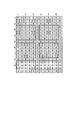
- FIG. 6A is a diagram showing a pixel arrangement before 2 ⁇ 2 pixel mixed readout.
- FIG. 6B is a diagram illustrating a pixel arrangement after 2 ⁇ 2 pixel mixed readout.
- FIG. 7A is a diagram illustrating a pixel arrangement before 3 ⁇ 3 pixel mixed readout.
- FIG. 7B is a diagram illustrating a pixel arrangement after 3 ⁇ 3 pixel mixed readout.
- FIG. 8 is a flowchart showing pixel interpolation processing.
- FIG. 1 is a block diagram illustrating a configuration of a digital camera (hereinafter simply referred to as a camera) as an example of an imaging apparatus according to an embodiment of the present invention.
- a solid line with an arrow indicates a data flow
- a broken line with an arrow indicates a control signal flow.
- the camera 1 shown in FIG. 1 includes a photographic lens 11, an aperture 13, a mechanical shutter 15, a drive unit 17, an operation unit 19, an image sensor 21, an imaging control circuit 23, an A-AMP 25, and analog-digital conversion.
- Unit (ADC) 27, CPU (Central Processing Unit) 29, image processing unit 31, focus detection circuit 33, video encoder 35, display unit 37, bus 39, DRAM (Dynamic Random Access Memory) 41 A ROM (Read Only Memory) 43 and a recording medium 45.
- ADC Central Processing Unit
- CPU Central Processing Unit
- focus detection circuit 33 video encoder 35
- display unit 37 bus 39
- DRAM Dynamic Random Access Memory
- ROM Read Only Memory
- the photographing lens 11 has a single lens or a plurality of lenses for forming an image from the subject 100 on the image sensor 21.
- the taking lens 11 may be a single focus lens or a zoom lens.
- the diaphragm 13 is disposed on the optical axis of the photographic lens 11 and has a variable aperture. The diaphragm 13 limits the amount of light flux from the subject 100 that has passed through the photographing lens 11.
- the mechanical shutter 15 is disposed behind the diaphragm 13 and is configured to be freely opened and closed.
- the mechanical shutter 15 adjusts the incident time of the subject luminous flux from the subject 100 to the image sensor 21 (exposure time of the image sensor 21) by adjusting the opening time.
- a known focal plane shutter, lens shutter, or the like can be employed as the mechanical shutter 15.
- the driving unit 17 performs focus adjustment of the photographing lens 11, aperture diameter control of the diaphragm 13, and opening / closing control of the mechanical shutter 15 based on a control signal from the CPU 29.
- the operation unit 19 includes various operation buttons such as a power button, a release button, a reproduction button, and a menu button, and various operation members such as a touch panel.
- the operation unit 19 detects operation states of various operation members and outputs a signal indicating the detection result to the CPU 29.
- the shooting mode of the camera 1 can be selected by the operation unit 19 of the present embodiment. That is, the user can select the shooting mode of the camera 1 from either the still image shooting mode or the moving image shooting mode by operating a shooting mode dial as an operation member included in the operation unit 19.
- the still image shooting mode is a shooting mode for shooting a still image
- the moving image shooting mode is a shooting mode for shooting a moving image.
- an example in which selection is made with a dial is shown, but the shooting mode may be selected by, for example, operating a touch panel on a menu screen.
- the imaging element 21 is disposed on the optical axis of the photographing lens 11, behind the mechanical shutter 15, and at a position where the subject light beam is imaged by the photographing lens 11.
- the image sensor 21 is configured by two-dimensionally arranging photodiodes that constitute pixels.
- the image sensor 21 in the present embodiment includes an image pickup pixel for acquiring an image for recording and display and a phase difference detection pixel for focus detection.
- the photodiode that constitutes the image sensor 21 generates a charge corresponding to the amount of received light.
- the electric charge generated in the photodiode is accumulated in a capacitor connected to each photodiode.
- the electric charge accumulated in this capacitor is read out as an image signal.
- the image sensor 21 in the present embodiment has a plurality of different charge readout methods.
- the charge accumulated in the image sensor 21 is read according to a control signal from the image capture control circuit 23.
- a Bayer array color filter is disposed on the front surface of the photodiode constituting the pixel.
- the Bayer array has a line in which R pixels and G (Gr) pixels are alternately arranged in the horizontal direction, and a line in which G (Gb) pixels and B pixels are alternately arranged.
- the phase difference detection pixels are arranged at some positions of the imaging pixels. Unlike the other pixels, the pixels used as the phase difference detection pixels shield some areas. Details of the image sensor 21 will be described later.
- the imaging control circuit 23 sets the readout method of the imaging device 21 according to the control signal from the CPU 29, and controls the readout of the image signal from the imaging device 21 according to the set readout method. Details of the imaging control circuit 23 will be described later in detail.
- the A-AMP 25 adjusts the analog gain of the image signal output from the image sensor 21.
- the ADC 27 is an analog-digital converter, and converts the image signal whose analog gain has been adjusted by the A-AMP 25 into a digital image signal (pixel data).
- pixel data a collection of a plurality of pixel data is referred to as imaging data in this specification.
- the CPU 29 performs overall control of the camera 1 according to a program stored in the ROM 43 described later.
- the image processing unit 31 performs various types of image processing on the captured data to generate image data. For example, when recording a still image, the image processing unit 31 performs still image recording image processing to generate still image data. Similarly, when recording a moving image, the image processing unit 31 performs moving image recording image processing to generate moving image data. Furthermore, the image processing unit 31 performs display image processing during live view display to generate display image data. The detailed configuration of the image processing unit 31 will be described in detail later.
- the focus detection circuit 33 acquires pixel data from the phase difference detection pixel, and calculates a defocus direction and a defocus amount with respect to the in-focus position of the photographing lens 11 using a known phase difference method based on the acquired pixel data. To do.
- the video encoder 35 reads the display image data generated by the image processing unit 31 and temporarily stored in the DRAM 41, and outputs the read display image data to the display unit 37.
- the display unit 37 is a display unit such as a liquid crystal display or an organic EL display, and is disposed on the back surface of the camera 1, for example.
- the display unit 37 displays an image according to the display image data input from the video encoder 35.
- the display unit 37 is used for live view display, display of recorded images, and the like.
- the bus 39 is connected to the ADC 27, the CPU 29, the image processing unit 31, the focus detection circuit 33, the video encoder 35, the DRAM 41, the ROM 43, and the recording medium 45. On the bus 39, various data generated in these blocks are transferred.
- the DRAM 41 is an electrically rewritable memory, and temporarily stores various data such as the above-described imaging data (pixel data), recording image data, display image data, and processing data in the CPU 29.
- SDRAM Serial Dynamic Random Access Memory
- the ROM 43 is a non-volatile memory such as a mask ROM or a flash memory.
- the ROM 43 stores various data such as a program used by the CPU 29 and adjustment values of the camera 1.
- the recording medium 45 is configured to be built in or freely loaded in the camera 1 and records recording image data as an image file of a predetermined format.
- FIG. 2 is a diagram illustrating a detailed configuration of the imaging control circuit 23 and the image processing unit 31.
- a solid line with an arrow indicates a flow of imaging data (pixel data).
- a broken line with an arrow indicates a flow of setting data for the imaging control circuit 23
- an alternate long and short dash line with an arrow indicates a flow of RGB data (a result of simultaneous processing of imaging data)
- a two-dot chain line with an arrow indicates YC data ( The flow of RGB data) is represented respectively.
- RGB data or YC data corresponds to the image data described above.
- the imaging control circuit 23 various settings are made according to the readout method of the pixel data from the imaging element 21.
- the imaging control circuit 23 outputs a control signal for reading pixel data from the imaging device 21 to the imaging device 21 in accordance with this setting.
- Such an imaging control circuit 23 includes a readout method setting unit 231 and a mixing rate setting unit 232.
- the readout method of the pixel data from the image sensor 21 is set according to the setting data from the CPU 29.
- the readout method is set according to the operating state of the camera 1. For example, when real-time performance is required for reading pixel data from the image sensor 21 (for example, during live view display or moving image recording), pixel data from a plurality of pixels of the same color is used so that the pixel data can be read at high speed. Are read out, or the pixel data of a specific pixel is read out. On the other hand, when image quality is required rather than real-time characteristics (for example, when recording a still image), resolution is maintained by reading pixel data of all pixels without performing mixed readout or thinning readout.
- the CPU 29 determines the operating state of the camera 1 and generates setting data so that a reading method according to the determined result is obtained.
- the horizontal and vertical pixel reading intervals when the pixel data is mixed or when the pixel data is thinned are set.
- a readout method (2 ⁇ 2 pixel mixed readout) in which a total of 4 pixels are mixed by 2 horizontal and vertical 2 pixels to 1 pixel, or a total of 4 pixels of 2 horizontal and 2 vertical pixels are thinned to 1 pixel.
- the readout method (2 ⁇ 2 pixel thinning readout) is set in the readout method setting unit 231, 2 is set for each of the horizontal readout interval and the vertical readout interval.
- the image processing unit 31 includes a gain adjustment unit 311, an interpolation ratio determination unit 312, a pixel interpolation unit 313, a development processing unit 314, and a color conversion processing unit 315.
- the image processing unit 31 also includes a compression / decompression processing unit and the like.
- the gain adjustment unit 311 performs gain adjustment of pixel data from the phase difference detection pixels. A partial region of the phase difference detection pixel is shielded. For this reason, even when a part of the subject having the same luminance is imaged, the amount of light incident on the phase difference detection pixel is smaller than the amount of light incident on the imaging pixel.
- the gain adjustment unit 311 performs correction to compensate for the dimming of pixel data that occurs by blocking a partial region of the phase difference detection pixel.
- the interpolation ratio determination unit 312 determines the pixel data of the phase difference detection pixel from the mixing rate calculated according to the reading method set in the reading method setting unit 231 and the horizontal / vertical reading interval set in the mixing rate setting unit 232. Determine the application rate.
- the application ratio is a weighting coefficient for weighted addition of the pixel data of the phase difference detection pixel subjected to gain adjustment processing and the pixel data around the phase difference detection pixel. Specifically, in the case of a readout method in which the pixel data mixture rate of the phase difference detection pixel is high, the pixel data of the phase difference detection pixel that has been subjected to gain adjustment processing by increasing the weighting coefficient of the pixel data of the peripheral pixels. Reduce the weighting coefficient.
- the pixel interpolation unit 313 performs a correction process on the pixel data of the phase difference detection pixel based on the application ratio (weighting coefficient) determined by the interpolation ratio determination unit 312.
- the development processing unit 314 performs synchronization processing (demosaicing processing), NR (Noise Reduction) processing, WB (White Balance) correction, edge enhancement processing, and the like on the imaging data including the pixel data interpolated by the pixel interpolation unit 313. Apply.
- synchronization processing demosaicing processing
- NR Noise Reduction
- WB White Balance
- edge enhancement processing edge enhancement processing, and the like on the imaging data including the pixel data interpolated by the pixel interpolation unit 313.
- the color conversion processing unit 315 performs processing for generating display image data or recording image data from the RGB data obtained in the development processing unit 314. This processing includes, for example, processing for converting RGB data into YC data by matrix calculation, gamma correction processing for YC data, and the like.
- FIG. 3 is a diagram illustrating a pixel array of the image sensor 21.
- a part of the pixels is shown in an enlarged manner.
- FIG. 3 shows an example of the Bayer arrangement, but the arrangement of the color filters is not limited to the Bayer arrangement, and various arrangements can be applied.
- the Bayer array image sensor 21 has a line in which R pixels and G (Gr) pixels are alternately arranged in the horizontal direction and a line in which G (Gb) pixels and B pixels are alternately arranged. is doing.
- a set of four pixels of the Gr pixel, the R pixel, the Gb pixel, and the B pixel shown in the enlarged view on the right side is repeatedly arranged in the horizontal and vertical directions.
- phase difference detection pixels are arranged at the positions of some imaging pixels.
- the phase difference detection pixel is, for example, a pixel in which one of the left and right regions is shielded by a light shielding film.
- a row of phase difference detection pixels hereinafter referred to as right opening phase difference detection pixels
- a phase difference detection pixel hereinafter referred to as left opening phase difference detection
- phase difference detection pixels In the case of an image sensor with a large number of pixels, the area of each pixel is small, so it can be considered that the same image is formed on pixels arranged close to each other. Therefore, by arranging the phase difference detection pixels as shown in FIG. 3, the phase difference can be detected by a pair of the phase difference detection pixels in the A row and the B phase difference detection pixels in FIG. The phase difference can also be detected by a pair of phase difference detection pixels in the C row and phase difference detection pixels in the D row.
- the light-shielding region in the phase difference detection pixel is set to either the left or right region. In this case, it is possible to detect the horizontal phase difference. On the other hand, it is also possible to detect a vertical phase difference or a phase difference in an oblique direction by setting a light shielding region as an upper or lower region or an oblique region. Further, as long as it has a certain area, the light shielding area may not be 1/2 of the pixel region. Further, in FIG. 3, the phase difference detection pixel is arranged in the G pixel, but it may be arranged in any of the R pixel and the B pixel other than the G pixel.
- FIG. 3 shows an example in which pupil division is performed by shielding a partial area of the phase difference detection pixel 21b, but the phase difference detection pixel is a pair of pixels that have passed through different pupil areas of the photographing lens 11. It is only necessary to selectively receive one of the subject luminous fluxes forming For this reason, instead of a configuration in which a partial region is shielded from light, for example, pupil division may be performed by a pupil division microlens.
- FIG. 4A shows an imaging state of an image in the imaging pixel 21a.
- FIG. 4B shows an image formation state of the image in the phase difference detection pixel 21b.
- the photographing lens 11 when the photographing lens 11 is in a focused state, a pair of subject luminous fluxes emitted from the subject and passing through different pupil regions symmetric with respect to the optical axis center of the photographing lens 11 are imaged. An image is formed at the same position on the element 21.
- the peak position of the image formed on the imaging pixel 21a matches the peak position of the image formed on the phase difference detection pixel 21b.
- a part of the region of the phase difference detection pixel 21b is shielded from light, only the peak of one image of a pair of subject light beams is detected. For this reason, a decrease in the amount of light occurs in the phase difference detection pixel 21b.
- a pair of subject luminous fluxes emitted from the subject and passing through different pupil regions of the photographing lens 11 form images at different positions on the image sensor 21.
- an image corresponding to each of the subject luminous fluxes that have passed through different pupil regions is formed on the imaging pixel 21a.
- only an image corresponding to one of the subject luminous fluxes passing through different pupil regions is formed on the phase difference detection pixel 21b.
- the peak position of the image formed on the imaging pixel 21a and the peak position of the image formed on the phase difference detection pixel 21b do not coincide with each other, and an image shift occurs.
- the amount of light also decreases.
- FIG. 5 is a flowchart showing the process of moving image recording (moving image shooting) operation by the imaging apparatus.
- the moving image recording operation is started, for example, when the release button is pressed during the moving image shooting mode. 5 is executed by the CPU 29 according to a program stored in the ROM 43. Note that FIG. 5 shows the operation at the time of moving image recording, but the imaging control method of the present embodiment described below can also be applied at the time of still image recording or live view display.
- the CPU 29 starts taking in the imaging data (step S101).
- the CPU 29 inputs setting data corresponding to the current operation mode to the reading method setting unit 231 of the imaging control circuit 23.
- the imaging control circuit 23 controls reading of pixel data from the imaging element 21.
- the setting data corresponding to the readout method at the time of moving image recording is input.
- the mixing rate setting unit 232 sets the horizontal and vertical pixel reading intervals when mixing or thinning out pixel data. For example, in the case of 2 ⁇ 2 pixel mixed readout or 2 ⁇ 2 pixel thinning readout, 2 is set for each of the horizontal readout interval and the vertical readout interval. In the case of 3 ⁇ 3 pixel mixed readout or 3 ⁇ 3 pixel thinning readout, 3 is set for each of the horizontal readout interval and the vertical readout interval.
- an image signal in a state of pixel mixture or pixel thinning is read out from the imaging device 21 in accordance with the readout method set in the imaging control circuit 23.
- the image signal read from the image sensor 21 is digitized by the ADC 27 and then temporarily stored in the DRAM 41 as image data.
- the CPU 29 performs focus detection processing (step S102).
- the CPU 29 causes the focus detection circuit 33 to execute focus detection processing.
- the focus detection circuit 33 reads out pixel data corresponding to the phase difference detection pixel (mixed or thinned out) from the imaging data temporarily stored in the DRAM 41, and uses this pixel data as the pixel data.
- the defocus direction and defocus amount of the photographic lens 11 are calculated using a known phase difference method.
- the CPU 29 performs a mixing rate calculation process (step S103).
- the CPU 29 calculates the mixing rate, which is a value necessary for the interpolation rate determination unit 312 to determine the interpolation rate.
- the mixing rate is the mixing rate of the pixel data of the phase difference detection pixel in each pixel data after the pixel mixture reading or the pixel thinning-out reading.
- FIG. 6A is a diagram showing a pixel arrangement before 2 ⁇ 2 pixel mixed readout.
- FIG. 6B is a diagram showing a pixel arrangement after 2 ⁇ 2 pixel mixed readout.
- the numbers attached to the upper side and the left side of FIGS. 6A and 6B indicate the coordinates of the pixel. In the following description, it is assumed that two horizontal and vertical pixels including R pixels with numbers are the same coordinates.
- r shown in FIG. 6A indicates a phase difference detection pixel (right opening phase difference detection pixel) whose left half surface is shielded
- l shown in FIG. 6A is a phase difference detection pixel (left) whose right half surface is shielded.
- r shown in the left diagram of FIG. 6B indicates that the right aperture phase difference detection pixel is mixed in that pixel
- l shown in the left diagram of FIG. 6B indicates that the left aperture phase difference detection is detected in that pixel. Indicates that a pixel is mixed.
- the numbers attached to r and l in FIG. 6B indicate the number of right aperture phase difference detection pixels or left aperture phase difference detection pixels mixed in the pixels. Furthermore, the numbers shown on the right side of FIG. 6B indicate the total number of phase difference detection pixels mixed in each pixel.
- FIG. Pixel data of the R pixel at the coordinates (1, 1) is obtained.
- Other colors other than the R pixel are mixed in the same manner.
- the phase difference detection pixel is arranged at the position of the G (Gb) pixel
- the pixel data of the phase difference detection pixel is mixed into the pixel data after addition.
- the pixel data in the thick frame in FIG. 6A are mixed, the pixel data of the phase difference detection pixel is mixed.
- phase difference detection pixel in the case of 2 ⁇ 2 pixel mixed readout, pixel data of each phase difference detection pixel is mixed into the pixel data at each Gb position after mixing.
- a pixel mixed with pixel data of such a phase difference detection pixel can be used as a phase difference detection pixel even after mixed reading.
- FIG. 7A is a diagram showing pixel data before 3 ⁇ 3 pixel mixed readout.
- FIG. 7B is a diagram showing pixel data after 3 ⁇ 3 pixel mixed readout.
- pixel data of the same color for each horizontal and vertical pixel is mixed.
- the coordinates (2, 1), coordinates (2, 2), coordinates (2, 3), coordinates (3, 1), (3, 2), (3, 3), (4, 1) shown in FIG. ), (4, 2), and (4, 3) of the nine R pixel data are mixed to obtain the pixel data of the R pixel at the coordinates (1, 1) in FIG. 7B.
- Other colors other than the R pixel are mixed in the same manner.
- the pixel data of the first row is not used for mixing, but the pixel data of the first row may be used for mixing.
- the phase difference detection pixel is arranged at the position of the G (Gb) pixel
- the pixel data of the phase difference detection pixel is mixed into the pixel data after addition. Is done. That is, when the pixel data in the thick frame in FIG. 7A are mixed, the pixel data of the phase difference detection pixel is mixed.
- FIG. 7B in the case of 3 ⁇ 3 pixel mixed readout, the number of pixel data of the phase difference detection pixels mixed depending on the position is different.
- the number of pixel data of the phase difference detection pixels included in the pixel data after readout is n
- the horizontal readout interval at the time of pixel mixing or pixel decimation is h
- the vertical readout interval at the time of pixel mixing or pixel decimation is calculated for each pixel position according to the following (Equation 1).
- ⁇ n / (h ⁇ v) (Formula 1)
- ⁇ is 1 ⁇ 4 regardless of the position of the Gb pixel.
- ⁇ 3 ⁇ 3 pixel mixed readout ⁇ changes between 1/9 and 4/9 according to the position of the Gb pixel.
- the above example shows an example in which the mixing rate is calculated for each moving image recording, but the mixing rate for each reading method may be calculated in advance. In this case, it is only necessary to acquire the corresponding mixing rate when the reading method is set.
- the CPU 29 performs gain adjustment processing (step S104).
- the CPU 29 causes the gain adjustment unit 311 of the image processing unit 31 to perform gain adjustment.
- the gain adjustment amount is determined in consideration of the pixel data mixing rate of the phase difference detection pixels. In order to simplify the description, assuming that the amount of light is 1/2 in a phase difference detection pixel that shields either the left or right region as shown in FIG. 3, the gain adjustment amount ⁇ is given by the following (formula 2). .
- ⁇ (h ⁇ v) / ((h ⁇ v) ⁇ n ⁇ 0.5) (Formula 2)
- ⁇ is 4 / 3.5 regardless of the position of the Gb pixel.
- ⁇ changes between 9 / 8.5 and 9/7 depending on the position of the Gb pixel.
- the specific process of the gain adjustment process is a process of multiplying the value of the pixel data of the phase difference detection pixel by the gain adjustment amount ⁇ obtained by (Equation 2).
- Equation 2 assumes that the amount of light in the phase difference detection pixel is 1/2. Actually, the amount of light reduction varies depending on the aperture of the taking lens 11, the aperture of the diaphragm 13, and the like. Therefore, it is desirable that 0.5 in (Equation 2) is adaptively switched according to the aperture of the taking lens 11, the aperture of the diaphragm 13, and the like.
- the CPU 29 performs pixel interpolation processing (step S105).
- the CPU 29 causes the interpolation ratio determination unit 312 and the pixel interpolation unit 313 of the image processing unit 31 to perform pixel interpolation processing.
- the pixel interpolation process will be described in detail later.
- the CPU 29 performs lens driving (step S106).
- the CPU 29 controls the drive unit 17 based on the defocus direction and the defocus amount of the photographing lens 11 detected by the focus detection circuit 33 in step S102, and focuses the photographing lens 11.
- the CPU 29 performs image processing (step S107).
- the CPU 29 causes the development processing unit 314 and the color conversion processing unit 315 of the image processing unit 31 to execute the development processing and color conversion processing on the imaging data temporarily stored in the DRAM 41 as a result of the pixel interpolation processing in step S105.
- Processing parameters used for development processing and color conversion processing are those for recording.
- the processing parameters for recording are stored in advance in the ROM 43, for example.
- the CPU 29 records the image data temporarily stored in the DRAM 41 as a result of the image processing on the recording medium 45 (step S108).
- the CPU 29 determines whether or not to stop moving image recording (step S109).
- the CPU 29 determines the operation state of the release button of the operation unit 19. That is, when the release button is pressed again, the CPU 29 determines to stop moving image recording.
- step S109 When it is determined in step S109 that the moving image recording is not stopped, the CPU 29 returns the process to step S101 and continues the moving image recording. On the other hand, when it is determined in step S109 that the moving image recording is to be stopped, the CPU 29 ends the process of FIG.
- FIG. 8 is a flowchart showing details of pixel interpolation processing.
- the pixel interpolation process is a process performed mainly by the interpolation ratio determination unit 312 and the pixel interpolation unit 313.
- the interpolation ratio determination unit 312 determines whether or not pixel data of the phase difference detection pixel is included in the imaging data to be processed (step S201).
- the coordinate data of the phase difference detection pixel is stored in advance in the ROM 43, for example, and the interpolation ratio determination unit 312 determines whether or not the pixel data of the phase difference detection pixel is included in the imaging data to be processed from this coordinate data. judge.
- whether or not the pixel data of the phase difference detection pixel is included in the pixel data after reading is also determined by the reading method.
- the interpolation ratio determination unit 312 acquires the setting data of the readout method setting unit 231 and the mixing rate setting unit 232, refers to the coordinate data of the phase difference detection pixels according to the acquired setting data, and sets the imaging data. It is determined whether or not pixel data of the phase difference detection pixel is included.
- step S201 If it is determined in step S201 that the pixel data of the phase difference detection pixel is not included in the imaging data to be processed, the processing in FIG. 8 is terminated.
- step S201 when it is determined that the imaging data to be processed includes the pixel data of the phase difference detection pixel, the interpolation ratio determination unit 312 determines the mixing rate ⁇ calculated by the above-described mixing rate calculation process. Is acquired (step S202).
- correct_pixel af_pixel_weight ⁇ af_pixel + near_pixel_weight ⁇ (pixel_h_1 + pixel_h_2 + pixel_v_1 + pixel_v_2) (Formula 4) “Correct_pixel” in (Expression 4) indicates the value of the corrected pixel data after weighted addition. Further, af_pixel indicates the value of pixel data of the phase difference detection pixel (actually pixel data of the pixel including the phase difference detection pixel). Pixel_h_1 indicates the value of pixel data of the same color pixel of the left + 1 pixel of the phase difference detection pixel (pixel data on the upper left in the case of the Bayer array).
- Pixel_h_2 indicates the value of the pixel data of the same color pixel of the right + 1 pixel of the phase difference detection pixel (pixel data on the lower right in the case of the Bayer array).
- pixel_v_1 indicates the value of pixel data of the same color pixel of the upper +1 pixel of the phase difference detection pixel (pixel data on the upper right in the case of the Bayer array).
- pixel_v_2 indicates the value of pixel data of the same color pixel of the lower +1 pixel of the phase difference detection pixel (pixel data on the lower left in the case of the Bayer array).
- Equation 4 The weighted addition shown in (Equation 4) is performed for each phase difference detection pixel. After the weighted addition shown in (Equation 4) is performed for all the phase difference detection pixels, the processing in FIG. 8 ends.
- the present embodiment when pixel mixing or pixel thinning is performed, according to the mixing ratio of the pixel data of the phase difference detection pixel in each phase difference detection pixel after pixel mixing or after pixel thinning, The application ratio between the pixel data of each phase difference detection pixel and the interpolation data from the surrounding pixel data is changed.
- the pixel data mixture rate of the phase difference detection pixel is low, the application ratio of the pixel data of the phase difference detection pixel after gain adjustment is high, so that overcorrection does not occur and the sharpness of the image is reduced. Can be suppressed.
- the pixel data mixture rate of the phase difference detection pixel is high, the application ratio of the pixel data of the peripheral pixels is high, so that it is possible to suppress the influence of image shift caused by using the phase difference detection pixel. It is.
- each process according to the above-described embodiment can be stored as a program that can be executed by the CPU 29.
- memory cards ROM cards, RAM cards, etc.
- magnetic disks floppy disks, hard disks, etc.
- optical disks CD-ROM, DVD, etc.
- storage media of external storage devices such as semiconductor memories, etc. are distributed. be able to.
- the CPU 29 can execute the above-described processing by reading a program stored in the storage medium of the external storage device and controlling the operation by the read program.
- the above-described embodiments include inventions at various stages, and various inventions can be extracted by appropriately combining a plurality of disclosed constituent elements. For example, even if some configuration requirements are deleted from all the configuration requirements shown in the embodiment, the above-described problem can be solved, and this configuration requirement is deleted when the above-described effects can be obtained.
- the configuration can also be extracted as an invention.
Landscapes
- Engineering & Computer Science (AREA)
- Multimedia (AREA)
- Signal Processing (AREA)
- Physics & Mathematics (AREA)
- General Physics & Mathematics (AREA)
- Optics & Photonics (AREA)
- Spectroscopy & Molecular Physics (AREA)
- Studio Devices (AREA)
- Automatic Focus Adjustment (AREA)
- Focusing (AREA)
- Transforming Light Signals Into Electric Signals (AREA)
Abstract
撮像装置は、撮像素子(21)と、読み出し方式設定部(231)と、画像処理部(31)とを有する。撮像素子(21)の撮像画素の一部の位置には、焦点検出をするための位相差検出画素が配置されている。読み出し方式設定部(231)は、撮像素子(21)の撮像画素及び位相差検出画素から画素データを読み出す際の読み出し方式を設定する。画像処理部(31)は、位相差検出画素の画素データを補正処理する。補正処理のときに、画像処理部(31)は、読み出し方式設定部(231)により設定された読み出し方式に応じて読み出された位相差検出画素の画素データと位相差検出画素の周辺の画素データからの補間データとの適用割合を切り替えるように補正処理を行う。
Description
本発明は、一部の画素を位相差方式の位相差検出用素子として利用して焦点状態を検出する撮像装置及びその制御方法に関する。
撮像素子の一部の画素を位相差検出用素子として利用して焦点状態を検出する撮像装置に関する提案が例えば日本国特許第3592147号公報においてなされている。日本国特許第3592147号公報において提案されている撮像装置は、撮像素子の一部の画素を位相差検出画素に設定し、撮影レンズの光軸中心に対して対称な異なる瞳領域を通過した被写体光束を複数の位相差検出画素に結像させ、この被写体光束の間の位相差を検出することによって撮影レンズの焦点状態を検出している。
ここで、位相差検出画素は、撮影レンズの異なる瞳領域を通過した被写体光束の一方を受光できるように例えば一部の領域が遮光されている。このため、位相差検出画素は、そのままでは画像として使用できない欠損画素となる。したがって、日本国特許第3592147号公報では、位相差検出画素の出力信号を、周辺の同色画素の出力信号を用いて補間処理するようにしている。ただし、空間周波数の高い被写体に対してこのような補間処理を行ってしまうと、画像の鮮鋭度が低下してしまう。そこで、特開2010-062640号公報において開示された撮像装置では、位相差検出画素の周辺の画素の信号のばらつき(空間周波数)を検出し、この検出結果に基づいてゲイン調整量と補間補正量の割合を決定するようにしている。
上述した特開2010-062640号公報の撮像装置は、位相差検出画素の周辺の画素の出力信号のばらつきに応じてゲイン調整量と補間補正量との割合を変えるようにしている。ここで、位相差検出画素毎に一律の判断で補正量の割合を変えてしまうと、撮像素子からの信号読み出しの方式によっては過補正が生じ、補正をしない場合よりも画質劣化を招くおそれがある。
本発明は、前記の事情に鑑みてなされたもので、位相差検出画素を有する撮像素子を備えた撮像装置において、位相差検出画素による画質の低下を抑えることが可能な撮像装置及びその制御方法を提供することを目的とする。
前記の目的を達成するために、本発明の第1の態様の撮像装置は、撮像画素の一部の位置に焦点検出をするための位相差検出画素が配置された撮像素子と、前記撮像素子の前記撮像画素及び前記位相差検出画素から画素データを読み出す際の読み出し方式を設定する読み出し方式設定部と、前記位相差検出画素の画素データを補正処理する画像処理部と、を具備し、前記画像処理部は、前記読み出し方式設定部により設定された読み出し方式に応じて読み出された前記位相差検出画素の画素データと前記位相差検出画素の周辺の画素データからの補間データとの適用割合を切り替えるように前記補正処理を行う。
また、前記の目的を達成するために、本発明の第2の態様の撮像装置の制御方法は、撮像画素の一部の位置に焦点検出をするための位相差検出画素が配置された撮像素子の前記撮像画素及び前記位相差検出画素から画素データを読み出す際の読み出し方式を読み出し方式設定部により設定することと、前記設定された読み出し方式に応じて前記撮像素子から読み出された前記位相差検出画素の画素データと前記位相差検出画素の周辺の画素データからの補間データとの適用割合を切り替えるように画像処理部により補正処理することとを具備する。
以下、図面を参照して本発明の実施形態を説明する。
図1は、本発明の一実施形態に係る撮像装置の一例としてのデジタルカメラ(以下、単にカメラと言う)の構成を示すブロック図である。ここで、図1において、矢印付き実線はデータの流れを示し、矢印付き破線は制御信号の流れを示す。
図1は、本発明の一実施形態に係る撮像装置の一例としてのデジタルカメラ(以下、単にカメラと言う)の構成を示すブロック図である。ここで、図1において、矢印付き実線はデータの流れを示し、矢印付き破線は制御信号の流れを示す。
図1に示すカメラ1は、撮影レンズ11と、絞り13と、メカシャッタ15と、駆動部17と、操作部19と、撮像素子21と、撮像制御回路23と、A-AMP25と、アナログデジタル変換器(ADC)27と、CPU(Central Processing Unit)29と、画像処理部31と、焦点検出回路33と、ビデオエンコーダ35と、表示部37と、バス39と、DRAM(Dynamic Random Access Memory)41と、ROM(Read Only Memory)43と、記録媒体45とを有する。
撮影レンズ11は、被写体100からの像を撮像素子21に形成するための単一又は複数のレンズを有する。撮影レンズ11は、単焦点レンズでもズームレンズでも良い。絞り13は、撮影レンズ11の光軸上に配置され、その口径が可変に構成されている。絞り13は、撮影レンズ11を通過した被写体100からの光束の光量を制限する。
メカシャッタ15は、絞り13の後方に配置され、開閉自在に構成されている。メカシャッタ15は、その開放時間を調節することにより、撮像素子21への被写体100からの被写体光束の入射時間(撮像素子21の露光時間)を調節する。メカシャッタ15としては、公知のフォーカルプレーンシャッタ、レンズシャッタ等が採用され得る。
駆動部17は、CPU29からの制御信号に基づいて、撮影レンズ11の焦点調節、絞り13の開口径制御、及びメカシャッタ15の開閉制御を行う。
操作部19は、電源釦、レリーズ釦、再生釦、メニュー釦といった各種の操作釦及びタッチパネル等の各種の操作部材を含む。この操作部19は、各種の操作部材の操作状態を検知し、検知結果を示す信号をCPU29に出力する。ここで、本実施形態の操作部19により、カメラ1の撮影モードを選択することが可能である。即ち、ユーザは、操作部19に含まれる操作部材としての撮影モードダイヤルを操作することにより、カメラ1の撮影モードを静止画撮影モードと動画撮影モードの何れかから選択することができる。静止画撮影モードは、静止画像を撮影するための撮影モードであり、動画撮影モードは、動画像を撮影するための撮影モードである。ここではダイヤルで選択する例を示しているが、例えばメニュー画面上での例えばタッチパネルの操作によって撮影モードが選択されても良い。
撮像素子21は、撮影レンズ11の光軸上であって、メカシャッタ15の後方で、かつ撮影レンズ11によって被写体光束が結像される位置に配置されている。撮像素子21は、画素を構成するフォトダイオードが二次元的に配置されて構成されている。ここで、本実施形態における撮像素子21は、記録や表示のための画像を取得するための撮像画素と焦点検出をするための位相差検出画素とを有する。
撮像素子21を構成するフォトダイオードは、受光量に応じた電荷を生成する。フォトダイオードで発生した電荷は、各フォトダイオードに接続されているキャパシタに蓄積される。このキャパシタに蓄積された電荷が画像信号として読み出される。ここで、本実施形態における撮像素子21は、複数の異なる電荷の読み出し方式を有している。撮像素子21に蓄積された電荷は、撮像制御回路23からの制御信号に従って読み出される。
また、画素を構成するフォトダイオードの前面には、例えばベイヤ配列のカラーフィルタが配置されている。ベイヤ配列は、水平方向にR画素とG(Gr)画素が交互に配置されたラインと、G(Gb)画素とB画素が交互に配置されたラインを有している。
また、本実施形態においては、撮像画素の一部の位置に位相差検出画素が配置されている。位相差検出画素として用いる画素は、他の画素と異なり、一部の領域を遮光している。撮像素子21の詳細については後で詳しく説明する。
撮像制御回路23は、CPU29からの制御信号に従って、撮像素子21の読み出し方式を設定し、設定した読み出し方式に従って撮像素子21からの画像信号の読み出しを制御する。撮像制御回路23の詳細については後で詳しく説明する。
A-AMP25は、撮像素子21から出力された画像信号のアナログゲイン調整を行う。ADC27は、アナログデジタル変換器であり、A-AMP25によってアナログゲイン調整された画像信号を、デジタル形式の画像信号(画素データ)に変換する。以下、本明細書においては、複数の画素データの集まりを撮像データと記す。
CPU29は、後述するROM43に記憶されているプログラムに従って、カメラ1の全体制御を行う。
画像処理部31は、撮像データに対して各種の画像処理を施して画像データを生成する。例えば画像処理部31は、静止画像の記録の際には、静止画記録用の画像処理を施して静止画像データを生成する。同様に、画像処理部31は、動画像の記録の際には、動画記録用の画像処理を施して動画像データを生成する。さらに、画像処理部31は、ライブビュー表示時には、表示用の画像処理を施して表示用画像データを生成する。このような画像処理部31の詳しい構成については後で詳しく説明する。
焦点検出回路33は、位相差検出画素からの画素データを取得し、取得した画素データに基づき、公知の位相差方式を用いて撮影レンズ11の合焦位置に対するデフォーカス方向及びデフォーカス量を算出する。
ビデオエンコーダ35は、画像処理部31によって生成されDRAM41に一時記憶された表示用画像データを読み出し、読み出した表示用画像データを表示部37に出力する。
表示部37は、例えば液晶ディスプレイや有機ELディスプレイといった表示部であって、例えばカメラ1の背面等に配置される。この表示部37は、ビデオエンコーダ35から入力されてきた表示用画像データに従って画像を表示する。表示部37は、ライブビュー表示や記録済み画像の表示等に使用される。
バス39は、ADC27と、CPU29と、画像処理部31と、焦点検出回路33、ビデオエンコーダ35、DRAM41、ROM43、記録媒体45に接続されている。バス39では、これらのブロックで発生した各種のデータが転送される。
DRAM41は、電気的に書き換え可能なメモリであり、前述した撮像データ(画素データ)、記録用画像データ、表示用画像データ、CPU29における処理データといった各種データを一時的に記憶する。なお、一時記憶用としては、SDRAM(Synchronous Dynamic Random Access Memory)を用いても良い。ROM43は、マスクROMやフラッシュメモリ等の不揮発性メモリである。ROM43は、CPU29で使用するプログラム、カメラ1の調整値等の各種データを記憶している。記録媒体45は、カメラ1に内蔵又は装填自在に構成されており、記録用画像データを所定の形式の画像ファイルとして記録する。
図2は、撮像制御回路23及び画像処理部31の詳細な構成を示す図である。図2では、撮像制御回路23及び画像処理部31以外のブロックについては図示を省略している。ここで、図2において、矢印付き実線は撮像データ(画素データ)の流れを示す。また、矢印付き破線は、撮像制御回路23に対する設定データの流れを、矢印付き一点鎖線は、RGBデータ(撮像データを同時化処理したもの)の流れを、矢印付き二点鎖線は、YCデータ(RGBデータを色変換したもの)の流れをそれぞれ表わす。RGBデータ又はYCデータが前述の画像データに対応するものである。
撮像制御回路23には、撮像素子21からの画素データの読み出し方式に応じた各種の設定がなされる。撮像制御回路23は、この設定に応じて撮像素子21からの画素データを読み出すための制御信号を撮像素子21に対して出力する。このような撮像制御回路23は、読み出し方式設定部231と、混合率設定部232とを有している。
読み出し方式設定部231には、CPU29からの設定データに応じて、撮像素子21からの画素データの読み出し方式が設定される。読み出し方式は、カメラ1の動作状態に応じて設定されるものである。例えば、撮像素子21からの画素データの読み出しにリアルタイム性が求められる場合(例えばライブビュー表示時や動画記録時)には、画素データの読み出しを高速に行えるよう、複数の同色画素からの画素データを混合して読み出すか、特定の画素の画素データを間引いて読み出す。一方、リアルタイム性よりも画質が求められる場合(例えば静止画像の記録時)には、混合読み出しや間引き読み出しをせずに全画素の画素データを読み出すことで解像力を維持する。CPU29は、カメラ1の動作状態を判断し、判断した結果に応じた読み出し方式となるように設定データを生成する。
混合率設定部232には、画素データを混合する際の又は画素データを間引きする際の水平・垂直の画素の読み出し間隔が設定される。例えば、水平・垂直の2画素ずつ計4画素を混合して1画素とする読み出し方式(2×2画素混合読み出し)又は水平・垂直の2画素ずつの計4画素を間引きして1画素とする読み出し方式(2×2画素間引き読み出し)が、読み出し方式設定部231において設定された場合には、水平方向の読み出し間隔及び垂直方向の読み出し間隔のそれぞれに2を設定する。
画像処理部31は、ゲイン調整部311と、補間割合決定部312と、画素補間部313と、現像処理部314と、色変換処理部315とを有している。この他、図示を省略しているが、画像処理部31は、圧縮伸張処理部等も有している。
ゲイン調整部311は、位相差検出画素からの画素データのゲイン調整を行う。位相差検出画素の一部の領域は遮蔽されている。このため、被写体の同一の輝度の部位を撮像する場合であっても、位相差検出画素に入射する光の量は、撮像画素に入射する光の量に比べて減少する。ゲイン調整部311は、位相差検出画素の一部領域を遮蔽することによって生じる画素データの減光分を補う補正を行う。
補間割合決定部312は、読み出し方式設定部231に設定された読み出し方式と混合率設定部232に設定された水平・垂直の読み出し間隔とに従って算出される混入率から、位相差検出画素の画素データの適用割合を決定する。適用割合とは、ゲイン調整処理がされた位相差検出画素の画素データと位相差検出画素の周辺の画素データとの重み付け加算の際の重み付け係数である。具体的には、位相差検出画素の画素データの混入率が高くなる読み出し方式の場合には、周辺画素の画素データの重み付け係数を大きくし、ゲイン調整処理がされた位相差検出画素の画素データの重み付け係数を小さくする。
画素補間部313は、補間割合決定部312で決定された適用割合(重み付け係数)に基づいて、位相差検出画素の画素データに対する補正処理を行う。
現像処理部314は、画素補間部313によって補間された画素データを含む撮像データに対し、同時化処理(デモザイキング処理)、NR(Noise Reduction)処理、WB(White Balance)補正、エッジ強調処理等を施す。ベイヤ配列のカラーフィルタが設けられた撮像素子21から出力される撮像データは、1つの画素データが1つの色成分に対応している。このような撮像データを同時化処理によって、1つの画素データがRGBの3成分を有するRGBデータとする。
色変換処理部315は、現像処理部314において得られたRGBデータから表示用画像データ又は記録用画像データを生成するための処理を施す。この処理としては、例えばマトリクス演算によってRGBデータをYCデータに変換する処理、YCデータに対するガンマ補正処理等が含まれる。
図3を用いて、撮像素子21の構成について説明する。図3は、撮像素子21の画素配列を示した図である。また、図3の右側には、一部の画素を拡大して示している。図3は、ベイヤ配列の例であるが、カラーフィルタの配列はベイヤ配列に限るものではなく、種々の配列が適用され得る。
前述したように、ベイヤ配列の撮像素子21は、水平方向にR画素とG(Gr)画素が交互に配置されたラインと、G(Gb)画素とB画素が交互に配置されたラインを有している。言い換えれば、ベイヤ配列の撮像素子21は、右側の拡大図で示すGr画素と、R画素、Gb画素、B画素の4画素の組が水平及び垂直方向に繰り返して配置されている。
本実施形態においては、一部の撮像画素の位置に位相差検出画素が配置されている。位相差検出画素は、例えば左右の何れかの領域が遮光膜によって遮光された画素である。図3の例では、左半面が遮光された位相差検出画素(以下、右開口位相差検出画素と言う)の行と、右半面が遮光された位相差検出画素(以下、左開口位相差検出画素と言う)の行とが垂直方向に沿って近接するように配置されている。
高画素数の撮像素子の場合には個々の画素の面積が小さくなるので、近接して配置される画素には同じ像が結像すると考えることができる。したがって、図3に示すようにして位相差検出画素を配置することにより、図3のA行の位相差検出画素とB行の位相差検出画素の対で位相差を検出することができる。また、C行の位相差検出画素とD行の位相差検出画素の対でも位相差を検出することができる。
ここで、図3の例では、位相差検出画素中の遮光する領域を、左右何れかの領域としている。この場合、水平位相差を検出することが可能である。これに対し、遮光する領域を上下何れかの領域としたり、斜め方向の領域としたりすることで、垂直位相差や斜め方向の位相差を検出することも可能である。また、ある程度の面積を有していれば遮光面積も画素領域の1/2でなくとも良い。さらに、図3では位相差検出画素をG画素に配置しているが、G画素以外の、R画素、B画素の何れかに配置するようにしても良い。
また、図3の例は、位相差検出画素21bの一部領域を遮光することによって瞳分割をする例を示しているが、位相差検出画素は、撮影レンズ11の異なる瞳領域を通過した対をなす被写体光束のうちの一方を選択的に受光できれば良い。このため、一部領域を遮光する構成とせず、例えば瞳分割用のマイクロレンズによって瞳分割をするようにしても良い。
図3に示したような撮像素子を用いた位相差法による焦点検出の原理について図4A及び図4Bを参照して説明する。ここで、図4Aは、撮像画素21aにおける像の結像状態を示す。また、図4Bは、位相差検出画素21bにおける像の結像状態を示す。
被写体が点光源であるとすると、撮影レンズ11が合焦状態であるとき、被写体から出射され、撮影レンズ11の光軸中心に対して対称な異なる瞳領域を通過した対をなす被写体光束は撮像素子21上の同一の位置に結像する。
水平方向で見た場合、撮像画素21aに形成される像のピーク位置と位相差検出画素21bに形成される像のピーク位置とが一致する。ただし、位相差検出画素21bは、一部の領域が遮光されているので、対をなす被写体光束の一方の像のピークのみが検出される。このため、位相差検出画素21bでは光量の低下が発生する。
一方、撮影レンズ11が非合焦状態であるとき、被写体から出射され、撮影レンズ11の異なる瞳領域を通過した対をなす被写体光束は、撮像素子21上の異なる位置に結像する。言い換えれば、これらの対をなす被写体光束によって形成される像の間には位相差が生じる。この位相差を、右開口位相差検出画素と左開口位相差検出画素とでそれぞれ検出される像の相関関係から検出することにより、撮影レンズ11のデフォーカス量及びデフォーカス方向を検出する。
水平方向で見た場合、撮像画素21aには、異なる瞳領域を通過した被写体光束のそれぞれに対応した像が形成される。これに対し、位相差検出画素21bには、異なる瞳領域を通過した被写体光束の一方に対応した像のみが形成される。このため、撮像画素21aに形成される像のピーク位置と位相差検出画素21bに形成される像のピーク位置とが一致せず、像ずれが発生する。また、位相差検出画素21bは、一部の領域が遮光されているので、光量の低下も発生する。
動画撮影時やライブビュー表示時に焦点検出処理を行うと、位相差検出画素21bによる像すれの影響が画像として現れる。この像ずれの影響を後述の画素補間処理によって低減する。
以下、本実施形態の撮像装置の具体的な動作を説明する。図5は、撮像装置による動画記録(動画撮影)動作の処理を示すフローチャートである。動画記録動作は、例えば動画撮影モード中にレリーズ釦が押された場合に開始される。また、図5に示すフローチャートの処理は、ROM43に記憶されているプログラムに従ってCPU29により実行される。なお、図5は、動画記録時の動作について示しているが、以下において説明する本実施形態の撮像制御方法は、静止画記録時やライブビュー表示時にも適用され得る。
図5のフローチャートの動作が開始されると、CPU29は、撮像データの取り込みを開始する(ステップS101)。ここでは、CPU29は、撮像制御回路23の読み出し方式設定部231に現在の動作モードに応じた設定データを入力する。この設定データに従って撮像制御回路23は、撮像素子21からの画素データの読み出しを制御する。
図5の例では、動画記録時の読み出し方式に対応した設定データを入力する。読み出し方式が読み出し方式設定部231に設定されると、混合率設定部232に、画素データを混合する際又は間引きする際の水平・垂直の画素の読み出し間隔が設定される。例えば、2×2画素混合読み出し又は2×2画素間引き読み出しの場合には、水平方向の読み出し間隔及び垂直方向の読み出し間隔のそれぞれに2が設定される。また、3×3画素混合読み出し又は3×3画素間引き読み出しの場合には、水平方向の読み出し間隔及び垂直方向の読み出し間隔のそれぞれに3が設定される。
撮像制御回路23に読み出し方式が設定されると、撮像制御回路23に設定された読み出し方式に従って、撮像素子21から画素混合又は画素間引きされた状態の画像信号が読み出される。撮像素子21から読み出された画像信号は、ADC27においてデジタル化された後、撮像データとしてDRAM41に一時記憶される。
次に、CPU29は、焦点検出処理を行う(ステップS102)。ここでは、CPU29は、焦点検出回路33に焦点検出処理を実行させる。焦点検出処理の実行指示を受けて、焦点検出回路33は、DRAM41に一時記憶された撮像データの中から、位相差検出画素(混合又は間引き済み)に対応した画素データを読み出し、この画素データを用いて公知の位相差法によって撮影レンズ11のデフォーカス方向及びデフォーカス量を算出する。
次に、CPU29は、混入率算出処理を行う(ステップS103)。ここでは、CPU29は、補間割合決定部312において補間割合を決定するために必要な値である混入率を算出する。混入率とは、画素混合読み出し後又は画素間引き読み出し後のそれぞれの画素データにおける位相差検出画素の画素データの混入率である。
以下、混入率の算出手法について説明する。撮像素子21の読み出し方式として、例えば混合読み出しを又は間引き読み出しを用いた場合には、読み出し後の画素データに位相差検出画素の画素データが混入される可能性がある。この位相差検出画素の画素データの混入率を算出する。
図6Aは、2×2画素混合読み出し前の画素配置を示した図である。また、図6Bは、2×2画素混合読み出し後の画素配置を示した図である。図6A及び図6Bの上側及び左側に付された数字は、画素の座標を示す。以下の説明では、数字が付されたR画素を含む水平・垂直の2画素は、同一の座標であるとして説明する。また、図6Aに示すrは左半面が遮光された位相差検出画素(右開口位相差検出画素)であることを示し、図6Aに示すlは右半面が遮光された位相差検出画素(左開口位相差検出画素)であることを示す。また、図6Bの左側の図に示すrは、その画素に右開口位相差検出画素が混入されていることを示し、図6Bの左側の図に示すlは、その画素に左開口位相差検出画素が混入されていることを示す。図6Bのr及びlにそれぞれ付された数字は、その画素に混入されている右開口位相差検出画素又は左開口位相差検出画素の数を示している。さらに、図6Bの右側の図に示す数字は、各画素に混入されている位相差検出画素の合計を示している。
図6Aで示したような画素配置に対して2×2画素混合読み出しを行う場合、水平・垂直2画素ずつの同色の画素データを混合する。混合の手法としては、例えば加算平均、積算、重み付け加算平均の何れかが考えられる。
例えば、図6Aに示す座標(1,1)、座標(1,2)、座標(2,1)、座標(2,2)の4個のR画素の画素データを混合することにより、図6Bの座標(1,1)のR画素の画素データが得られる。R画素以外の他の色も同様にして混合する。位相差検出画素がG(Gb)画素の位置に配置されているとすると、各座標のGb画素を混合した際に、加算後の画素データに位相差検出画素の画素データが混入されることとなる。即ち、図6Aの太枠内の画素データを混合した場合に位相差検出画素の画素データが混入される。図6Bから分かるように、2×2画素混合読み出しの場合には、混合後の各Gb位置の画素データには、1個ずつ位相差検出画素の画素データが混入される。このような位相差検出画素の画素データが混入された画素は、混合読み出し後も位相差検出画素として利用できる。
図7Aは、3×3画素混合読み出し前の画素データを示した図である。また、図7Bは、3×3画素混合読み出し後の画素データを示した図である。
図7Aで示したような画素配置に対して3×3画素混合読み出しを行う場合、水平・垂直3画素ずつの同色の画素データを混合する。例えば、図7Aに示す座標(2,1)、座標(2,2)、座標(2,3)、座標(3,1)、(3,2)、(3,3)、(4,1)、(4,2)、(4,3)の9個のR画素の画素データを混合することにより、図7Bの座標(1,1)のR画素の画素データが得られる。R画素以外の他の色も同様にして混合する。なお、図7A及び図7Bで示した例では1行目の画素データについては混合に用いていないが、1行目の画素データを混合に用いるようにしても良い。
前述と同様、位相差検出画素がG(Gb)画素の位置に配置されているとすると、各座標のGb画素を混合した際に、加算後の画素データに位相差検出画素の画素データが混入される。即ち、図7Aの太枠内の画素データを混合した場合に位相差検出画素の画素データが混入される。図7Bから分かるように、3×3画素混合読み出しの場合には、位置によって混入される位相差検出画素の画素データの数が異なる。
読み出し後の画素データに含まれる位相差検出画素の画素データの数をn、画素混合又は画素間引きの際の水平方向の読み出し間隔をh、画素混合又は画素間引きの際の垂直方向の読み出し間隔をvとすると、本実施形態における混入率αが、以下の(式1)に従って各画素位置について算出される。
α=n/(h×v) (式1)
例えば、2×2画素混合読み出しの場合には、Gb画素の位置によらずにαが1/4となる。また、3×3画素混合読み出しの場合には、Gb画素の位置に応じてαが1/9から4/9の間で変化する。
α=n/(h×v) (式1)
例えば、2×2画素混合読み出しの場合には、Gb画素の位置によらずにαが1/4となる。また、3×3画素混合読み出しの場合には、Gb画素の位置に応じてαが1/9から4/9の間で変化する。
ここで、前述の例では、動画記録毎に混入率を算出する例を示しているが、読み出し方式毎の混入率を予め算出しておくようにしても良い。この場合、読み出し方式が設定された時点で対応する混入率を取得するだけで良い。
以下、図5の説明に戻る。次に、CPU29は、ゲイン調整処理を行う(ステップS104)。ここでは、CPU29は、画像処理部31のゲイン調整部311に対してゲイン調整を実行させる。前述したように位相差検出画素21bが遮光されているために、入射光が減光される。そこで、ゲイン調整処理では、位相差検出画素21bから出力される画素データの減光分の補正が行われる。ただし、各画素データは、位相差検出画素の画素データと撮像画素の画素データとの両方の成分を含み得る。したがって、位相差検出画素の画素データの混入率を考慮してゲイン調整量を決定する。説明を簡単にするために、図3のような左右何れかの領域を遮光した位相差検出画素では光量が1/2になると考えると、ゲイン調整量βは以下の(式2)で与えられる。
β=(h×v)/((h×v)-n×0.5) (式2)
例えば、2×2画素混合読み出しの場合には、Gb画素の位置によらずにβが4/3.5となる。一方、3×3画素混合読み出しの場合にはGb画素の位置に応じてαが9/8.5から9/7の間で変化する。
例えば、2×2画素混合読み出しの場合には、Gb画素の位置によらずにβが4/3.5となる。一方、3×3画素混合読み出しの場合にはGb画素の位置に応じてαが9/8.5から9/7の間で変化する。
ゲイン調整処理の具体的な処理は、(式2)で得られたゲイン調整量βを、位相差検出画素の画素データの値に乗じる処理である。
ここで、(式2)は、位相差検出画素では、光量が1/2になると仮定している。実際には、減光量は、撮影レンズ11の口径や絞り13の開口径等に応じて変化するものである。このため、(式2)の0.5は、撮影レンズ11の口径や絞り13の開口径等に応じて適応的に切り替えることが望ましい。
次に、CPU29は、画素補間処理を行う(ステップS105)。ここでは、CPU29は、画像処理部31の補間割合決定部312及び画素補間部313に画素補間処理を実行させる。画素補間処理については後で詳しく説明する。
次に、CPU29は、レンズ駆動を行う(ステップS106)。ここでは、CPU29は、ステップS102において焦点検出回路33により検出された撮影レンズ11のデフォーカス方向及びデフォーカス量に基づいて駆動部17を制御し、撮影レンズ11を合焦させる。
次に、CPU29は、画像処理を行う(ステップS107)。ここでは、CPU29は、ステップS105の画素補間処理の結果としてDRAM41に一時記憶された撮像データに対する現像処理及び色変換処理を画像処理部31の現像処理部314及び色変換処理部315にそれぞれ実行させる。現像処理及び色変換処理に用いる処理パラメータは記録用のものを用いる。記録用の処理パラメータは、例えばROM43に予め記憶されているものである。
次に、CPU29は、画像処理の結果としてDRAM41に一時記憶された画像データを記録媒体45に記録する(ステップS108)。
次に、CPU29は、動画記録を停止させるか否かを判定する(ステップS109)。ここでは、CPU29は、操作部19のレリーズ釦の操作状態を判定する。即ち、レリーズ釦が再び押された場合に、CPU29は、動画記録を停止させると判定する。
ステップS109において、動画記録を停止させないと判定した場合に、CPU29は、処理をステップS101に戻し、動画記録を続行する。一方、ステップS109において、動画記録を停止させると判定した場合に、CPU29は、図5の処理を終了させる。
図8は、画素補間処理の詳細を示したフローチャートである。画素補間処理は、補間割合決定部312及び画素補間部313が主体となって行われる処理である。
図8のフローチャートの動作が開始されると、補間割合決定部312は、処理対象の撮像データに、位相差検出画素の画素データが含まれているか否かを判定する(ステップS201)。位相差検出画素の座標データは、例えばROM43に予め記憶されており、補間割合決定部312は、この座標データから処理対象の撮像データに位相差検出画素の画素データが含まれているか否かを判定する。ここで、前述したように、読み出し後の画素データに位相差検出画素の画素データが含まれるか否かは読み出し方式によっても決定される。したがって、実際には、補間割合決定部312は、読み出し方式設定部231及び混合率設定部232の設定データを取得し、取得した設定データに従って位相差検出画素の座標データを参照し、撮像データに位相差検出画素の画素データが含まれているか否かを判定する。
ステップS201において、処理対象の撮像データに位相差検出画素の画素データが含まれていないと判定した場合には図8の処理が終了される。また、ステップS201において、処理対象の撮像データに位相差検出画素の画素データが含まれていると判定した場合に、補間割合決定部312は、前述の混入率算出処理で算出された混入率αを取得する(ステップS202)。
次に、補間割合決定部312は、補間の適用割合を決定する(ステップS203)。位相差検出画素の画素データを適用する割合をaf_pixel_weightとし、周辺画素の画素データを適用する割合をnear_pixel_weightとすると、これらは以下の(式3)で与えられる。
af_pixel_weight=1-α
near_pixel_weight=α (式3)
次に、画素補間部313は、補間割合決定部で決定された適用割合に従って位相検出画素の画素データとその周辺画素の画素データとを重み付け加算する(ステップS204)。ここでは、以下の(式4)に従って重み付け加算が行われる。
correct_pixel=af_pixel_weight×af_pixel+near_pixel_weight×(pixel_h_1+pixel_h_2+pixel_v_1+pixel_v_2) (式4)
(式4)のcorrect_pixelは、重み付け加算後の補正画素データの値を示す。また、af_pixelは、位相差検出画素の画素データ(実際には位相差検出画素を含む画素の画素データ)の値を示す。また、pixel_h_1は、位相差検出画素の左+1画素の同色画素の画素データ(ベイヤ配列の場合には左斜め上の画素データ)の値を示す。また、pixel_h_2は、位相差検出画素の右+1画素の同色画素の画素データ(ベイヤ配列の場合には右斜め下の画素データ)の値を示す。pixel_v_1は、位相差検出画素の上+1画素の同色画素の画素データ(ベイヤ配列の場合には右斜め上の画素データ)の値を示す。また、pixel_v_2は、位相差検出画素の下+1画素の同色画素の画素データ(ベイヤ配列の場合には左斜め下の画素データ)の値を示す。
af_pixel_weight=1-α
near_pixel_weight=α (式3)
次に、画素補間部313は、補間割合決定部で決定された適用割合に従って位相検出画素の画素データとその周辺画素の画素データとを重み付け加算する(ステップS204)。ここでは、以下の(式4)に従って重み付け加算が行われる。
correct_pixel=af_pixel_weight×af_pixel+near_pixel_weight×(pixel_h_1+pixel_h_2+pixel_v_1+pixel_v_2) (式4)
(式4)のcorrect_pixelは、重み付け加算後の補正画素データの値を示す。また、af_pixelは、位相差検出画素の画素データ(実際には位相差検出画素を含む画素の画素データ)の値を示す。また、pixel_h_1は、位相差検出画素の左+1画素の同色画素の画素データ(ベイヤ配列の場合には左斜め上の画素データ)の値を示す。また、pixel_h_2は、位相差検出画素の右+1画素の同色画素の画素データ(ベイヤ配列の場合には右斜め下の画素データ)の値を示す。pixel_v_1は、位相差検出画素の上+1画素の同色画素の画素データ(ベイヤ配列の場合には右斜め上の画素データ)の値を示す。また、pixel_v_2は、位相差検出画素の下+1画素の同色画素の画素データ(ベイヤ配列の場合には左斜め下の画素データ)の値を示す。
(式4)に示す重み付け加算が、各位相差検出画素について行われる。全ての位相差検出画素について(式4)に示す重み付け加算が行われた後、図8の処理が終了する。
以上説明したように、本実施形態においては、画素混合又は画素間引きを行う場合に、画素混合後又は画素間引き後の各位相差検出画素における、位相差検出画素の画素データの混入率に応じて、各位相差検出画素の画素データと周辺の画素データからの補間データとの適用割合を変えるようにしている。これにより、位相差検出画素の画素データの混入率が低い場合には、ゲイン調整済みの位相差検出画素の画素データの適用割合が高くなるので、過補正が起こらず、画像の先鋭度の低下を抑制することが可能である。逆に、位相差検出画素の画素データの混入率が高い場合には、周辺画素の画素データの適用割合が高くなるので、位相差検出画素を用いることによる像ずれの影響を抑制することが可能である。
以上実施形態に基づいて本発明を説明したが、本発明は上述した実施形態に限定されるものではなく、本発明の要旨の範囲内で種々の変形や応用が可能なことは勿論である。また、前述の各動作フローチャートの説明において、便宜上「まず」、「次に」等を用いて動作を説明しているが、この順で動作を実施することが必須であることを意味するものではない。
また、上述した実施形態による各処理は、CPU29に実行させることができるプログラムとして記憶させておくこともできる。この他、メモリカード(ROMカード、RAMカード等)、磁気ディスク(フロッピディスク、ハードディスク等)、光ディスク(CD-ROM、DVD等)、半導体メモリ等の外部記憶装置の記憶媒体に格納して配布することができる。そして、CPU29は、この外部記憶装置の記憶媒体に記憶されたプログラムを読み込み、この読み込んだプログラムによって動作が制御されることにより、上述した処理を実行することができる。
さらに、上記した実施形態には種々の段階の発明が含まれており、開示される複数の構成要件の適当な組合せにより種々の発明が抽出され得る。例えば、実施形態に示される全構成要件からいくつかの構成要件が削除されても、上述したような課題を解決でき、上述したような効果が得られる場合には、この構成要件が削除された構成も発明として抽出され得る。
Claims (7)
- 撮像画素の一部の位置に焦点検出をするための位相差検出画素が配置された撮像素子と、
前記撮像素子の前記撮像画素及び前記位相差検出画素から画素データを読み出す際の読み出し方式を設定する読み出し方式設定部と、
前記位相差検出画素の画素データを補正処理する画像処理部と、
を具備し、
前記画像処理部は、前記読み出し方式設定部により設定された読み出し方式に応じて読み出された前記位相差検出画素の画素データと前記位相差検出画素の周辺の画素データからの補間データとの適用割合を切り替えるように前記補正処理を行う撮像装置。 - 前記読み出し方式設定部は、前記読み出し方式が複数の画素データを混合する方式である場合には、画素データの水平方向の読み出し間隔及び垂直方向の読み出し間隔を設定する請求項1に記載の撮像装置。
- 前記読み出し方式設定部により設定された前記読み出し方式が複数の画素データを混合する方式である場合には、前記撮像素子から読み出される画素データは加算平均処理される、積算処理される、又は重み付け加算平均処理される請求項1に記載の撮像装置。
- 前記画像処理部は、
前記読み出し方式設定部により設定された読み出し方式に応じて読み出された前記位相差検出画素の画素データのゲイン調整をするゲイン調整部と、
前記ゲイン調整された位相差検出画素の画素データと該位相差検出画素の周辺の撮像画素の画素データとを重み付け加算する画素補間部と、
前記読み出し方式設定部により設定された読み出し方式に応じて前記重み付け加算の際の重み付け係数を前記適用割合として決定する補間割合決定部と、
を具備する請求項1に記載の撮像装置。 - 前記ゲイン調整部は、前記読み出し方式設定部により設定された読み出し方式に応じて前記ゲイン調整の際のゲイン調整量を切り替える請求項4に記載の撮像装置。
- 前記画素補間部は、前記読み出し方式設定部により設定された読み出し方式に応じて読み出された画素データにおける前記位相差検出画素の画素データの混入率が高くなるほど、前記ゲイン調整された位相差検出画素の画素データの重み付け係数を小さくする請求項4に記載の撮像装置。
- 撮像素子の一部の位置に焦点検出をするための位相差検出画素が配置された撮像素子の前記撮像画素及び前記位相差検出画素から画素データを読み出す際の読み出し方式を読み出し方式設定部により設定することと、
前記設定された読み出し方式に応じて前記撮像素子から読み出された前記位相差検出画素の画素データと前記位相差検出画素の周辺の画素データからの補間データとの適用割合を切り替えるように画像処理部により補正処理することと、
を具備する撮像装置の制御方法。
Priority Applications (4)
| Application Number | Priority Date | Filing Date | Title |
|---|---|---|---|
| EP13803935.9A EP2863626B1 (en) | 2012-06-14 | 2013-06-12 | Imaging device and control method for imaging device |
| CN201380024415.6A CN104285436B (zh) | 2012-06-14 | 2013-06-12 | 摄像装置和摄像装置的控制方法 |
| US14/535,008 US9167181B2 (en) | 2012-06-14 | 2014-11-06 | Imaging apparatus and method for controlling the imaging apparatus |
| US14/857,115 US9451160B2 (en) | 2012-06-14 | 2015-09-17 | Imaging apparatus and method for controlling the imaging apparatus |
Applications Claiming Priority (2)
| Application Number | Priority Date | Filing Date | Title |
|---|---|---|---|
| JP2012134730A JP5529928B2 (ja) | 2012-06-14 | 2012-06-14 | 撮像装置及び撮像装置の制御方法 |
| JP2012-134730 | 2012-06-14 |
Related Child Applications (1)
| Application Number | Title | Priority Date | Filing Date |
|---|---|---|---|
| US14/535,008 Continuation US9167181B2 (en) | 2012-06-14 | 2014-11-06 | Imaging apparatus and method for controlling the imaging apparatus |
Publications (1)
| Publication Number | Publication Date |
|---|---|
| WO2013187447A1 true WO2013187447A1 (ja) | 2013-12-19 |
Family
ID=49758265
Family Applications (1)
| Application Number | Title | Priority Date | Filing Date |
|---|---|---|---|
| PCT/JP2013/066245 Ceased WO2013187447A1 (ja) | 2012-06-14 | 2013-06-12 | 撮像装置及び撮像装置の制御方法 |
Country Status (5)
| Country | Link |
|---|---|
| US (2) | US9167181B2 (ja) |
| EP (1) | EP2863626B1 (ja) |
| JP (1) | JP5529928B2 (ja) |
| CN (1) | CN104285436B (ja) |
| WO (1) | WO2013187447A1 (ja) |
Cited By (3)
| Publication number | Priority date | Publication date | Assignee | Title |
|---|---|---|---|---|
| WO2015186411A1 (ja) * | 2014-06-05 | 2015-12-10 | オリンパス株式会社 | 撮像装置および撮像方法 |
| CN105187738A (zh) * | 2014-06-18 | 2015-12-23 | 奥林巴斯株式会社 | 摄像元件、摄像装置 |
| WO2016140066A1 (ja) * | 2015-03-02 | 2016-09-09 | ソニー株式会社 | 信号処理装置、信号処理方法、プログラム、電子機器、及び、撮像素子 |
Families Citing this family (14)
| Publication number | Priority date | Publication date | Assignee | Title |
|---|---|---|---|---|
| JP5747124B2 (ja) * | 2012-06-01 | 2015-07-08 | 富士フイルム株式会社 | 撮像装置 |
| WO2014046037A1 (ja) * | 2012-09-19 | 2014-03-27 | 富士フイルム株式会社 | 撮像装置及びその制御方法 |
| JP5775976B2 (ja) * | 2012-11-22 | 2015-09-09 | 富士フイルム株式会社 | 撮像装置、デフォーカス量演算方法、及び撮像光学系 |
| WO2014098143A1 (ja) * | 2012-12-18 | 2014-06-26 | 富士フイルム株式会社 | 画像処理装置、撮像装置、画像処理方法、画像処理プログラム |
| US9826174B2 (en) * | 2013-03-26 | 2017-11-21 | Samsung Electronics Co., Ltd | Image processing apparatus and method |
| JP6466656B2 (ja) | 2014-06-19 | 2019-02-06 | オリンパス株式会社 | 撮像素子および撮像装置 |
| JP6463010B2 (ja) | 2014-06-24 | 2019-01-30 | オリンパス株式会社 | 撮像素子および撮像装置 |
| JP6364259B2 (ja) * | 2014-07-02 | 2018-07-25 | オリンパス株式会社 | 撮像装置、画像処理方法、及び画像処理プログラム |
| TWI558211B (zh) * | 2015-11-19 | 2016-11-11 | 晶相光電股份有限公司 | 影像處理方法與裝置 |
| JP6427720B2 (ja) * | 2016-06-01 | 2018-11-21 | 富士フイルム株式会社 | 撮像素子及び撮像装置 |
| JP6765953B2 (ja) * | 2016-12-22 | 2020-10-07 | キヤノン株式会社 | 撮像装置及びその制御方法 |
| US10567636B2 (en) * | 2017-08-07 | 2020-02-18 | Qualcomm Incorporated | Resolution enhancement using sensor with plural photodiodes per microlens |
| DE102019128781A1 (de) | 2019-10-24 | 2021-04-29 | Leica Camera Aktiengesellschaft | Verfahren zur Erzeugung eines Ausgabesignals eines PDAF-Bildpunkts |
| KR20220036630A (ko) | 2020-09-16 | 2022-03-23 | 삼성전자주식회사 | 컬러 보정을 위한 영상 처리 장치, 영상 처리 방법 및 이를 포함하는 영상 처리 시스템 |
Citations (9)
| Publication number | Priority date | Publication date | Assignee | Title |
|---|---|---|---|---|
| JP3592147B2 (ja) | 1998-08-20 | 2004-11-24 | キヤノン株式会社 | 固体撮像装置 |
| JP2007279597A (ja) * | 2006-04-11 | 2007-10-25 | Nikon Corp | 撮像装置、カメラおよび画像処理方法 |
| JP2010062640A (ja) | 2008-09-01 | 2010-03-18 | Canon Inc | 撮像装置、撮像装置の制御方法及びプログラム |
| JP2010181751A (ja) * | 2009-02-06 | 2010-08-19 | Canon Inc | 自動焦点検出装置 |
| JP2010271670A (ja) * | 2009-05-25 | 2010-12-02 | Canon Inc | 撮像装置 |
| JP2011081271A (ja) * | 2009-10-08 | 2011-04-21 | Canon Inc | 撮像装置 |
| JP2011199493A (ja) * | 2010-03-18 | 2011-10-06 | Nikon Corp | カメラ |
| JP2011244288A (ja) * | 2010-05-19 | 2011-12-01 | Fujifilm Corp | 撮像装置及び撮像画像信号の補正方法 |
| JP2012088617A (ja) * | 2010-10-21 | 2012-05-10 | Olympus Corp | 撮像装置 |
Family Cites Families (5)
| Publication number | Priority date | Publication date | Assignee | Title |
|---|---|---|---|---|
| EP2179581B1 (en) * | 2007-08-10 | 2015-11-11 | Canon Kabushiki Kaisha | Image-pickup apparatus and control method therof |
| JP5092685B2 (ja) * | 2007-10-23 | 2012-12-05 | 株式会社ニコン | 撮像素子および撮像装置 |
| JP5595014B2 (ja) * | 2009-11-09 | 2014-09-24 | キヤノン株式会社 | 撮像装置 |
| JP5453173B2 (ja) * | 2010-05-28 | 2014-03-26 | 富士フイルム株式会社 | 撮像装置及び位相差検出画素を持つ固体撮像素子並びに撮像装置の駆動制御方法 |
| JP5853594B2 (ja) * | 2011-10-31 | 2016-02-09 | ソニー株式会社 | 情報処理装置、情報処理方法およびプログラム |
-
2012
- 2012-06-14 JP JP2012134730A patent/JP5529928B2/ja not_active Expired - Fee Related
-
2013
- 2013-06-12 EP EP13803935.9A patent/EP2863626B1/en not_active Not-in-force
- 2013-06-12 WO PCT/JP2013/066245 patent/WO2013187447A1/ja not_active Ceased
- 2013-06-12 CN CN201380024415.6A patent/CN104285436B/zh not_active Expired - Fee Related
-
2014
- 2014-11-06 US US14/535,008 patent/US9167181B2/en not_active Expired - Fee Related
-
2015
- 2015-09-17 US US14/857,115 patent/US9451160B2/en not_active Expired - Fee Related
Patent Citations (9)
| Publication number | Priority date | Publication date | Assignee | Title |
|---|---|---|---|---|
| JP3592147B2 (ja) | 1998-08-20 | 2004-11-24 | キヤノン株式会社 | 固体撮像装置 |
| JP2007279597A (ja) * | 2006-04-11 | 2007-10-25 | Nikon Corp | 撮像装置、カメラおよび画像処理方法 |
| JP2010062640A (ja) | 2008-09-01 | 2010-03-18 | Canon Inc | 撮像装置、撮像装置の制御方法及びプログラム |
| JP2010181751A (ja) * | 2009-02-06 | 2010-08-19 | Canon Inc | 自動焦点検出装置 |
| JP2010271670A (ja) * | 2009-05-25 | 2010-12-02 | Canon Inc | 撮像装置 |
| JP2011081271A (ja) * | 2009-10-08 | 2011-04-21 | Canon Inc | 撮像装置 |
| JP2011199493A (ja) * | 2010-03-18 | 2011-10-06 | Nikon Corp | カメラ |
| JP2011244288A (ja) * | 2010-05-19 | 2011-12-01 | Fujifilm Corp | 撮像装置及び撮像画像信号の補正方法 |
| JP2012088617A (ja) * | 2010-10-21 | 2012-05-10 | Olympus Corp | 撮像装置 |
Non-Patent Citations (1)
| Title |
|---|
| See also references of EP2863626A4 |
Cited By (5)
| Publication number | Priority date | Publication date | Assignee | Title |
|---|---|---|---|---|
| WO2015186411A1 (ja) * | 2014-06-05 | 2015-12-10 | オリンパス株式会社 | 撮像装置および撮像方法 |
| JP2015230385A (ja) * | 2014-06-05 | 2015-12-21 | オリンパス株式会社 | 撮像装置および撮像方法 |
| CN105187738A (zh) * | 2014-06-18 | 2015-12-23 | 奥林巴斯株式会社 | 摄像元件、摄像装置 |
| CN105187738B (zh) * | 2014-06-18 | 2019-03-19 | 奥林巴斯株式会社 | 摄像元件、摄像装置 |
| WO2016140066A1 (ja) * | 2015-03-02 | 2016-09-09 | ソニー株式会社 | 信号処理装置、信号処理方法、プログラム、電子機器、及び、撮像素子 |
Also Published As
| Publication number | Publication date |
|---|---|
| US9167181B2 (en) | 2015-10-20 |
| EP2863626A4 (en) | 2015-11-25 |
| US20150062374A1 (en) | 2015-03-05 |
| JP5529928B2 (ja) | 2014-06-25 |
| CN104285436A (zh) | 2015-01-14 |
| EP2863626B1 (en) | 2017-03-08 |
| JP2013257494A (ja) | 2013-12-26 |
| US20160006931A1 (en) | 2016-01-07 |
| EP2863626A1 (en) | 2015-04-22 |
| US9451160B2 (en) | 2016-09-20 |
| CN104285436B (zh) | 2017-09-22 |
Similar Documents
| Publication | Publication Date | Title |
|---|---|---|
| JP5529928B2 (ja) | 撮像装置及び撮像装置の制御方法 | |
| JP5888940B2 (ja) | 撮像装置、撮像装置の制御方法、およびプログラム | |
| US9843735B2 (en) | Image processing apparatus, imaging apparatus comprising the same, and image processing method | |
| JP6021622B2 (ja) | 画像処理装置及び画像処理方法 | |
| JP6099536B2 (ja) | 画像処理装置、画像処理方法及び画像処理プログラム | |
| JP5826901B2 (ja) | 撮像装置及び光軸位置算出方法 | |
| US9503661B2 (en) | Imaging apparatus and image processing method | |
| JP5701942B2 (ja) | 撮像装置、カメラシステム及び画像処理方法 | |
| JP6270400B2 (ja) | 画像処理装置、画像処理方法及び画像処理プログラム | |
| JP6364259B2 (ja) | 撮像装置、画像処理方法、及び画像処理プログラム | |
| JP5792349B2 (ja) | 撮像装置及び撮像装置の制御方法 | |
| JP6017641B1 (ja) | 撮像装置,信号処理方法,信号処理プログラム | |
| JP6184132B2 (ja) | 撮像装置および画像処理方法 | |
| WO2015182021A1 (ja) | 撮像制御装置、撮像装置および撮像制御方法 |
Legal Events
| Date | Code | Title | Description |
|---|---|---|---|
| 121 | Ep: the epo has been informed by wipo that ep was designated in this application |
Ref document number: 13803935 Country of ref document: EP Kind code of ref document: A1 |
|
| NENP | Non-entry into the national phase |
Ref country code: DE |
|
| REEP | Request for entry into the european phase |
Ref document number: 2013803935 Country of ref document: EP |
|
| WWE | Wipo information: entry into national phase |
Ref document number: 2013803935 Country of ref document: EP |