WO2013187447A1 - Dispositif d'imagerie et procédé de commande pour dispositif d'imagerie - Google Patents
Dispositif d'imagerie et procédé de commande pour dispositif d'imagerie Download PDFInfo
- Publication number
- WO2013187447A1 WO2013187447A1 PCT/JP2013/066245 JP2013066245W WO2013187447A1 WO 2013187447 A1 WO2013187447 A1 WO 2013187447A1 JP 2013066245 W JP2013066245 W JP 2013066245W WO 2013187447 A1 WO2013187447 A1 WO 2013187447A1
- Authority
- WO
- WIPO (PCT)
- Prior art keywords
- pixel
- phase difference
- difference detection
- pixel data
- data
- Prior art date
- Legal status (The legal status is an assumption and is not a legal conclusion. Google has not performed a legal analysis and makes no representation as to the accuracy of the status listed.)
- Ceased
Links
Images




Classifications
-
- G—PHYSICS
- G02—OPTICS
- G02B—OPTICAL ELEMENTS, SYSTEMS OR APPARATUS
- G02B7/00—Mountings, adjusting means, or light-tight connections, for optical elements
- G02B7/28—Systems for automatic generation of focusing signals
- G02B7/34—Systems for automatic generation of focusing signals using different areas in a pupil plane
-
- H—ELECTRICITY
- H04—ELECTRIC COMMUNICATION TECHNIQUE
- H04N—PICTORIAL COMMUNICATION, e.g. TELEVISION
- H04N23/00—Cameras or camera modules comprising electronic image sensors; Control thereof
- H04N23/60—Control of cameras or camera modules
- H04N23/67—Focus control based on electronic image sensor signals
-
- H—ELECTRICITY
- H04—ELECTRIC COMMUNICATION TECHNIQUE
- H04N—PICTORIAL COMMUNICATION, e.g. TELEVISION
- H04N23/00—Cameras or camera modules comprising electronic image sensors; Control thereof
- H04N23/60—Control of cameras or camera modules
- H04N23/67—Focus control based on electronic image sensor signals
- H04N23/672—Focus control based on electronic image sensor signals based on the phase difference signals
-
- H—ELECTRICITY
- H04—ELECTRIC COMMUNICATION TECHNIQUE
- H04N—PICTORIAL COMMUNICATION, e.g. TELEVISION
- H04N23/00—Cameras or camera modules comprising electronic image sensors; Control thereof
- H04N23/80—Camera processing pipelines; Components thereof
- H04N23/84—Camera processing pipelines; Components thereof for processing colour signals
- H04N23/843—Demosaicing, e.g. interpolating colour pixel values
-
- H—ELECTRICITY
- H04—ELECTRIC COMMUNICATION TECHNIQUE
- H04N—PICTORIAL COMMUNICATION, e.g. TELEVISION
- H04N25/00—Circuitry of solid-state image sensors [SSIS]; Control thereof
- H04N25/10—Circuitry of solid-state image sensors [SSIS]; Control thereof for transforming different wavelengths into image signals
- H04N25/11—Arrangement of colour filter arrays [CFA]; Filter mosaics
- H04N25/13—Arrangement of colour filter arrays [CFA]; Filter mosaics characterised by the spectral characteristics of the filter elements
- H04N25/134—Arrangement of colour filter arrays [CFA]; Filter mosaics characterised by the spectral characteristics of the filter elements based on three different wavelength filter elements
-
- H—ELECTRICITY
- H04—ELECTRIC COMMUNICATION TECHNIQUE
- H04N—PICTORIAL COMMUNICATION, e.g. TELEVISION
- H04N25/00—Circuitry of solid-state image sensors [SSIS]; Control thereof
- H04N25/40—Extracting pixel data from image sensors by controlling scanning circuits, e.g. by modifying the number of pixels sampled or to be sampled
- H04N25/42—Extracting pixel data from image sensors by controlling scanning circuits, e.g. by modifying the number of pixels sampled or to be sampled by switching between different modes of operation using different resolutions or aspect ratios, e.g. switching between interlaced and non-interlaced mode
-
- H—ELECTRICITY
- H04—ELECTRIC COMMUNICATION TECHNIQUE
- H04N—PICTORIAL COMMUNICATION, e.g. TELEVISION
- H04N25/00—Circuitry of solid-state image sensors [SSIS]; Control thereof
- H04N25/40—Extracting pixel data from image sensors by controlling scanning circuits, e.g. by modifying the number of pixels sampled or to be sampled
- H04N25/44—Extracting pixel data from image sensors by controlling scanning circuits, e.g. by modifying the number of pixels sampled or to be sampled by partially reading an SSIS array
- H04N25/445—Extracting pixel data from image sensors by controlling scanning circuits, e.g. by modifying the number of pixels sampled or to be sampled by partially reading an SSIS array by skipping some contiguous pixels within the read portion of the array
-
- H—ELECTRICITY
- H04—ELECTRIC COMMUNICATION TECHNIQUE
- H04N—PICTORIAL COMMUNICATION, e.g. TELEVISION
- H04N25/00—Circuitry of solid-state image sensors [SSIS]; Control thereof
- H04N25/40—Extracting pixel data from image sensors by controlling scanning circuits, e.g. by modifying the number of pixels sampled or to be sampled
- H04N25/46—Extracting pixel data from image sensors by controlling scanning circuits, e.g. by modifying the number of pixels sampled or to be sampled by combining or binning pixels
-
- H—ELECTRICITY
- H04—ELECTRIC COMMUNICATION TECHNIQUE
- H04N—PICTORIAL COMMUNICATION, e.g. TELEVISION
- H04N25/00—Circuitry of solid-state image sensors [SSIS]; Control thereof
- H04N25/60—Noise processing, e.g. detecting, correcting, reducing or removing noise
- H04N25/67—Noise processing, e.g. detecting, correcting, reducing or removing noise applied to fixed-pattern noise, e.g. non-uniformity of response
- H04N25/671—Noise processing, e.g. detecting, correcting, reducing or removing noise applied to fixed-pattern noise, e.g. non-uniformity of response for non-uniformity detection or correction
-
- H—ELECTRICITY
- H04—ELECTRIC COMMUNICATION TECHNIQUE
- H04N—PICTORIAL COMMUNICATION, e.g. TELEVISION
- H04N25/00—Circuitry of solid-state image sensors [SSIS]; Control thereof
- H04N25/70—SSIS architectures; Circuits associated therewith
- H04N25/703—SSIS architectures incorporating pixels for producing signals other than image signals
- H04N25/704—Pixels specially adapted for focusing, e.g. phase difference pixel sets
-
- H—ELECTRICITY
- H04—ELECTRIC COMMUNICATION TECHNIQUE
- H04N—PICTORIAL COMMUNICATION, e.g. TELEVISION
- H04N5/00—Details of television systems
- H04N5/222—Studio circuitry; Studio devices; Studio equipment
- H04N5/262—Studio circuits, e.g. for mixing, switching-over, change of character of image, other special effects ; Cameras specially adapted for the electronic generation of special effects
- H04N5/265—Mixing
-
- H—ELECTRICITY
- H04—ELECTRIC COMMUNICATION TECHNIQUE
- H04N—PICTORIAL COMMUNICATION, e.g. TELEVISION
- H04N2209/00—Details of colour television systems
- H04N2209/04—Picture signal generators
- H04N2209/041—Picture signal generators using solid-state devices
- H04N2209/042—Picture signal generators using solid-state devices having a single pick-up sensor
- H04N2209/045—Picture signal generators using solid-state devices having a single pick-up sensor using mosaic colour filter
Definitions
- the present invention relates to an imaging apparatus that detects a focus state by using a part of pixels as a phase difference detection element of a phase difference method, and a control method thereof.
- Japanese Patent No. 3592147 proposes an imaging apparatus that detects a focus state by using a part of pixels of an imaging element as a phase difference detection element.
- An imaging apparatus proposed in Japanese Patent No. 3592147 sets a part of pixels of an imaging element as a phase difference detection pixel, and passes through a different pupil region symmetric with respect to the optical axis center of the photographing lens.
- the light beam is focused on a plurality of phase difference detection pixels, and the focus state of the photographing lens is detected by detecting the phase difference between the subject light beams.
- the phase difference detection pixel becomes a defective pixel that cannot be used as an image as it is. Therefore, in Japanese Patent No. 3592147, the output signal of the phase difference detection pixel is interpolated using the output signal of the surrounding same color pixel. However, if such an interpolation process is performed on a subject having a high spatial frequency, the sharpness of the image is lowered.
- the imaging apparatus disclosed in Japanese Patent Application Laid-Open No. 2010-062640 detects variations (spatial frequency) of signals of pixels around the phase difference detection pixel, and the gain adjustment amount and the interpolation correction amount based on the detection result. To determine the percentage of.
- the above-described imaging apparatus disclosed in Japanese Patent Application Laid-Open No. 2010-062640 changes the ratio between the gain adjustment amount and the interpolation correction amount in accordance with variations in output signals of pixels around the phase difference detection pixel.
- the ratio of the correction amount is changed with uniform judgment for each phase difference detection pixel, overcorrection may occur depending on the method of signal readout from the image sensor, and image quality may be deteriorated more than when correction is not performed. is there.
- the present invention has been made in view of the above circumstances, and in an imaging apparatus including an imaging element having a phase difference detection pixel, an imaging apparatus capable of suppressing deterioration in image quality due to the phase difference detection pixel and a control method thereof
- the purpose is to provide.
- an imaging device includes an imaging device in which a phase difference detection pixel for focus detection is arranged at a partial position of the imaging pixel, and the imaging device.
- a reading method setting unit that sets a reading method when reading pixel data from the imaging pixel and the phase difference detection pixel, and an image processing unit that corrects the pixel data of the phase difference detection pixel, and
- the image processing unit applies an application ratio of the pixel data of the phase difference detection pixel read according to the reading method set by the reading method setting unit and the interpolation data from the pixel data around the phase difference detection pixel
- the correction processing is performed so as to switch between.
- the image pickup apparatus control method includes an image pickup element in which phase difference detection pixels for focus detection are arranged at some positions of the image pickup pixels.
- a readout method setting unit for reading out pixel data from the imaging pixel and the phase difference detection pixel, and the phase difference read from the imaging device according to the set readout method. Correction processing by the image processing unit so as to switch the application ratio between the pixel data of the detection pixel and the interpolation data from the pixel data around the phase difference detection pixel.
- FIG. 1 is a block diagram illustrating a configuration of a digital camera as an example of an imaging apparatus according to an embodiment of the present invention.
- FIG. 2 is a diagram illustrating a detailed configuration of the imaging control circuit and the image processing unit.
- FIG. 3 is a diagram illustrating a pixel array of the image sensor.
- FIG. 4A is a diagram illustrating an image formation state in an imaging pixel.
- FIG. 4B is a diagram illustrating an image formation state of the phase difference detection pixel.
- FIG. 5 is a flowchart illustrating a moving image recording operation process performed by the imaging apparatus.
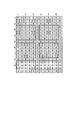
- FIG. 6A is a diagram showing a pixel arrangement before 2 ⁇ 2 pixel mixed readout.
- FIG. 6B is a diagram illustrating a pixel arrangement after 2 ⁇ 2 pixel mixed readout.
- FIG. 7A is a diagram illustrating a pixel arrangement before 3 ⁇ 3 pixel mixed readout.
- FIG. 7B is a diagram illustrating a pixel arrangement after 3 ⁇ 3 pixel mixed readout.
- FIG. 8 is a flowchart showing pixel interpolation processing.
- FIG. 1 is a block diagram illustrating a configuration of a digital camera (hereinafter simply referred to as a camera) as an example of an imaging apparatus according to an embodiment of the present invention.
- a solid line with an arrow indicates a data flow
- a broken line with an arrow indicates a control signal flow.
- the camera 1 shown in FIG. 1 includes a photographic lens 11, an aperture 13, a mechanical shutter 15, a drive unit 17, an operation unit 19, an image sensor 21, an imaging control circuit 23, an A-AMP 25, and analog-digital conversion.
- Unit (ADC) 27, CPU (Central Processing Unit) 29, image processing unit 31, focus detection circuit 33, video encoder 35, display unit 37, bus 39, DRAM (Dynamic Random Access Memory) 41 A ROM (Read Only Memory) 43 and a recording medium 45.
- ADC Central Processing Unit
- CPU Central Processing Unit
- focus detection circuit 33 video encoder 35
- display unit 37 bus 39
- DRAM Dynamic Random Access Memory
- ROM Read Only Memory
- the photographing lens 11 has a single lens or a plurality of lenses for forming an image from the subject 100 on the image sensor 21.
- the taking lens 11 may be a single focus lens or a zoom lens.
- the diaphragm 13 is disposed on the optical axis of the photographic lens 11 and has a variable aperture. The diaphragm 13 limits the amount of light flux from the subject 100 that has passed through the photographing lens 11.
- the mechanical shutter 15 is disposed behind the diaphragm 13 and is configured to be freely opened and closed.
- the mechanical shutter 15 adjusts the incident time of the subject luminous flux from the subject 100 to the image sensor 21 (exposure time of the image sensor 21) by adjusting the opening time.
- a known focal plane shutter, lens shutter, or the like can be employed as the mechanical shutter 15.
- the driving unit 17 performs focus adjustment of the photographing lens 11, aperture diameter control of the diaphragm 13, and opening / closing control of the mechanical shutter 15 based on a control signal from the CPU 29.
- the operation unit 19 includes various operation buttons such as a power button, a release button, a reproduction button, and a menu button, and various operation members such as a touch panel.
- the operation unit 19 detects operation states of various operation members and outputs a signal indicating the detection result to the CPU 29.
- the shooting mode of the camera 1 can be selected by the operation unit 19 of the present embodiment. That is, the user can select the shooting mode of the camera 1 from either the still image shooting mode or the moving image shooting mode by operating a shooting mode dial as an operation member included in the operation unit 19.
- the still image shooting mode is a shooting mode for shooting a still image
- the moving image shooting mode is a shooting mode for shooting a moving image.
- an example in which selection is made with a dial is shown, but the shooting mode may be selected by, for example, operating a touch panel on a menu screen.
- the imaging element 21 is disposed on the optical axis of the photographing lens 11, behind the mechanical shutter 15, and at a position where the subject light beam is imaged by the photographing lens 11.
- the image sensor 21 is configured by two-dimensionally arranging photodiodes that constitute pixels.
- the image sensor 21 in the present embodiment includes an image pickup pixel for acquiring an image for recording and display and a phase difference detection pixel for focus detection.
- the photodiode that constitutes the image sensor 21 generates a charge corresponding to the amount of received light.
- the electric charge generated in the photodiode is accumulated in a capacitor connected to each photodiode.
- the electric charge accumulated in this capacitor is read out as an image signal.
- the image sensor 21 in the present embodiment has a plurality of different charge readout methods.
- the charge accumulated in the image sensor 21 is read according to a control signal from the image capture control circuit 23.
- a Bayer array color filter is disposed on the front surface of the photodiode constituting the pixel.
- the Bayer array has a line in which R pixels and G (Gr) pixels are alternately arranged in the horizontal direction, and a line in which G (Gb) pixels and B pixels are alternately arranged.
- the phase difference detection pixels are arranged at some positions of the imaging pixels. Unlike the other pixels, the pixels used as the phase difference detection pixels shield some areas. Details of the image sensor 21 will be described later.
- the imaging control circuit 23 sets the readout method of the imaging device 21 according to the control signal from the CPU 29, and controls the readout of the image signal from the imaging device 21 according to the set readout method. Details of the imaging control circuit 23 will be described later in detail.
- the A-AMP 25 adjusts the analog gain of the image signal output from the image sensor 21.
- the ADC 27 is an analog-digital converter, and converts the image signal whose analog gain has been adjusted by the A-AMP 25 into a digital image signal (pixel data).
- pixel data a collection of a plurality of pixel data is referred to as imaging data in this specification.
- the CPU 29 performs overall control of the camera 1 according to a program stored in the ROM 43 described later.
- the image processing unit 31 performs various types of image processing on the captured data to generate image data. For example, when recording a still image, the image processing unit 31 performs still image recording image processing to generate still image data. Similarly, when recording a moving image, the image processing unit 31 performs moving image recording image processing to generate moving image data. Furthermore, the image processing unit 31 performs display image processing during live view display to generate display image data. The detailed configuration of the image processing unit 31 will be described in detail later.
- the focus detection circuit 33 acquires pixel data from the phase difference detection pixel, and calculates a defocus direction and a defocus amount with respect to the in-focus position of the photographing lens 11 using a known phase difference method based on the acquired pixel data. To do.
- the video encoder 35 reads the display image data generated by the image processing unit 31 and temporarily stored in the DRAM 41, and outputs the read display image data to the display unit 37.
- the display unit 37 is a display unit such as a liquid crystal display or an organic EL display, and is disposed on the back surface of the camera 1, for example.
- the display unit 37 displays an image according to the display image data input from the video encoder 35.
- the display unit 37 is used for live view display, display of recorded images, and the like.
- the bus 39 is connected to the ADC 27, the CPU 29, the image processing unit 31, the focus detection circuit 33, the video encoder 35, the DRAM 41, the ROM 43, and the recording medium 45. On the bus 39, various data generated in these blocks are transferred.
- the DRAM 41 is an electrically rewritable memory, and temporarily stores various data such as the above-described imaging data (pixel data), recording image data, display image data, and processing data in the CPU 29.
- SDRAM Serial Dynamic Random Access Memory
- the ROM 43 is a non-volatile memory such as a mask ROM or a flash memory.
- the ROM 43 stores various data such as a program used by the CPU 29 and adjustment values of the camera 1.
- the recording medium 45 is configured to be built in or freely loaded in the camera 1 and records recording image data as an image file of a predetermined format.
- FIG. 2 is a diagram illustrating a detailed configuration of the imaging control circuit 23 and the image processing unit 31.
- a solid line with an arrow indicates a flow of imaging data (pixel data).
- a broken line with an arrow indicates a flow of setting data for the imaging control circuit 23
- an alternate long and short dash line with an arrow indicates a flow of RGB data (a result of simultaneous processing of imaging data)
- a two-dot chain line with an arrow indicates YC data ( The flow of RGB data) is represented respectively.
- RGB data or YC data corresponds to the image data described above.
- the imaging control circuit 23 various settings are made according to the readout method of the pixel data from the imaging element 21.
- the imaging control circuit 23 outputs a control signal for reading pixel data from the imaging device 21 to the imaging device 21 in accordance with this setting.
- Such an imaging control circuit 23 includes a readout method setting unit 231 and a mixing rate setting unit 232.
- the readout method of the pixel data from the image sensor 21 is set according to the setting data from the CPU 29.
- the readout method is set according to the operating state of the camera 1. For example, when real-time performance is required for reading pixel data from the image sensor 21 (for example, during live view display or moving image recording), pixel data from a plurality of pixels of the same color is used so that the pixel data can be read at high speed. Are read out, or the pixel data of a specific pixel is read out. On the other hand, when image quality is required rather than real-time characteristics (for example, when recording a still image), resolution is maintained by reading pixel data of all pixels without performing mixed readout or thinning readout.
- the CPU 29 determines the operating state of the camera 1 and generates setting data so that a reading method according to the determined result is obtained.
- the horizontal and vertical pixel reading intervals when the pixel data is mixed or when the pixel data is thinned are set.
- a readout method (2 ⁇ 2 pixel mixed readout) in which a total of 4 pixels are mixed by 2 horizontal and vertical 2 pixels to 1 pixel, or a total of 4 pixels of 2 horizontal and 2 vertical pixels are thinned to 1 pixel.
- the readout method (2 ⁇ 2 pixel thinning readout) is set in the readout method setting unit 231, 2 is set for each of the horizontal readout interval and the vertical readout interval.
- the image processing unit 31 includes a gain adjustment unit 311, an interpolation ratio determination unit 312, a pixel interpolation unit 313, a development processing unit 314, and a color conversion processing unit 315.
- the image processing unit 31 also includes a compression / decompression processing unit and the like.
- the gain adjustment unit 311 performs gain adjustment of pixel data from the phase difference detection pixels. A partial region of the phase difference detection pixel is shielded. For this reason, even when a part of the subject having the same luminance is imaged, the amount of light incident on the phase difference detection pixel is smaller than the amount of light incident on the imaging pixel.
- the gain adjustment unit 311 performs correction to compensate for the dimming of pixel data that occurs by blocking a partial region of the phase difference detection pixel.
- the interpolation ratio determination unit 312 determines the pixel data of the phase difference detection pixel from the mixing rate calculated according to the reading method set in the reading method setting unit 231 and the horizontal / vertical reading interval set in the mixing rate setting unit 232. Determine the application rate.
- the application ratio is a weighting coefficient for weighted addition of the pixel data of the phase difference detection pixel subjected to gain adjustment processing and the pixel data around the phase difference detection pixel. Specifically, in the case of a readout method in which the pixel data mixture rate of the phase difference detection pixel is high, the pixel data of the phase difference detection pixel that has been subjected to gain adjustment processing by increasing the weighting coefficient of the pixel data of the peripheral pixels. Reduce the weighting coefficient.
- the pixel interpolation unit 313 performs a correction process on the pixel data of the phase difference detection pixel based on the application ratio (weighting coefficient) determined by the interpolation ratio determination unit 312.
- the development processing unit 314 performs synchronization processing (demosaicing processing), NR (Noise Reduction) processing, WB (White Balance) correction, edge enhancement processing, and the like on the imaging data including the pixel data interpolated by the pixel interpolation unit 313. Apply.
- synchronization processing demosaicing processing
- NR Noise Reduction
- WB White Balance
- edge enhancement processing edge enhancement processing, and the like on the imaging data including the pixel data interpolated by the pixel interpolation unit 313.
- the color conversion processing unit 315 performs processing for generating display image data or recording image data from the RGB data obtained in the development processing unit 314. This processing includes, for example, processing for converting RGB data into YC data by matrix calculation, gamma correction processing for YC data, and the like.
- FIG. 3 is a diagram illustrating a pixel array of the image sensor 21.
- a part of the pixels is shown in an enlarged manner.
- FIG. 3 shows an example of the Bayer arrangement, but the arrangement of the color filters is not limited to the Bayer arrangement, and various arrangements can be applied.
- the Bayer array image sensor 21 has a line in which R pixels and G (Gr) pixels are alternately arranged in the horizontal direction and a line in which G (Gb) pixels and B pixels are alternately arranged. is doing.
- a set of four pixels of the Gr pixel, the R pixel, the Gb pixel, and the B pixel shown in the enlarged view on the right side is repeatedly arranged in the horizontal and vertical directions.
- phase difference detection pixels are arranged at the positions of some imaging pixels.
- the phase difference detection pixel is, for example, a pixel in which one of the left and right regions is shielded by a light shielding film.
- a row of phase difference detection pixels hereinafter referred to as right opening phase difference detection pixels
- a phase difference detection pixel hereinafter referred to as left opening phase difference detection
- phase difference detection pixels In the case of an image sensor with a large number of pixels, the area of each pixel is small, so it can be considered that the same image is formed on pixels arranged close to each other. Therefore, by arranging the phase difference detection pixels as shown in FIG. 3, the phase difference can be detected by a pair of the phase difference detection pixels in the A row and the B phase difference detection pixels in FIG. The phase difference can also be detected by a pair of phase difference detection pixels in the C row and phase difference detection pixels in the D row.
- the light-shielding region in the phase difference detection pixel is set to either the left or right region. In this case, it is possible to detect the horizontal phase difference. On the other hand, it is also possible to detect a vertical phase difference or a phase difference in an oblique direction by setting a light shielding region as an upper or lower region or an oblique region. Further, as long as it has a certain area, the light shielding area may not be 1/2 of the pixel region. Further, in FIG. 3, the phase difference detection pixel is arranged in the G pixel, but it may be arranged in any of the R pixel and the B pixel other than the G pixel.
- FIG. 3 shows an example in which pupil division is performed by shielding a partial area of the phase difference detection pixel 21b, but the phase difference detection pixel is a pair of pixels that have passed through different pupil areas of the photographing lens 11. It is only necessary to selectively receive one of the subject luminous fluxes forming For this reason, instead of a configuration in which a partial region is shielded from light, for example, pupil division may be performed by a pupil division microlens.
- FIG. 4A shows an imaging state of an image in the imaging pixel 21a.
- FIG. 4B shows an image formation state of the image in the phase difference detection pixel 21b.
- the photographing lens 11 when the photographing lens 11 is in a focused state, a pair of subject luminous fluxes emitted from the subject and passing through different pupil regions symmetric with respect to the optical axis center of the photographing lens 11 are imaged. An image is formed at the same position on the element 21.
- the peak position of the image formed on the imaging pixel 21a matches the peak position of the image formed on the phase difference detection pixel 21b.
- a part of the region of the phase difference detection pixel 21b is shielded from light, only the peak of one image of a pair of subject light beams is detected. For this reason, a decrease in the amount of light occurs in the phase difference detection pixel 21b.
- a pair of subject luminous fluxes emitted from the subject and passing through different pupil regions of the photographing lens 11 form images at different positions on the image sensor 21.
- an image corresponding to each of the subject luminous fluxes that have passed through different pupil regions is formed on the imaging pixel 21a.
- only an image corresponding to one of the subject luminous fluxes passing through different pupil regions is formed on the phase difference detection pixel 21b.
- the peak position of the image formed on the imaging pixel 21a and the peak position of the image formed on the phase difference detection pixel 21b do not coincide with each other, and an image shift occurs.
- the amount of light also decreases.
- FIG. 5 is a flowchart showing the process of moving image recording (moving image shooting) operation by the imaging apparatus.
- the moving image recording operation is started, for example, when the release button is pressed during the moving image shooting mode. 5 is executed by the CPU 29 according to a program stored in the ROM 43. Note that FIG. 5 shows the operation at the time of moving image recording, but the imaging control method of the present embodiment described below can also be applied at the time of still image recording or live view display.
- the CPU 29 starts taking in the imaging data (step S101).
- the CPU 29 inputs setting data corresponding to the current operation mode to the reading method setting unit 231 of the imaging control circuit 23.
- the imaging control circuit 23 controls reading of pixel data from the imaging element 21.
- the setting data corresponding to the readout method at the time of moving image recording is input.
- the mixing rate setting unit 232 sets the horizontal and vertical pixel reading intervals when mixing or thinning out pixel data. For example, in the case of 2 ⁇ 2 pixel mixed readout or 2 ⁇ 2 pixel thinning readout, 2 is set for each of the horizontal readout interval and the vertical readout interval. In the case of 3 ⁇ 3 pixel mixed readout or 3 ⁇ 3 pixel thinning readout, 3 is set for each of the horizontal readout interval and the vertical readout interval.
- an image signal in a state of pixel mixture or pixel thinning is read out from the imaging device 21 in accordance with the readout method set in the imaging control circuit 23.
- the image signal read from the image sensor 21 is digitized by the ADC 27 and then temporarily stored in the DRAM 41 as image data.
- the CPU 29 performs focus detection processing (step S102).
- the CPU 29 causes the focus detection circuit 33 to execute focus detection processing.
- the focus detection circuit 33 reads out pixel data corresponding to the phase difference detection pixel (mixed or thinned out) from the imaging data temporarily stored in the DRAM 41, and uses this pixel data as the pixel data.
- the defocus direction and defocus amount of the photographic lens 11 are calculated using a known phase difference method.
- the CPU 29 performs a mixing rate calculation process (step S103).
- the CPU 29 calculates the mixing rate, which is a value necessary for the interpolation rate determination unit 312 to determine the interpolation rate.
- the mixing rate is the mixing rate of the pixel data of the phase difference detection pixel in each pixel data after the pixel mixture reading or the pixel thinning-out reading.
- FIG. 6A is a diagram showing a pixel arrangement before 2 ⁇ 2 pixel mixed readout.
- FIG. 6B is a diagram showing a pixel arrangement after 2 ⁇ 2 pixel mixed readout.
- the numbers attached to the upper side and the left side of FIGS. 6A and 6B indicate the coordinates of the pixel. In the following description, it is assumed that two horizontal and vertical pixels including R pixels with numbers are the same coordinates.
- r shown in FIG. 6A indicates a phase difference detection pixel (right opening phase difference detection pixel) whose left half surface is shielded
- l shown in FIG. 6A is a phase difference detection pixel (left) whose right half surface is shielded.
- r shown in the left diagram of FIG. 6B indicates that the right aperture phase difference detection pixel is mixed in that pixel
- l shown in the left diagram of FIG. 6B indicates that the left aperture phase difference detection is detected in that pixel. Indicates that a pixel is mixed.
- the numbers attached to r and l in FIG. 6B indicate the number of right aperture phase difference detection pixels or left aperture phase difference detection pixels mixed in the pixels. Furthermore, the numbers shown on the right side of FIG. 6B indicate the total number of phase difference detection pixels mixed in each pixel.
- FIG. Pixel data of the R pixel at the coordinates (1, 1) is obtained.
- Other colors other than the R pixel are mixed in the same manner.
- the phase difference detection pixel is arranged at the position of the G (Gb) pixel
- the pixel data of the phase difference detection pixel is mixed into the pixel data after addition.
- the pixel data in the thick frame in FIG. 6A are mixed, the pixel data of the phase difference detection pixel is mixed.
- phase difference detection pixel in the case of 2 ⁇ 2 pixel mixed readout, pixel data of each phase difference detection pixel is mixed into the pixel data at each Gb position after mixing.
- a pixel mixed with pixel data of such a phase difference detection pixel can be used as a phase difference detection pixel even after mixed reading.
- FIG. 7A is a diagram showing pixel data before 3 ⁇ 3 pixel mixed readout.
- FIG. 7B is a diagram showing pixel data after 3 ⁇ 3 pixel mixed readout.
- pixel data of the same color for each horizontal and vertical pixel is mixed.
- the coordinates (2, 1), coordinates (2, 2), coordinates (2, 3), coordinates (3, 1), (3, 2), (3, 3), (4, 1) shown in FIG. ), (4, 2), and (4, 3) of the nine R pixel data are mixed to obtain the pixel data of the R pixel at the coordinates (1, 1) in FIG. 7B.
- Other colors other than the R pixel are mixed in the same manner.
- the pixel data of the first row is not used for mixing, but the pixel data of the first row may be used for mixing.
- the phase difference detection pixel is arranged at the position of the G (Gb) pixel
- the pixel data of the phase difference detection pixel is mixed into the pixel data after addition. Is done. That is, when the pixel data in the thick frame in FIG. 7A are mixed, the pixel data of the phase difference detection pixel is mixed.
- FIG. 7B in the case of 3 ⁇ 3 pixel mixed readout, the number of pixel data of the phase difference detection pixels mixed depending on the position is different.
- the number of pixel data of the phase difference detection pixels included in the pixel data after readout is n
- the horizontal readout interval at the time of pixel mixing or pixel decimation is h
- the vertical readout interval at the time of pixel mixing or pixel decimation is calculated for each pixel position according to the following (Equation 1).
- ⁇ n / (h ⁇ v) (Formula 1)
- ⁇ is 1 ⁇ 4 regardless of the position of the Gb pixel.
- ⁇ 3 ⁇ 3 pixel mixed readout ⁇ changes between 1/9 and 4/9 according to the position of the Gb pixel.
- the above example shows an example in which the mixing rate is calculated for each moving image recording, but the mixing rate for each reading method may be calculated in advance. In this case, it is only necessary to acquire the corresponding mixing rate when the reading method is set.
- the CPU 29 performs gain adjustment processing (step S104).
- the CPU 29 causes the gain adjustment unit 311 of the image processing unit 31 to perform gain adjustment.
- the gain adjustment amount is determined in consideration of the pixel data mixing rate of the phase difference detection pixels. In order to simplify the description, assuming that the amount of light is 1/2 in a phase difference detection pixel that shields either the left or right region as shown in FIG. 3, the gain adjustment amount ⁇ is given by the following (formula 2). .
- ⁇ (h ⁇ v) / ((h ⁇ v) ⁇ n ⁇ 0.5) (Formula 2)
- ⁇ is 4 / 3.5 regardless of the position of the Gb pixel.
- ⁇ changes between 9 / 8.5 and 9/7 depending on the position of the Gb pixel.
- the specific process of the gain adjustment process is a process of multiplying the value of the pixel data of the phase difference detection pixel by the gain adjustment amount ⁇ obtained by (Equation 2).
- Equation 2 assumes that the amount of light in the phase difference detection pixel is 1/2. Actually, the amount of light reduction varies depending on the aperture of the taking lens 11, the aperture of the diaphragm 13, and the like. Therefore, it is desirable that 0.5 in (Equation 2) is adaptively switched according to the aperture of the taking lens 11, the aperture of the diaphragm 13, and the like.
- the CPU 29 performs pixel interpolation processing (step S105).
- the CPU 29 causes the interpolation ratio determination unit 312 and the pixel interpolation unit 313 of the image processing unit 31 to perform pixel interpolation processing.
- the pixel interpolation process will be described in detail later.
- the CPU 29 performs lens driving (step S106).
- the CPU 29 controls the drive unit 17 based on the defocus direction and the defocus amount of the photographing lens 11 detected by the focus detection circuit 33 in step S102, and focuses the photographing lens 11.
- the CPU 29 performs image processing (step S107).
- the CPU 29 causes the development processing unit 314 and the color conversion processing unit 315 of the image processing unit 31 to execute the development processing and color conversion processing on the imaging data temporarily stored in the DRAM 41 as a result of the pixel interpolation processing in step S105.
- Processing parameters used for development processing and color conversion processing are those for recording.
- the processing parameters for recording are stored in advance in the ROM 43, for example.
- the CPU 29 records the image data temporarily stored in the DRAM 41 as a result of the image processing on the recording medium 45 (step S108).
- the CPU 29 determines whether or not to stop moving image recording (step S109).
- the CPU 29 determines the operation state of the release button of the operation unit 19. That is, when the release button is pressed again, the CPU 29 determines to stop moving image recording.
- step S109 When it is determined in step S109 that the moving image recording is not stopped, the CPU 29 returns the process to step S101 and continues the moving image recording. On the other hand, when it is determined in step S109 that the moving image recording is to be stopped, the CPU 29 ends the process of FIG.
- FIG. 8 is a flowchart showing details of pixel interpolation processing.
- the pixel interpolation process is a process performed mainly by the interpolation ratio determination unit 312 and the pixel interpolation unit 313.
- the interpolation ratio determination unit 312 determines whether or not pixel data of the phase difference detection pixel is included in the imaging data to be processed (step S201).
- the coordinate data of the phase difference detection pixel is stored in advance in the ROM 43, for example, and the interpolation ratio determination unit 312 determines whether or not the pixel data of the phase difference detection pixel is included in the imaging data to be processed from this coordinate data. judge.
- whether or not the pixel data of the phase difference detection pixel is included in the pixel data after reading is also determined by the reading method.
- the interpolation ratio determination unit 312 acquires the setting data of the readout method setting unit 231 and the mixing rate setting unit 232, refers to the coordinate data of the phase difference detection pixels according to the acquired setting data, and sets the imaging data. It is determined whether or not pixel data of the phase difference detection pixel is included.
- step S201 If it is determined in step S201 that the pixel data of the phase difference detection pixel is not included in the imaging data to be processed, the processing in FIG. 8 is terminated.
- step S201 when it is determined that the imaging data to be processed includes the pixel data of the phase difference detection pixel, the interpolation ratio determination unit 312 determines the mixing rate ⁇ calculated by the above-described mixing rate calculation process. Is acquired (step S202).
- correct_pixel af_pixel_weight ⁇ af_pixel + near_pixel_weight ⁇ (pixel_h_1 + pixel_h_2 + pixel_v_1 + pixel_v_2) (Formula 4) “Correct_pixel” in (Expression 4) indicates the value of the corrected pixel data after weighted addition. Further, af_pixel indicates the value of pixel data of the phase difference detection pixel (actually pixel data of the pixel including the phase difference detection pixel). Pixel_h_1 indicates the value of pixel data of the same color pixel of the left + 1 pixel of the phase difference detection pixel (pixel data on the upper left in the case of the Bayer array).
- Pixel_h_2 indicates the value of the pixel data of the same color pixel of the right + 1 pixel of the phase difference detection pixel (pixel data on the lower right in the case of the Bayer array).
- pixel_v_1 indicates the value of pixel data of the same color pixel of the upper +1 pixel of the phase difference detection pixel (pixel data on the upper right in the case of the Bayer array).
- pixel_v_2 indicates the value of pixel data of the same color pixel of the lower +1 pixel of the phase difference detection pixel (pixel data on the lower left in the case of the Bayer array).
- Equation 4 The weighted addition shown in (Equation 4) is performed for each phase difference detection pixel. After the weighted addition shown in (Equation 4) is performed for all the phase difference detection pixels, the processing in FIG. 8 ends.
- the present embodiment when pixel mixing or pixel thinning is performed, according to the mixing ratio of the pixel data of the phase difference detection pixel in each phase difference detection pixel after pixel mixing or after pixel thinning, The application ratio between the pixel data of each phase difference detection pixel and the interpolation data from the surrounding pixel data is changed.
- the pixel data mixture rate of the phase difference detection pixel is low, the application ratio of the pixel data of the phase difference detection pixel after gain adjustment is high, so that overcorrection does not occur and the sharpness of the image is reduced. Can be suppressed.
- the pixel data mixture rate of the phase difference detection pixel is high, the application ratio of the pixel data of the peripheral pixels is high, so that it is possible to suppress the influence of image shift caused by using the phase difference detection pixel. It is.
- each process according to the above-described embodiment can be stored as a program that can be executed by the CPU 29.
- memory cards ROM cards, RAM cards, etc.
- magnetic disks floppy disks, hard disks, etc.
- optical disks CD-ROM, DVD, etc.
- storage media of external storage devices such as semiconductor memories, etc. are distributed. be able to.
- the CPU 29 can execute the above-described processing by reading a program stored in the storage medium of the external storage device and controlling the operation by the read program.
- the above-described embodiments include inventions at various stages, and various inventions can be extracted by appropriately combining a plurality of disclosed constituent elements. For example, even if some configuration requirements are deleted from all the configuration requirements shown in the embodiment, the above-described problem can be solved, and this configuration requirement is deleted when the above-described effects can be obtained.
- the configuration can also be extracted as an invention.
Landscapes
- Engineering & Computer Science (AREA)
- Multimedia (AREA)
- Signal Processing (AREA)
- Physics & Mathematics (AREA)
- General Physics & Mathematics (AREA)
- Optics & Photonics (AREA)
- Spectroscopy & Molecular Physics (AREA)
- Studio Devices (AREA)
- Automatic Focus Adjustment (AREA)
- Focusing (AREA)
- Transforming Light Signals Into Electric Signals (AREA)
Abstract
L'invention concerne un dispositif d'imagerie comprenant un élément d'imagerie (21), une unité de définition de schéma de lecture (231), et une unité de traitement d'image (31). Aux positions de certains pixels d'imagerie de l'élément d'imagerie (21), des pixels de détection de différence de phase pour détecter une mise au point sont disposés. L'unité de définition de schéma de lecture (231) définit le schéma de lecture de données de pixels lues parmi les pixels de détection de différence de phase et les pixels d'imagerie de l'élément d'imagerie (21). L'unité de traitement d'image (31) exécute un traitement pour corriger les données de pixels provenant des pixels de détection de différence de phase. Lorsque le traitement de correction est effectué, l'unité de traitement d'image (31) effectue un traitement de correction de telle sorte le rapport d'application de données de pixels de lecture pour les pixels de détection de différence de phase par rapport à des données d'interpolation obtenues à partir de données de pixels proches des pixels de détection de différence de phase est modifié en fonction du schéma de lecture définit par l'unité de définition de schéma de lecture
Priority Applications (4)
| Application Number | Priority Date | Filing Date | Title |
|---|---|---|---|
| EP13803935.9A EP2863626B1 (fr) | 2012-06-14 | 2013-06-12 | Dispositif d'imagerie et procédé de commande pour dispositif d'imagerie |
| CN201380024415.6A CN104285436B (zh) | 2012-06-14 | 2013-06-12 | 摄像装置和摄像装置的控制方法 |
| US14/535,008 US9167181B2 (en) | 2012-06-14 | 2014-11-06 | Imaging apparatus and method for controlling the imaging apparatus |
| US14/857,115 US9451160B2 (en) | 2012-06-14 | 2015-09-17 | Imaging apparatus and method for controlling the imaging apparatus |
Applications Claiming Priority (2)
| Application Number | Priority Date | Filing Date | Title |
|---|---|---|---|
| JP2012134730A JP5529928B2 (ja) | 2012-06-14 | 2012-06-14 | 撮像装置及び撮像装置の制御方法 |
| JP2012-134730 | 2012-06-14 |
Related Child Applications (1)
| Application Number | Title | Priority Date | Filing Date |
|---|---|---|---|
| US14/535,008 Continuation US9167181B2 (en) | 2012-06-14 | 2014-11-06 | Imaging apparatus and method for controlling the imaging apparatus |
Publications (1)
| Publication Number | Publication Date |
|---|---|
| WO2013187447A1 true WO2013187447A1 (fr) | 2013-12-19 |
Family
ID=49758265
Family Applications (1)
| Application Number | Title | Priority Date | Filing Date |
|---|---|---|---|
| PCT/JP2013/066245 Ceased WO2013187447A1 (fr) | 2012-06-14 | 2013-06-12 | Dispositif d'imagerie et procédé de commande pour dispositif d'imagerie |
Country Status (5)
| Country | Link |
|---|---|
| US (2) | US9167181B2 (fr) |
| EP (1) | EP2863626B1 (fr) |
| JP (1) | JP5529928B2 (fr) |
| CN (1) | CN104285436B (fr) |
| WO (1) | WO2013187447A1 (fr) |
Cited By (3)
| Publication number | Priority date | Publication date | Assignee | Title |
|---|---|---|---|---|
| WO2015186411A1 (fr) * | 2014-06-05 | 2015-12-10 | オリンパス株式会社 | Dispositif d'imagerie et procédé d'imagerie |
| CN105187738A (zh) * | 2014-06-18 | 2015-12-23 | 奥林巴斯株式会社 | 摄像元件、摄像装置 |
| WO2016140066A1 (fr) * | 2015-03-02 | 2016-09-09 | ソニー株式会社 | Dispositif de traitement de signal, procédé de traitement de signal, programme, dispositif électronique et élément d'imagerie |
Families Citing this family (14)
| Publication number | Priority date | Publication date | Assignee | Title |
|---|---|---|---|---|
| JP5747124B2 (ja) * | 2012-06-01 | 2015-07-08 | 富士フイルム株式会社 | 撮像装置 |
| WO2014046037A1 (fr) * | 2012-09-19 | 2014-03-27 | 富士フイルム株式会社 | Dispositif de formation d'image et procédé destiné à le commander |
| JP5775976B2 (ja) * | 2012-11-22 | 2015-09-09 | 富士フイルム株式会社 | 撮像装置、デフォーカス量演算方法、及び撮像光学系 |
| WO2014098143A1 (fr) * | 2012-12-18 | 2014-06-26 | 富士フイルム株式会社 | Dispositif de traitement d'images, dispositif d'imagerie, procédé de traitement d'images, et programme de traitement d'images |
| US9826174B2 (en) * | 2013-03-26 | 2017-11-21 | Samsung Electronics Co., Ltd | Image processing apparatus and method |
| JP6466656B2 (ja) | 2014-06-19 | 2019-02-06 | オリンパス株式会社 | 撮像素子および撮像装置 |
| JP6463010B2 (ja) | 2014-06-24 | 2019-01-30 | オリンパス株式会社 | 撮像素子および撮像装置 |
| JP6364259B2 (ja) * | 2014-07-02 | 2018-07-25 | オリンパス株式会社 | 撮像装置、画像処理方法、及び画像処理プログラム |
| TWI558211B (zh) * | 2015-11-19 | 2016-11-11 | 晶相光電股份有限公司 | 影像處理方法與裝置 |
| JP6427720B2 (ja) * | 2016-06-01 | 2018-11-21 | 富士フイルム株式会社 | 撮像素子及び撮像装置 |
| JP6765953B2 (ja) * | 2016-12-22 | 2020-10-07 | キヤノン株式会社 | 撮像装置及びその制御方法 |
| US10567636B2 (en) * | 2017-08-07 | 2020-02-18 | Qualcomm Incorporated | Resolution enhancement using sensor with plural photodiodes per microlens |
| DE102019128781A1 (de) | 2019-10-24 | 2021-04-29 | Leica Camera Aktiengesellschaft | Verfahren zur Erzeugung eines Ausgabesignals eines PDAF-Bildpunkts |
| KR20220036630A (ko) | 2020-09-16 | 2022-03-23 | 삼성전자주식회사 | 컬러 보정을 위한 영상 처리 장치, 영상 처리 방법 및 이를 포함하는 영상 처리 시스템 |
Citations (9)
| Publication number | Priority date | Publication date | Assignee | Title |
|---|---|---|---|---|
| JP3592147B2 (ja) | 1998-08-20 | 2004-11-24 | キヤノン株式会社 | 固体撮像装置 |
| JP2007279597A (ja) * | 2006-04-11 | 2007-10-25 | Nikon Corp | 撮像装置、カメラおよび画像処理方法 |
| JP2010062640A (ja) | 2008-09-01 | 2010-03-18 | Canon Inc | 撮像装置、撮像装置の制御方法及びプログラム |
| JP2010181751A (ja) * | 2009-02-06 | 2010-08-19 | Canon Inc | 自動焦点検出装置 |
| JP2010271670A (ja) * | 2009-05-25 | 2010-12-02 | Canon Inc | 撮像装置 |
| JP2011081271A (ja) * | 2009-10-08 | 2011-04-21 | Canon Inc | 撮像装置 |
| JP2011199493A (ja) * | 2010-03-18 | 2011-10-06 | Nikon Corp | カメラ |
| JP2011244288A (ja) * | 2010-05-19 | 2011-12-01 | Fujifilm Corp | 撮像装置及び撮像画像信号の補正方法 |
| JP2012088617A (ja) * | 2010-10-21 | 2012-05-10 | Olympus Corp | 撮像装置 |
Family Cites Families (5)
| Publication number | Priority date | Publication date | Assignee | Title |
|---|---|---|---|---|
| EP2179581B1 (fr) * | 2007-08-10 | 2015-11-11 | Canon Kabushiki Kaisha | Appareil de capture d'image et son procédé de commande |
| JP5092685B2 (ja) * | 2007-10-23 | 2012-12-05 | 株式会社ニコン | 撮像素子および撮像装置 |
| JP5595014B2 (ja) * | 2009-11-09 | 2014-09-24 | キヤノン株式会社 | 撮像装置 |
| JP5453173B2 (ja) * | 2010-05-28 | 2014-03-26 | 富士フイルム株式会社 | 撮像装置及び位相差検出画素を持つ固体撮像素子並びに撮像装置の駆動制御方法 |
| JP5853594B2 (ja) * | 2011-10-31 | 2016-02-09 | ソニー株式会社 | 情報処理装置、情報処理方法およびプログラム |
-
2012
- 2012-06-14 JP JP2012134730A patent/JP5529928B2/ja not_active Expired - Fee Related
-
2013
- 2013-06-12 EP EP13803935.9A patent/EP2863626B1/fr not_active Not-in-force
- 2013-06-12 WO PCT/JP2013/066245 patent/WO2013187447A1/fr not_active Ceased
- 2013-06-12 CN CN201380024415.6A patent/CN104285436B/zh not_active Expired - Fee Related
-
2014
- 2014-11-06 US US14/535,008 patent/US9167181B2/en not_active Expired - Fee Related
-
2015
- 2015-09-17 US US14/857,115 patent/US9451160B2/en not_active Expired - Fee Related
Patent Citations (9)
| Publication number | Priority date | Publication date | Assignee | Title |
|---|---|---|---|---|
| JP3592147B2 (ja) | 1998-08-20 | 2004-11-24 | キヤノン株式会社 | 固体撮像装置 |
| JP2007279597A (ja) * | 2006-04-11 | 2007-10-25 | Nikon Corp | 撮像装置、カメラおよび画像処理方法 |
| JP2010062640A (ja) | 2008-09-01 | 2010-03-18 | Canon Inc | 撮像装置、撮像装置の制御方法及びプログラム |
| JP2010181751A (ja) * | 2009-02-06 | 2010-08-19 | Canon Inc | 自動焦点検出装置 |
| JP2010271670A (ja) * | 2009-05-25 | 2010-12-02 | Canon Inc | 撮像装置 |
| JP2011081271A (ja) * | 2009-10-08 | 2011-04-21 | Canon Inc | 撮像装置 |
| JP2011199493A (ja) * | 2010-03-18 | 2011-10-06 | Nikon Corp | カメラ |
| JP2011244288A (ja) * | 2010-05-19 | 2011-12-01 | Fujifilm Corp | 撮像装置及び撮像画像信号の補正方法 |
| JP2012088617A (ja) * | 2010-10-21 | 2012-05-10 | Olympus Corp | 撮像装置 |
Non-Patent Citations (1)
| Title |
|---|
| See also references of EP2863626A4 |
Cited By (5)
| Publication number | Priority date | Publication date | Assignee | Title |
|---|---|---|---|---|
| WO2015186411A1 (fr) * | 2014-06-05 | 2015-12-10 | オリンパス株式会社 | Dispositif d'imagerie et procédé d'imagerie |
| JP2015230385A (ja) * | 2014-06-05 | 2015-12-21 | オリンパス株式会社 | 撮像装置および撮像方法 |
| CN105187738A (zh) * | 2014-06-18 | 2015-12-23 | 奥林巴斯株式会社 | 摄像元件、摄像装置 |
| CN105187738B (zh) * | 2014-06-18 | 2019-03-19 | 奥林巴斯株式会社 | 摄像元件、摄像装置 |
| WO2016140066A1 (fr) * | 2015-03-02 | 2016-09-09 | ソニー株式会社 | Dispositif de traitement de signal, procédé de traitement de signal, programme, dispositif électronique et élément d'imagerie |
Also Published As
| Publication number | Publication date |
|---|---|
| US9167181B2 (en) | 2015-10-20 |
| EP2863626A4 (fr) | 2015-11-25 |
| US20150062374A1 (en) | 2015-03-05 |
| JP5529928B2 (ja) | 2014-06-25 |
| CN104285436A (zh) | 2015-01-14 |
| EP2863626B1 (fr) | 2017-03-08 |
| JP2013257494A (ja) | 2013-12-26 |
| US20160006931A1 (en) | 2016-01-07 |
| EP2863626A1 (fr) | 2015-04-22 |
| US9451160B2 (en) | 2016-09-20 |
| CN104285436B (zh) | 2017-09-22 |
Similar Documents
| Publication | Publication Date | Title |
|---|---|---|
| JP5529928B2 (ja) | 撮像装置及び撮像装置の制御方法 | |
| JP5888940B2 (ja) | 撮像装置、撮像装置の制御方法、およびプログラム | |
| US9843735B2 (en) | Image processing apparatus, imaging apparatus comprising the same, and image processing method | |
| JP6021622B2 (ja) | 画像処理装置及び画像処理方法 | |
| JP6099536B2 (ja) | 画像処理装置、画像処理方法及び画像処理プログラム | |
| JP5826901B2 (ja) | 撮像装置及び光軸位置算出方法 | |
| US9503661B2 (en) | Imaging apparatus and image processing method | |
| JP5701942B2 (ja) | 撮像装置、カメラシステム及び画像処理方法 | |
| JP6270400B2 (ja) | 画像処理装置、画像処理方法及び画像処理プログラム | |
| JP6364259B2 (ja) | 撮像装置、画像処理方法、及び画像処理プログラム | |
| JP5792349B2 (ja) | 撮像装置及び撮像装置の制御方法 | |
| JP6017641B1 (ja) | 撮像装置,信号処理方法,信号処理プログラム | |
| JP6184132B2 (ja) | 撮像装置および画像処理方法 | |
| WO2015182021A1 (fr) | Appareil et procédé de commande de capture d'image et appareil de capture d'image |
Legal Events
| Date | Code | Title | Description |
|---|---|---|---|
| 121 | Ep: the epo has been informed by wipo that ep was designated in this application |
Ref document number: 13803935 Country of ref document: EP Kind code of ref document: A1 |
|
| NENP | Non-entry into the national phase |
Ref country code: DE |
|
| REEP | Request for entry into the european phase |
Ref document number: 2013803935 Country of ref document: EP |
|
| WWE | Wipo information: entry into national phase |
Ref document number: 2013803935 Country of ref document: EP |