WO2013190609A1 - Système d'onduleur et procédé de communication - Google Patents
Système d'onduleur et procédé de communication Download PDFInfo
- Publication number
- WO2013190609A1 WO2013190609A1 PCT/JP2012/065475 JP2012065475W WO2013190609A1 WO 2013190609 A1 WO2013190609 A1 WO 2013190609A1 JP 2012065475 W JP2012065475 W JP 2012065475W WO 2013190609 A1 WO2013190609 A1 WO 2013190609A1
- Authority
- WO
- WIPO (PCT)
- Prior art keywords
- inverter
- data
- slave
- pwm carrier
- motor
- Prior art date
- Legal status (The legal status is an assumption and is not a legal conclusion. Google has not performed a legal analysis and makes no representation as to the accuracy of the status listed.)
- Ceased
Links
Images





Classifications
-
- H—ELECTRICITY
- H02—GENERATION; CONVERSION OR DISTRIBUTION OF ELECTRIC POWER
- H02M—APPARATUS FOR CONVERSION BETWEEN AC AND AC, BETWEEN AC AND DC, OR BETWEEN DC AND DC, AND FOR USE WITH MAINS OR SIMILAR POWER SUPPLY SYSTEMS; CONVERSION OF DC OR AC INPUT POWER INTO SURGE OUTPUT POWER; CONTROL OR REGULATION THEREOF
- H02M7/00—Conversion of AC power input into DC power output; Conversion of DC power input into AC power output
- H02M7/42—Conversion of DC power input into AC power output without possibility of reversal
-
- H—ELECTRICITY
- H02—GENERATION; CONVERSION OR DISTRIBUTION OF ELECTRIC POWER
- H02P—CONTROL OR REGULATION OF ELECTRIC MOTORS, ELECTRIC GENERATORS OR DYNAMO-ELECTRIC CONVERTERS; CONTROLLING TRANSFORMERS, REACTORS OR CHOKE COILS
- H02P27/00—Arrangements or methods for the control of AC motors characterised by the kind of supply voltage
- H02P27/04—Arrangements or methods for the control of AC motors characterised by the kind of supply voltage using variable-frequency supply voltage, e.g. inverter or converter supply voltage
- H02P27/06—Arrangements or methods for the control of AC motors characterised by the kind of supply voltage using variable-frequency supply voltage, e.g. inverter or converter supply voltage using DC to AC converters or inverters
- H02P27/08—Arrangements or methods for the control of AC motors characterised by the kind of supply voltage using variable-frequency supply voltage, e.g. inverter or converter supply voltage using DC to AC converters or inverters with pulse width modulation
-
- H—ELECTRICITY
- H02—GENERATION; CONVERSION OR DISTRIBUTION OF ELECTRIC POWER
- H02M—APPARATUS FOR CONVERSION BETWEEN AC AND AC, BETWEEN AC AND DC, OR BETWEEN DC AND DC, AND FOR USE WITH MAINS OR SIMILAR POWER SUPPLY SYSTEMS; CONVERSION OF DC OR AC INPUT POWER INTO SURGE OUTPUT POWER; CONTROL OR REGULATION THEREOF
- H02M1/00—Details of apparatus for conversion
- H02M1/08—Circuits specially adapted for the generation of control voltages for semiconductor devices incorporated in static converters
-
- H—ELECTRICITY
- H02—GENERATION; CONVERSION OR DISTRIBUTION OF ELECTRIC POWER
- H02M—APPARATUS FOR CONVERSION BETWEEN AC AND AC, BETWEEN AC AND DC, OR BETWEEN DC AND DC, AND FOR USE WITH MAINS OR SIMILAR POWER SUPPLY SYSTEMS; CONVERSION OF DC OR AC INPUT POWER INTO SURGE OUTPUT POWER; CONTROL OR REGULATION THEREOF
- H02M7/00—Conversion of AC power input into DC power output; Conversion of DC power input into AC power output
- H02M7/42—Conversion of DC power input into AC power output without possibility of reversal
- H02M7/44—Conversion of DC power input into AC power output without possibility of reversal by static converters
- H02M7/48—Conversion of DC power input into AC power output without possibility of reversal by static converters using discharge tubes with control electrode or semiconductor devices with control electrode
- H02M7/493—Conversion of DC power input into AC power output without possibility of reversal by static converters using discharge tubes with control electrode or semiconductor devices with control electrode the static converters being arranged for operation in parallel
-
- H—ELECTRICITY
- H02—GENERATION; CONVERSION OR DISTRIBUTION OF ELECTRIC POWER
- H02P—CONTROL OR REGULATION OF ELECTRIC MOTORS, ELECTRIC GENERATORS OR DYNAMO-ELECTRIC CONVERTERS; CONTROLLING TRANSFORMERS, REACTORS OR CHOKE COILS
- H02P27/00—Arrangements or methods for the control of AC motors characterised by the kind of supply voltage
- H02P27/04—Arrangements or methods for the control of AC motors characterised by the kind of supply voltage using variable-frequency supply voltage, e.g. inverter or converter supply voltage
- H02P27/06—Arrangements or methods for the control of AC motors characterised by the kind of supply voltage using variable-frequency supply voltage, e.g. inverter or converter supply voltage using DC to AC converters or inverters
Definitions
- the present invention relates to an inverter system and a communication method.
- Patent Document 1 in a serial communication device for motor control in which a host control device and a plurality of motor drive devices are connected in a daisy chain, communication timing counters having the same count-up speed are provided inside all the motor drive devices, and the host control It is described that when command data is transmitted from the apparatus to all the motor drive devices, the communication timing counter is reset at the timing when the command data is normally taken in all the motor drive devices.
- the communication timing counter since all the motor drive devices can simultaneously reflect the command data in the control and sample the feedback data based on the communication timing counter, a plurality of motors can operate in a coordinated manner. In this case, the operation of each motor is not deviated and it is supposed that highly accurate control is possible.
- Patent Document 1 The technique described in Patent Document 1 is based on the premise that a plurality of motor driving devices drive different motors. That is, in the technique described in Patent Document 1, it is considered that a plurality of connections between a plurality of motor driving devices and a plurality of motors are independent from each other.
- the master inverter and one or more slave inverters are connected in parallel to one motor via a common connection node
- the master inverter and one or more slave inverters are connected to each other via a common connection node.
- a cross current may flow between the master inverter and one or more slave inverters.
- the present invention has been made in view of the above, and an object thereof is to obtain an inverter system and a communication method capable of suppressing a cross current between a master inverter and one or more slave inverters.
- an inverter system is connected to a master inverter connected to a motor and the master inverter via a half-duplex communication line. And at least one slave inverter connected to the motor in parallel with the master inverter via a common connection node, wherein the master inverter is connected to a first PWM carrier and a first command voltage.
- Each of the one or more slave inverters drives the motor based on a second PWM carrier and a second command voltage.
- the drive unit receives the first data via the half-duplex communication line, and synchronizes with the second PWM carrier at a timing that avoids the reception timing of the first data from the slave inverter.
- a communication unit that broadcast-transmits the second data including the actual output current to the motor to the half-duplex communication line, and matches the phase of the first PWM carrier according to the reception timing of the first data
- a phase adjustment unit that adjusts the phase of the second PWM carrier, and the master inverter receives the second data received when the second data is received by the communication unit.
- the actual output current from the master inverter to the motor and the actual output current from each of the one or more slave inverters to the motor As it is balanced, characterized by further comprising an amplitude adjusting section for adjusting an amplitude of the first command voltage.
- the phase of the second PWM carrier is adjusted so as to match the phase of the first PWM carrier, the phase shift between the first PWM carrier and the second PWM carrier is reduced. it can. Further, since the amplitude of the first command voltage is adjusted so that the actual output current from the master inverter to the motor and the actual output current from the slave inverter to the motor are balanced, the first command voltage and the second command voltage are adjusted. Amplitude deviation from the command voltage can be reduced. Thereby, the cross current between the master inverter and one or more slave inverters can be suppressed.
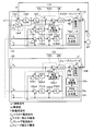
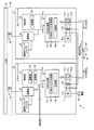
- FIG. 1 is a diagram illustrating a configuration of the inverter system according to the first embodiment.
- FIG. 2 is a diagram illustrating a configuration of the inverter system according to the first embodiment.
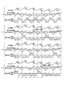
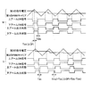
- FIG. 3 is a diagram illustrating an operation of the inverter system according to the first embodiment.
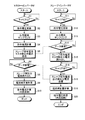
- FIG. 4 is a flowchart of the operation of the inverter system according to the first embodiment.
- FIG. 5 is a diagram of a configuration of the inverter system according to the second embodiment.
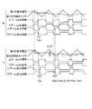
- FIG. 6 is a diagram illustrating an operation of the inverter system according to the second embodiment.
- FIG. 7 is a diagram illustrating an operation of the inverter system according to the second embodiment.
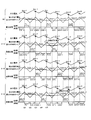
- FIG. 8 is a diagram illustrating the operation of the inverter system according to the third embodiment.
- FIG. 9 is a diagram showing a configuration of an inverter system according to a basic form.
- FIG. 10 is a diagram illustrating the operation of the inverter system according to the basic mode.
- FIG. 11 is a diagram illustrating the operation of the inverter system according to the basic mode.
- FIG. 12 is a diagram illustrating a configuration of an inverter system according to a modification of the basic mode.
- FIG. 9 is a diagram showing a configuration of the inverter system 1 according to the basic mode.
- One motor is generally driven by one inverter, but when the capacity of the motor is larger than the capacity of the inverter, for example, when the capacity of the motor is 800 kW and the capacity of one inverter is 500 kW, It is difficult for one inverter to properly drive one motor according to a predetermined command.
- a parallel drive system in which outputs of a plurality of inverters are connected in parallel can be considered.
- the capacity of a motor is 800 kW and the capacity of two inverters is 500 kW
- two inverters are connected in parallel to the motor MT, so that the two inverters can operate the motor MT according to a predetermined command. It can be considered that it can be driven properly.
- the inverter system 1 includes a master inverter M and a slave inverter S.
- the master inverter M and the slave inverter S are connected to the motor MT in parallel via the common connection node CN.
- the master inverter M and the slave inverter S drive the motor MT in cooperation with each other.
- the motor MT is, for example, an induction motor.
- the master inverter M receives a speed command ⁇ * from the outside (for example, a host controller). Since the speed command ⁇ * is for the entire motor MT, the master inverter M corresponds to the speed command ⁇ * . It is necessary to distribute the drive capability to each of the master inverter M and the slave inverter S. For this reason, the inverter system 1 is configured such that the master inverter M is connected to the slave inverter S via the half-duplex communication line 30, and the master inverter M can inform the slave inverter S of the distributed drive capability. To do.
- the half-duplex communication line 30 is a communication line in which collision (data collision) may occur when transmission is performed from a plurality of nodes.
- the communication line 31 that connects the hub 33, the hub 33, and the master inverter M.
- a communication line 32 connecting the hub 33 and the slave inverter S.
- the master inverter M includes a drive unit 11, a control unit 13, a communication timing counter 15, a communication unit 12, and a PWM generation unit 14.
- the drive unit 11 receives the PWM signal from the PWM generation unit 14 and drives the motor MT according to the PWM signal.
- the drive unit 11 includes, for example, a rectification unit 11a, a smoothing unit 11b, and an inverter main circuit 11c.
- the rectification unit 11a received from the external power source PS rectifies and smoothes the smoothing unit 11b to generate DC power.
- the DC power is converted into AC power according to the PWM signal by the inverter main circuit 11c.
- the inverter main circuit 11c has, for example, a plurality of switching elements including a switching element of the upper arm 11c1 and a switching element of the lower arm 11c2, and turns on / off each of the plurality of switching elements at a predetermined timing according to the PWM signal.
- DC power is converted to AC power.
- the drive unit 11 drives the motor MT by supplying the converted AC power to the motor MT.
- 9 shows the current components of the AC power supplied from the drive unit 11 to the motor
- the control unit 13 controls the master inverter M as a whole. For example, the control unit 13 generates a PWM carrier synchronization signal SYN that serves as a reference when generating a PWM carrier and supplies the PWM carrier synchronization signal SYN to the PWM generation unit 14.
- control unit 13 receives a speed command ⁇ * from the outside (for example, a host controller) and performs control according to the speed command ⁇ * .
- the control unit 13 includes a calculation unit 13a and a conversion unit 13b.
- Arithmetic unit 13 a receives speed command ⁇ * from the outside, and receives actual speed ⁇ from speed sensor 40.
- Calculation unit 13a converts the value obtained by subtracting the actual speed omega from the speed command omega * the total current command I * corresponding to the drive capability for the entire motor MT, current command total current command I * for the master inverter M Divide into I * M and current command I * S for slave inverter S (for example, equally).
- the arithmetic unit 13a includes a subtractor 13a1, a coefficient unit 13a2, a coefficient unit 13a3, and a coefficient unit 13a4 as shown in FIG.
- the subtractor 13a1 subtracts the actual speed ⁇ from the speed command ⁇ * to obtain a speed deviation ⁇ , and supplies the speed deviation ⁇ to the coefficient unit 13a2.
- Coefficient multiplier 13a2 multiplies the coefficient K 0 the speed deviation ⁇ determined total current command I *, and supplies a total current command I * coefficient units 13a3, and the coefficient unit 13a4.
- Coefficient unit 13a3 determines the current command I * M for the master inverter M and multiplied by a coefficient K M the total current command I *.
- Coefficient unit 13a4 is a total current command I * by multiplying the coefficient K S obtains a current command I * S for the slave inverter S.
- FIG. 2 is a diagram illustrating the configuration of the inverter system according to the first embodiment, but the calculation unit 13a is the same and is used for the description.
- the calculation unit 13a supplies the current command I * M for the master inverter M to the conversion unit 13b.
- Converting unit 13b supplies converts the current command I * M for the master inverter M to the first command voltage CV1 to the PWM generator 14.
- control unit 13 generates transmission data including the current command I * S for the slave inverter S and supplies it to the communication unit 12.
- the communication timing counter 15 performs a count-up operation in synchronization with a predetermined clock. The count value continues to increase until the communication timing counter 15 is reset. The communication timing counter 15 supplies the count value to the communication unit 12.
- the communication unit 12 receives a count value from the communication timing counter 15 and receives transmission data from the control unit 13. When the communication unit 12 determines that it is time to transmit according to the count value, the communication unit 12 broadcasts transmission data to the half-duplex communication line 30.
- the PWM generation unit 14 receives the PWM carrier synchronization signal SYN and the first command voltage CV1 from the control unit 13, and generates a PWM signal using the PWM carrier synchronization signal SYN and the first command voltage CV1.
- the PWM generation unit 14 includes a PWM carrier generation unit 14a and a comparison unit 14b.
- the PWM carrier generation unit 14a generates a first PWM carrier having a predetermined period in accordance with the PWM carrier synchronization signal SYN.
- the comparison unit 14b receives the first PWM carrier from the PWM carrier generation unit 14a, and receives the first command voltage CV1 from the control unit 13.
- the comparison unit 14b compares the first PWM carrier with the first command voltage CV1, generates a PWM signal corresponding to the comparison result, and supplies the PWM signal to the inverter main circuit 11c.
- the drive unit 11 receives the PWM signal generated based on the first PWM carrier and the first command voltage CV1, converts the DC power into AC power according to the PWM signal, and supplies the AC power to the motor MT. . That is, the drive unit 11 drives the motor MT based on the first PWM carrier and the first command voltage.
- the comparison unit 14b changes the upper arm ON signal, which is the PWM signal for the upper arm 21c1, from the on level to the off level at the timing when the first PWM carrier exceeds the first command voltage.
- the lower arm ON signal which is the PWM signal for the lower arm 21c2
- the comparison unit 14b changes the lower arm ON signal from the on level to the off level at the timing when the first PWM carrier falls below the first command voltage, and at the timing immediately thereafter, changes the upper arm ON signal from the off level to the on level. To do.
- the switching element of the upper arm 21c1 and the switching element of the lower arm 21c2 perform the switching operation according to the PWM signal, respectively, and the upper arm output state and the lower arm output state AC power is supplied to the motor MT as shown in FIG.
- the slave inverter S shown in FIG. 9 includes a drive unit 21, a communication timing counter 25, a communication unit 22, a control unit 23, and a PWM generation unit 24.
- the drive unit 21 receives the PWM signal from the PWM generation unit 24 and drives the motor MT according to the PWM signal.
- the drive unit 21 includes, for example, a rectification unit 21a, a smoothing unit 21b, and an inverter main circuit 21c.
- the DC power is converted into AC power according to the PWM signal by the inverter main circuit 21c.
- the inverter main circuit 21c has, for example, a plurality of switching elements including a switching element of the upper arm 21c1 and a switching element of the lower arm 21c2, and turns on / off each of the plurality of switching elements at a predetermined timing according to the PWM signal.
- DC power is converted to AC power.
- the drive unit 21 drives the motor MT by supplying the converted AC power to the motor MT.
- 9 shows the current components of the AC power supplied from the drive unit 21 to the motor
- the communication timing counter 25 performs a count-up operation in synchronization with a predetermined clock. The count value continues to increase until the communication timing counter 25 is reset. The communication timing counter 25 may supply the count value to the communication unit 22.
- the communication unit 22 receives from the master inverter M data including a current command I * S for the slave inverter S via half-duplex communication line 30.
- the communication unit 22 supplies data including the current command I * S for the slave inverter S to the control unit 23.
- the communication unit 22 may receive the count value from the communication timing counter 25, and may broadcast predetermined transmission data to the half-duplex communication line 30 according to the count value.
- the control unit 23 controls the slave inverter S as a whole. For example, the control unit 23 generates a PWM carrier synchronization signal SYN that serves as a reference when generating a PWM carrier and supplies the PWM carrier synchronization signal SYN to the PWM generation unit 24.
- the control unit 23 receives the data including the current command I * S for the slave inverter S from the communication unit 22 performs control corresponding to the current command I * S.
- the control unit 23 includes a conversion unit 23b.
- Converting unit 23b supplies the PWM generation unit 24 converts the current command I * S for the slave inverter S to the second command voltage CV2.
- control unit 23 may generate predetermined transmission data and supply it to the communication unit 22.
- the PWM generation unit 24 receives the PWM carrier synchronization signal SYN and the second command voltage CV2 from the control unit 23, and generates a PWM signal using the PWM carrier synchronization signal SYN and the second command voltage CV2.
- the PWM generation unit 24 includes a PWM carrier generation unit 24a and a comparison unit 24b.
- the PWM carrier generation unit 24a generates a second PWM carrier having a predetermined period in accordance with the PWM carrier synchronization signal SYN.
- the comparison unit 24b receives the second PWM carrier from the PWM carrier generation unit 24a, and receives the second command voltage CV2 from the control unit 23.
- the comparison unit 24b compares the second PWM carrier with the second command voltage CV2, generates a PWM signal corresponding to the comparison result, and supplies the PWM signal to the inverter main circuit 21c.
- the drive unit 21 receives the PWM signal generated based on the second PWM carrier and the second command voltage, converts DC power into AC power according to the PWM signal, and supplies the AC power to the motor MT. That is, the drive unit 21 drives the motor MT based on the second PWM carrier and the second command voltage.
- the comparison unit 24b changes the upper arm ON signal, which is a PWM signal for the upper arm 21c1, from the on level to the off level at a timing when the second PWM carrier exceeds the second command voltage.
- the lower arm ON signal which is the PWM signal for the lower arm 21c2 is changed from the off level to the on level.
- the comparator 24b changes the lower arm ON signal from the on level to the off level at a timing when the second PWM carrier falls below the second command voltage, and at the timing immediately thereafter, changes the upper arm ON signal from the off level to the on level. To do.
- the switching element of the upper arm 21c1 and the switching element of the lower arm 21c2 perform the switching operation according to the PWM signal, respectively, and the upper arm output state and the lower arm output state AC power is supplied to the motor MT as shown in FIG.
- the master inverter M and the slave inverter S are connected in parallel to one motor MT via the common connection node CN.
- the master inverter M and the slave inverter S are connected to each other via the common connection node CN.
- a cross current flows between the inverter M and the slave inverter S.
- the master inverter M, the slave inverter S, and the motor MT are connected via coupled reactors 2i and 3i that are reversely wound. Is also possible. In this configuration, the cross current is suppressed by increasing the impedance between the master inverter M and the slave inverter S.
- the coupling reactor that joins the three-phase AC power is large and expensive, which increases the manufacturing cost of the inverter system 1i. It's easy to do.
- the inverter system 1i in order to increase the number of inverters in parallel, it is necessary to provide a coupling reactor having a very complicated structure between each inverter and the motor, and the manufacturing cost of the inverter system 1i is likely to further increase. .
- the present inventor conducted studies as shown in FIGS. 10 and 11 as to whether or not the cross current can be suppressed without using the coupling reactor.
- Tms Tdc ( ⁇ CP) + Tds ⁇ Tdm Formula 1
- a cross current may flow between the master inverter M and the slave inverter S via the common connection node CN. That is, in the cross current induction period Tms shown in FIG. 11, since the upper arm 11c1 of the master inverter M is on and at the same time the lower arm 21c1 of the slave inverter S is on, as shown by the dashed arrow in FIG.
- cross current I MS to the slave inverter S easily flows through the common connection node CN of the inverter M.
- This cross current induction period Tms tends to become longer as the amplitude deviation ⁇ CV between the first command voltage and the second command voltage is larger, as shown in the following formula 2.
- Tms Tdc ( ⁇ CV) + Tds ⁇ Tdm Formula 2
- the present inventors in order to shorten the cross current induced period Tms suppress cross current I MS, and to reduce the phase shift ⁇ CP the first PWM carrier and the second PWM carrier, the first command It has been found that it is necessary to reduce the amplitude deviation ⁇ CV between the voltage and the second command voltage.
- adjustment is performed to match the phase of the first PWM carrier and the phase of the second PWM carrier, and the actual output current I M from the master inverter M ′ to the motor MT and the slave inverter S are adjusted. 'to by adjusting at least one of the actual output current I S first so are balanced between the command voltage and the second command voltage to the motor MT, the switching operation of the inverter accurately synchronized, crossflow Aim to suppress current.
- the inverter system 100 includes a master inverter M ′ and a slave inverter S ′.
- FIG. 1 is a diagram illustrating a configuration of the inverter system 100. Below, it demonstrates centering on a different part from a basic form.
- the communication method is changed in order to match the phase of the first PWM carrier with the phase of the second PWM carrier.
- data transmission by the communication unit 112 of the master inverter M ′ and data transmission by the communication unit 122 of the slave inverter S ′ are performed in a time-sharing manner (see FIG. 3). Thereby, generation
- signals serving as references for the data transmission timing by the communication unit 12 of the master inverter M and the data transmission timing by the communication unit 22 of the slave inverter S are the count values of the communication timing counters 15 and 25. .
- an adjustment is made to match the phase and period of a predetermined clock for operating the communication timing counters 15 and 25. Therefore, a two-stage adjustment is required in which the phase of the first PWM carrier is matched with the phase of the second PWM carrier.
- the communication unit 112 of the master inverter M ′ receives the first PWM carrier from the PWM generation unit 14 and receives the first phase (for example, carrier mountain) in the first PWM carrier.
- the first data including the current command I * S for the slave inverter S ′ is broadcasted to the half-duplex communication line 30 (see FIG. 3).
- the communication unit 122 of the slave inverter S ′ receives the first data via the half-duplex communication line 30 and sets the reception timing of the first data in synchronization with the second PWM carrier.
- the second data is broadcasted to the half-duplex communication line 30 at the avoidance timing.
- the communication unit 122 of the slave inverter S ′ receives the adjusted second PWM carrier from the PWM generation unit 124, and synchronizes with the second phase (for example, the valley of the carrier) in the second PWM carrier,
- the second data is broadcasted to the half-duplex communication line 30 (see FIG. 3).
- the collision (data collision) between the first data and the second data in the half-duplex communication line 30 can be avoided, and the communication unit 122 of the slave inverter S ′ is transmitted from the master inverter M ′.
- the first data can be received in real time via the half-duplex communication line 30.
- the PWM generation unit 124 of the slave inverter S ′ further includes a phase adjustment unit 124c.
- the phase adjustment unit 124c receives the first data received by the communication unit 122 in real time via the control unit 123, and matches the phase of the first PWM carrier according to the reception timing of the first data.
- the phase of the second PWM carrier is adjusted. That is, the phase adjustment unit 124c responds to the fact that the first data is transmitted on the master inverter M ′ side in synchronization with the first phase (for example, the peak of the carrier) in the first PWM carrier.
- the phase of the second PWM carrier becomes the first phase (for example, the peak of the carrier).
- the phase adjustment unit 124c of the slave inverter S ′ uses the first data
- the phase of the second PWM carrier is forcibly adjusted to the first phase (for example, the peak of the carrier).
- the phase of the first PWM carrier and the phase of the second PWM carrier can be matched.
- the actual output current I S and the like are balanced in the first command voltage from the motor MT 'actual output current I M and the slave inverter S from the motor MT' master inverter M and In order to adjust at least one of the second command voltages, the following measures are taken.
- the slave inverter S ′ further includes a current sensor 126.
- Current sensor 126 is supplied to the control unit 123 detects the actual output current I S from the slave inverter S 'to the motor MT.
- Control unit 123 supplies the slave inverter S 'to generate the second data including an actual output current I S to the motor MT to the communication unit 122.
- the communication unit 122 broadcasts the second data to the half-duplex communication line 30 in synchronization with the second phase (for example, the valley of the carrier) in the second PWM carrier (see FIG. 3).
- the master inverter M ′ further includes a current sensor 116, and the control unit 113 of the master inverter M ′ further includes an amplitude adjustment unit 113c.
- Current sensor 116 is supplied from the master inverter M 'detects the actual output current I M to the motor MT in the control unit 113.
- the amplitude adjusting unit 113 c receives the actual output current I M from the current sensor 116. Further, the amplitude adjustment unit 113 c receives the second data from the communication unit 112 when the second data is received by the communication unit 112. Amplitude adjustment unit 113c, in response to a second data, recognizes the actual output current I S to the motor MT from the slave inverter S '. Then, the amplitude adjuster 113c is 'actual output current from the motor MT I M and the slave inverter S' master inverter M first from such are balanced between the actual output current I S to the motor MT 1 command voltage CV1 Adjust.
- the amplitude adjustment unit 113c receives a current command I * M that should be the first command voltage CV1 from the calculation unit 13a when converted by the conversion unit 13b.
- the amplitude adjusting unit 113c determines the amplitude of the actual output voltage from the master inverter M ′ to the motor MT and the actual output voltage from the slave inverter S ′ to the motor MT in accordance with the actual output current I M and the actual output current I S.
- the current command I * M is adjusted and supplied to the conversion unit 13b so that the amplitudes are equal to each other.
- the conversion unit 13b receives the adjusted current command I * M ′ from the amplitude adjustment unit 113c, converts the adjusted current command I * M ′ into the first command voltage CV1 ′, and supplies the first command voltage CV1 ′ to the PWM generation unit 14. To do. That is, the amplitude adjustment unit 113c adjusts the current command I * M corresponding to the first command voltage CV1, thereby indirectly adjusting the first command voltage CV1 and adjusting the first command voltage CV1 after adjustment. Generate '.
- the amplitude adjustment unit 113c includes a subtractor 113c1, a coefficient unit 113c2, an adder 113c3, a coefficient unit 113c4, a subtractor 113c5, a coefficient unit 113c6, a correction calculation unit 113c7, and an adder 113c8, as shown in FIG. .
- Subtractor 113c1 obtains a current deviation [Delta] I M by subtracting the actual output current I M from the current command I * M, for supplying a current deviation [Delta] I M to the coefficient unit 113C2.
- the coefficient unit 113c2 multiplies the current deviation ⁇ I M by the coefficient K 1 and supplies K 1 ⁇ I M to the correction calculation unit 113c7.
- Adder 113c3 supplies actual output current by adding the actual output current I M to I S actual output current (I M + I S) to the coefficient unit 113C4.
- the coefficient unit 113c4 multiplies the actual output current (I M + I S ) by the coefficient K 2 and supplies K 2 (I M + I S ) to the subtractor 113c5.
- the subtractor 113c5 subtracts the actual output current I M from K 2 (I M + I S ) and supplies ((K 2 ⁇ 1) I M + K 2 I S ) to the coefficient unit 113c6.
- the coefficient unit 113c6 multiplies ((K 2 ⁇ 1) I M + K 2 I S ) by the coefficient K 3 and supplies K 3 ((K 2 ⁇ 1) I M + K 2 I S ) to the correction calculation unit 113c7. To do.
- the correction calculation unit 113c7 obtains a correction amount ⁇ CI M that cancels the amplitude deviation according to K 1 ⁇ I M and K 3 ((K 2 ⁇ 1) I M + K 2 I S ), and corrects the correction amount ⁇ CI M. Is supplied to the adder 113c8.
- the control unit 113 of the master inverter M ′ includes the first data so as to include the actual output current I M from the master inverter M ′ to the motor MT in addition to the current command I * S for the slave inverter S ′. Is generated and supplied to the communication unit 112.
- the communication unit 112 broadcasts the first data to the half-duplex communication line 30 in synchronization with the first phase (for example, the peak of the carrier) in the first PWM carrier (see FIG. 3).
- the control unit 123 of the slave inverter S ′ further includes an amplitude adjustment unit 123c.
- Current sensor 126 is supplied to the control unit 123 detects the actual output current I S from the slave inverter S 'to the motor MT.
- Amplitude adjusting unit 123c receives the actual output current I S from the current sensor 126.
- the amplitude adjusting unit 123 c receives the first data from the communication unit 122 when the first data is received by the communication unit 122.
- the amplitude adjustment unit 123c recognizes the actual output current I M from the master inverter M ′ to the motor MT according to the first data.
- the amplitude adjustment unit 123c, the second command voltage 'from the actual output current I M and the slave inverter S to the motor MT' master inverter M as the balance can be taken with the actual output current I S to the motor MT CV2 Adjust.
- the amplitude adjustment unit 123c receives a current command I * S that should be the second command voltage CV2 from the calculation unit 13a when converted by the conversion unit 23b.
- the amplitude adjusting unit 123c determines the amplitude of the actual output voltage from the master inverter M ′ to the motor MT and the actual output voltage from the slave inverter S ′ to the motor MT in accordance with the actual output current I M and the actual output current I S.
- the current command I * S is adjusted and supplied to the conversion unit 23b so that the amplitudes are equal to each other.
- the conversion unit 23b receives the adjusted current command I * S ′ from the amplitude adjustment unit 123c, converts the adjusted current command I * S ′ into the second command voltage CV2 ′, and supplies the second command voltage CV2 ′ to the PWM generation unit 124. To do. In other words, the amplitude adjusting unit 123c adjusts the current command I * S corresponding to the second command voltage CV2, thereby indirectly adjusting the second command voltage CV2 and adjusting the second command voltage CV2. Generate '.
- the amplitude adjustment unit 123c includes a subtractor 123c1, a coefficient unit 123c2, an adder 123c3, a coefficient unit 123c4, a subtractor 123c5, a coefficient unit 123c6, a correction calculation unit 123c7, and an adder 123c8, as illustrated in FIG. .
- Subtractor 123c1 obtains a current deviation [Delta] I S by subtracting the actual output current I S from the current command I * S, it supplies a current deviation [Delta] I S to the coefficient unit 123C2.
- the coefficient unit 123c2 multiplies the current deviation ⁇ I M by the coefficient K 1 and supplies K 1 ⁇ I S to the correction calculation unit 123c7.
- Adder 123c3 supplies actual output current by adding the actual output current I S to I M actual output current (I M + I S) to the coefficient unit 123C4.
- the coefficient unit 123c4 multiplies the actual output current (I M + I S ) by the coefficient K 2 and supplies K 2 (I M + I S ) to the subtractor 123c5.
- the subtractor 123c5 subtracts the actual output current I S from K 2 (I M + I S ) and supplies (K 2 I M + (K 2 ⁇ 1) I S ) to the coefficient unit 123c6.
- the coefficient unit 123c6 multiplies (K 2 I M + (K 2 ⁇ 1) I S ) by a coefficient K 3 to calculate K 3 (K 2 I M + (K 2 ⁇ 1) I S ) as a correction calculation unit 123c7.
- the correction calculation unit 123c7 obtains a correction amount ⁇ CI S that cancels the amplitude deviation in accordance with K 1 ⁇ I S and K 3 (K 2 I M + (K 2 ⁇ 1) I S ), and calculates the correction amount ⁇ CI.
- S is supplied to the adder 123c8.
- FIG. 4 is a flowchart showing the operation of the inverter system 100.
- the master inverter M ′ waits until the phase of the first PWM carrier becomes the first phase (for example, the peak of the carrier) (“N” in step S1), and the phase of the first PWM carrier is the first phase.
- the phase for example, carrier peak
- the first command voltage is updated (step S2)
- the output current is sampled (step S3)
- the command current is calculated (step S4)
- the first data including the current command I * S for the slave inverter S ′ and the actual output current I M from the master inverter M ′ to the motor MT is broadcasted to the half-duplex communication line 30 (step S5). ).
- master inverter M ′ waits until it receives the second data (“N” in step S6).
- the slave inverter S ′ waits until the phase of the second PWM carrier becomes the first phase (eg, carrier peak) (“N” in step S11), and the phase of the second PWM carrier is the first phase.
- the phase is 1 (for example, carrier peak) (“Y” in step S11)
- the second command voltage is updated (step S12)
- the output current is sampled (step S13)
- the first data is Wait until it is received (“N” in step S14).
- the slave inverter S ′ When the slave inverter S ′ receives the first data (“Y” in step S14), the slave inverter S ′ adjusts the phase of the second PWM carrier so that it becomes the first phase (for example, the peak of the carrier), and The current command I * S for the slave inverter S ′ and the actual output current I M from the master inverter M ′ to the motor MT are read from the data 1 (step S15).
- the slave inverter S ′ waits until the phase of the second PWM carrier becomes the second phase (for example, “N” in the carrier), and the phase of the second PWM carrier is the first phase. 2 phase (e.g., a valley of the carrier)
- the slave inverter S 'the second data including an actual output current I S to the motor MT in the half-duplex communication line 30 Broadcast transmission is performed (step S18).
- the slave inverter S ′ determines the master inverter M ′ according to the current command I * S for the slave inverter S ′ read in step S15 and the actual output current I M from the master inverter M ′ to the motor MT.
- step S19 the command current is corrected with the current correction amount and converted into the second command voltage, and updated in the next step S12 (step S20).
- the master inverter M ' is, upon receiving a second data ( "Y" in step S6), and the second data, the slave inverter S' reads the actual output current I S to the motor MT from (step S8) . Thereafter, the master inverter M ', the slave inverter S' depending from the actual output current I S to the motor MT, from 'the actual output current I M and the slave inverter S from the motor MT' master inverter M to the motor MT in an actual output current I S to calculate the current correction amount for adjusting the first command voltage so are balanced (step S9), and converted to a first command voltage correcting the command current by the current correction amount Then, it is updated in the next step S2 (step S10).
- the communication unit 112 of the master inverter M ′ broadcasts the first data including the current command to the half-duplex communication line 30 in synchronization with the first PWM carrier.
- the communication unit 122 of the slave inverter S ′ receives the first data via the half-duplex communication line 30.
- the phase adjustment unit 124c of the slave inverter S 'adjusts the phase of the second PWM carrier so as to match the phase of the first PWM carrier in accordance with the reception timing of the first data. Thereby, the phase shift between the first PWM carrier and the second PWM carrier can be reduced.
- the communication unit 122 of the slave inverter S ′ receives the second data including the actual output current from the slave inverter to the motor at a timing that avoids the reception timing of the first data in synchronization with the second PWM carrier. Broadcast transmission to the half-duplex communication line 30.
- the amplitude adjustment unit 113c of the master inverter M ′ receives the actual output current from the master inverter to the motor and the slave inverter according to the received second data.
- the amplitude of the first command voltage is adjusted so as to be balanced with the actual output current to the motor. Thereby, the amplitude shift between the first command voltage and the second command voltage can be reduced.
- the phase shift between the first PWM carrier and the second PWM carrier can be reduced, and the amplitude shift between the first command voltage and the second command voltage can be reduced, so that the master inverter M ′ And the switching operation in each inverter main circuit of the slave inverter S ′ can be accurately synchronized, and the length of the cross current induction period Tms (see FIGS. 10 and 11) can be reduced (for example, can be suppressed to be extremely small).
- the cross current between the master inverter M ′ and the slave inverter S ′ can be suppressed without using a coupling reactor.
- the communication unit 112 of the master inverter M ′ transmits the first data to the half-duplex communication line in synchronization with the first phase (for example, the peak of the carrier) in the first PWM carrier. Broadcast to 30.
- the phase adjustment unit 124c of the slave inverter S ′ performs the second PWM so that the phase of the second PWM carrier becomes the first phase (for example, the peak of the carrier) according to the reception timing of the first data. Adjust the carrier phase. As a result, the phase of the second PWM carrier can be adjusted to match the phase of the first PWM carrier.
- the amplitude adjustment unit 113c of the master inverter M ′ determines the actual output voltage amplitude from the master inverter to the motor and the slave inverter to the motor according to the second data received by the communication unit 112.
- the amplitude of the first command voltage is adjusted so that the amplitude of the actual output voltage is equal to each other.
- the amplitude of the first command voltage can be adjusted so that the actual output current from the master inverter to the motor and the actual output current from the slave inverter to the motor can be balanced.
- the communication unit 112 of the master inverter M ′ broadcasts the actual output current from the master inverter to the motor including the first data, and the amplitude adjustment unit 123c of the slave inverter S ′
- the communication unit 122 receives the first data from the master inverter to the motor and the actual output current from the slave inverter to the motor.
- the amplitude of the second command voltage is adjusted. Thereby, the amplitude shift between the first command voltage and the second command voltage can be further reduced.
- the transmission of the first data by the communication unit 112 of the master inverter M ′ and the transmission of the second data by the communication unit 122 of the slave inverter S ′ include the first PWM carrier and the second data. This is performed alternately every half cycle of the PWM carrier. Accordingly, the communication unit 112 of the master inverter M ′ can transmit the first data at a timing that avoids the transmission timing of the communication unit 122 of the slave inverter S ′ in synchronization with the first PWM carrier. The communication unit 122 can transmit the second data at a timing that avoids the transmission timing of the communication unit 112 of the master inverter M ′ in synchronization with the second PWM carrier. That is, the transmission of the first data by the communication unit 112 of the master inverter M ′ and the transmission of the second data by the communication unit 122 of the slave inverter S ′ can be performed in a time division manner.
- the communication unit 112 of the master inverter M ′ transmits the first data in synchronization with the first phase (for example, the peak of the carrier) of the first PWM carrier, and the slave inverter
- the communication unit 122 of S ′ transmits the second data in synchronization with the second phase (for example, the valley of the carrier) of the second PWM carrier.
- the collision between the first data and the second data can be avoided, and when the first data is transmitted from the master inverter M ′ to the slave inverter S ′, the transmission on the master inverter M ′ side Generation of a time lag between the timing and the reception timing on the slave inverter S ′ side can be prevented. That is, since the slave inverter S ′ can receive the first data transmitted from the master inverter M ′ in real time via the half-duplex communication line 30, the phase of the first PWM carrier and the second PWM carrier can be received. The carrier phase can be matched.
- Embodiment 2 an inverter system 200 according to the second embodiment will be described. Below, it demonstrates focusing on a different part from Embodiment 1.
- FIG. 1 An inverter system 200 according to the second embodiment will be described. Below, it demonstrates focusing on a different part from Embodiment 1.
- the inverter system 200 As shown in FIG. 5, a plurality of (for example, three) slave inverters S′-1 to S ′ in parallel with the master inverter M ′ via the common connection node CN with respect to the motor M. -3 is connected.
- the calculation unit 13a (see FIG. 1) of the master inverter M ′ has a total current of, for example, the total number of master inverters M ′ and slave inverters S′-1 to S′-3 (for example, four). by dividing the command I *, to divide the total current command I * to the current command I * S for the current command I * M and the slave inverter S'-1 ⁇ S'-3 for the master inverter M '.
- the control unit 113 of the master inverter M ′ includes the identifiers and current commands of the slave inverters S′-1 to S′-3 in the first data to be transmitted to the slave inverters S′-1 to S′-3.
- Information including the correspondence between I * S and the plurality of slave inverters S′-1 to S′-3 is included, and the actual output current I M from the master inverter M ′ to the motor MT is also included.
- the half-duplex communication line 230 includes three communication lines 32-1 to 32-3 that connect the hub 33 and the three slave inverters S′-1 to S′-3.
- the communication unit 112 of the master inverter M ′ broadcasts the first data to the half-duplex communication line 230 in synchronization with the first phase (for example, the peak of the carrier) of the first PWM carrier.
- the point is the same as in the first embodiment (see FIG. 6).
- the phase adjustment unit 124c of each of the slave inverters S′-1 to S′-3 can receive the first data at the same time, and changes the phase of the first PWM carrier according to the reception timing of the first data.
- the phase of the second PWM carrier can be adjusted simultaneously to match.
- the communication unit 122 of the slave inverters S′-1 to S′-3 transmits the second data in half-duplex communication in synchronization with the second phase of the second PWM carrier (for example, the valley of the carrier).
- the point of broadcast transmission to the line 230 is the same as in the first embodiment (see FIG. 6). However, if a plurality of slave inverters S′-1 to S′-3 transmit simultaneously, collision may occur. Therefore, it is necessary to assign a transmission right to any one of the plurality of slave inverters S′-1 to S′-3.
- the control unit 113 of the master inverter M ′ assigns a transmission right to any one of the plurality of slave inverters S′-1 to S′-3, and further includes information specifying the transmission right in the first data.
- the communication unit 112 associates the identifiers of the slave inverters S′-1 to S′-3 with the current command I * S for the plurality of slave inverters S′-1 to S′-3, and the master A half-duplex communication line that synchronizes the first data including the actual output current I M from the inverter M ′ to the motor MT and the information specifying the transmission right with the first phase of the first PWM carrier. Broadcast to 230. Accordingly, each of the slave inverters S′-1 to S′-3 that has received the first data can determine whether or not the own inverter has a transmission right.
- the slave inverter at the timing t12 sends broadcasts a second data "Is1n-2" containing the actual output current I S from the slave inverter S'-1 to the motor MT.
- the master inverter M ′ broadcasts and transmits the first data “I * n + 1” designating the transmission right to the slave inverter S′-2 at the timing t13
- the slave inverter S′-2 receives the slave inverter at the timing t14.
- the transmission of the second data by the communication unit 122 of the plurality of slave inverters S′-1 to S′-3 is performed in a plurality of periods (three periods in the case of FIG. 6) of the second PWM carrier. It is performed in a round robin manner.
- the amplitude adjustment unit 113c of the master inverter M ′ responds to the slave inverter S ′ according to the second data. 'recognizes the actual output current I S to the motor MT -1, from the slave inverter S'-2 the previously recognized from actual output current I S and the slave inverter S'-3 to the motor MT to the motor MT The actual output current IS is held.
- the amplitude adjuster 113c may take balanced by the actual output current I S from the actual output current I M and the slave inverter S'-1 ⁇ S'-3 from the master inverter M 'to the motor MT to the motor MT Thus, the first command voltage CV1 is adjusted.
- the amplitude adjustment unit 123c of the slave inverter S′-2 is based on the second data, from the slave inverter S'-1 recognizes the actual output current I S to the motor MT, the master inverter M 'to the previously recognized from the actual output current I M and the slave inverter S'-3 to the motor MT to the motor MT The actual output current IS is maintained.
- the amplitude adjuster 123c may take balanced by the actual output current I S from the actual output current I M and the slave inverter S'-1 ⁇ S'-3 from the master inverter M 'to the motor MT to the motor MT Thus, the second command voltage CV2 is adjusted.
- the operation of the inverter system 200 is different from that of the first embodiment in the following points.
- Each of the slave inverters S′-1 to S′-3 waits until the phase of the second PWM carrier becomes the second phase (for example, the valley of the carrier) (“N” in steps S16-1 to S16-3) ”), When the phase of the second PWM carrier becomes the second phase (eg, carrier valley) (“ Y ”in steps S16-1 to S16-3), it depends on the first data received immediately before If the own inverter has a transmission right (“Y” in steps S217-1 to S217-3), the second data is transferred to the half-duplex communication line 230. Broadcast transmission is performed (steps S18-1 to S18-3).
- each of the slave inverters S′-1 to S′-3 does not have the transmission right in its own inverter (“N” in steps S217-1 to S217-3), it waits until the second data is received (step S221). ⁇ 1 to S221-3 “N”), when the second data is received (“Y” in steps S2211-1 to S221-3), the second slave data S′-1 to S2 ⁇ 1 are transmitted from the second data. from S'-3 reads the actual output current I S to the motor MT (step S222-1 ⁇ S222-3). Each of the slave inverters S′-1 to S′-3 includes the current command I * S for the slave inverter S ′ read in step S15 and the other read in steps S222-1 to S222-3.
- the master inverter M' master inverter M motor MT from current correction amount for adjusting the actual output current I M and the second command voltage so are balanced between the actual output current I S to each slave inverter S'-1 ⁇ S'-3 from the motor MT to Is calculated (steps S219-1 to S219-3).
- the master inverter M ′ when the master inverter M ′ receives the second data (“Y” in step S6), the master inverter M ′ checks the identifiers (ID) of the slave inverters S′-1 to S′-3 to be transmitted next, The identifier (ID) is set to information designating the transmission right (step S207).
- the communication unit 112 of the master inverter M ′ broadcasts the first data including the current command to the half-duplex communication line 230 in synchronization with the first PWM carrier.
- the communication unit 122 of each of the slave inverters S′-1 to S′-3 receives the first data via the half-duplex communication line 230.
- the phase adjustment unit 124c of each of the slave inverters S′-1 to S′-3 is configured to match the phase of the second PWM carrier so as to match the phase of the first PWM carrier according to the reception timing of the first data. Adjust at the same time. Thereby, when there are a plurality of slave inverters, it is possible to simultaneously reduce the phase shift between the first PWM carrier and the plurality of second PWM carriers.
- the communication unit 122 of the slave inverters S′-1 to S′-3 synchronizes with the second PWM carrier at a timing that avoids the reception timing of the first data.
- the second data including the actual output current to the motor is broadcasted to the half-duplex communication line 230.
- the amplitude adjustment unit 113c of the master inverter M ′ determines the actual output current from the master inverter to the motor and each slave inverter according to the received second data.
- the amplitude of the first command voltage is adjusted so as to balance the actual output current from the motor to the motor.
- the communication unit 122 of the slave inverters S′-1 to S′-3 transfers the second data from the other slave inverters S′-1 to S′-3 to the half-duplex communication line 230.
- the amplitude adjusting unit 123c of the slave inverters S′-1 to S′-3 is supplied from the master inverter according to the first data and the second data of the other slave inverters S′-1 to S′-3.
- the amplitude of the second command voltage is adjusted so that the actual output current to the motor and the actual output current from each slave inverter to the motor are balanced. Thereby, when there are a plurality of slave inverters, the amplitude deviation between the first command voltage and the second command voltage can be reduced.
- the phase shift between the first PWM carrier and the plurality of second PWM carriers can be reduced at the same time.
- the amplitude deviation between the two command voltages can be reduced.
- the cross current between the master inverter M 'and the plurality of slave inverters S'-1 to S'-3 can be suppressed.
- transmission of the second data by the communication unit 122 of the plurality of slave inverters S′-1 to S′-3 is performed in a round robin manner over a plurality of cycles of the second PWM carrier. Done.
- the second data can be transmitted by the communication unit 122 of the plurality of slave inverters S′-1 to S′-3 in a time division manner.
- a plurality of second data collisions (data collisions) in the communication line 230 can be avoided. That is, the slave inverters S′-1 to S′-3 receive the second data transmitted from the other slave inverters S′-1 to S′-3 in real time via the half-duplex communication line 230. Therefore, the amplitude deviation between the first command voltage and the second command voltage can be reduced almost in real time.
- Embodiment 3 FIG. Next, an inverter system according to the third embodiment will be described. Below, it demonstrates centering on a different part from Embodiment 2. FIG.
- the transmission of the first data by the communication unit 112 of the master inverter M ′ and the transmission of the second data by the communication unit 122 of the slave inverters S′-1 to S′-3 are the first PWM.
- the transmission of the second data by the communication unit 122 of the plurality of slave inverters S′-1 to S′-3 is performed while maintaining the alternate operation every half cycle of the carrier and the second PWM carrier. This is performed in a round robin manner over a plurality of periods of the PWM carrier.
- the transmission of the first data by the communication unit 112 of the master inverter M ′ and the transmission of the second data by the communication unit 122 of the plurality of slave inverters S ′ are the first PWM. This is performed in a round robin manner in units of half periods of the carrier and the second PWM carrier.
- the slave inverter at the timing t22 is the second broadcast data "Is1n-2", including the information for designating the transmission right from the slave inverter S'-1 to the actual output current I S and the slave inverter S'-2 to the motor MT Send.
- the slave inverter S'-2 is the second data "Is2n including information for specifying a transmission right from the slave inverter S'-2 to the actual output current I S and the slave inverter S'-3 to the motor MT -1 "is broadcast.
- the slave inverter S'-3 the second data including the information specifying the transmission right from the slave inverter S'-3 actual output current I S to the motor MT and a master inverter M '"Is3n- 1 "is broadcast.
- transmission of the first data by the communication unit 112 of the master inverter M ′ and transmission of the second data by the communication unit 122 of the plurality of slave inverters S′-1 to S′-3. Is performed in a round robin manner in synchronization with the first phase and the second phase of the first PWM carrier and the second PWM carrier alternately.
- the cycle of one round robin can be made shorter (for example, 2 cycles in the case of FIG. 8) than in the case of the second embodiment (for example, 3 cycles in the case of FIG. 6).
- the period until the actual output current of the inverter is acquired can be shortened, and the amplitude deviation between the first command voltage and the second command voltage can be reduced almost in real time.
- the inverter system and communication method according to the present invention are useful for driving a motor.
Landscapes
- Engineering & Computer Science (AREA)
- Power Engineering (AREA)
- Inverter Devices (AREA)
- Control Of Multiple Motors (AREA)
- Control Of Ac Motors In General (AREA)
Abstract
Priority Applications (8)
| Application Number | Priority Date | Filing Date | Title |
|---|---|---|---|
| PCT/JP2012/065475 WO2013190609A1 (fr) | 2012-06-18 | 2012-06-18 | Système d'onduleur et procédé de communication |
| RU2013117810/07A RU2013117810A (ru) | 2012-06-18 | 2012-06-18 | Система инверторов и способ связи |
| EP12837654.8A EP2752983B1 (fr) | 2012-06-18 | 2012-06-18 | Système d'onduleur et procédé de communication |
| CN201280003381.8A CN103609012B (zh) | 2012-06-18 | 2012-06-18 | 逆变器系统及通信方法 |
| US13/877,566 US8836270B2 (en) | 2012-06-18 | 2012-06-18 | Inverter system and communication method |
| JP2012549167A JP5188656B1 (ja) | 2012-06-18 | 2012-06-18 | インバータシステム、及び通信方法 |
| KR1020137009770A KR101304055B1 (ko) | 2012-06-18 | 2012-06-18 | 인버터 시스템 및 통신 방법 |
| TW102103457A TWI441442B (zh) | 2012-06-18 | 2013-01-30 | 變頻器系統及通信方法 |
Applications Claiming Priority (1)
| Application Number | Priority Date | Filing Date | Title |
|---|---|---|---|
| PCT/JP2012/065475 WO2013190609A1 (fr) | 2012-06-18 | 2012-06-18 | Système d'onduleur et procédé de communication |
Publications (1)
| Publication Number | Publication Date |
|---|---|
| WO2013190609A1 true WO2013190609A1 (fr) | 2013-12-27 |
Family
ID=48481451
Family Applications (1)
| Application Number | Title | Priority Date | Filing Date |
|---|---|---|---|
| PCT/JP2012/065475 Ceased WO2013190609A1 (fr) | 2012-06-18 | 2012-06-18 | Système d'onduleur et procédé de communication |
Country Status (8)
| Country | Link |
|---|---|
| US (1) | US8836270B2 (fr) |
| EP (1) | EP2752983B1 (fr) |
| JP (1) | JP5188656B1 (fr) |
| KR (1) | KR101304055B1 (fr) |
| CN (1) | CN103609012B (fr) |
| RU (1) | RU2013117810A (fr) |
| TW (1) | TWI441442B (fr) |
| WO (1) | WO2013190609A1 (fr) |
Cited By (10)
| Publication number | Priority date | Publication date | Assignee | Title |
|---|---|---|---|---|
| JP2015231264A (ja) * | 2014-06-04 | 2015-12-21 | 東芝機械株式会社 | インバータ発電システム及びインバータ発電装置 |
| WO2016035217A1 (fr) * | 2014-09-05 | 2016-03-10 | 三菱電機株式会社 | Système de conversion de puissance électrique |
| JP2016213942A (ja) * | 2015-05-01 | 2016-12-15 | 東洋電機製造株式会社 | 電力変換装置 |
| JP2017139938A (ja) * | 2016-02-05 | 2017-08-10 | 富士電機株式会社 | 並列多重インバータシステム |
| JP2017189037A (ja) * | 2016-04-06 | 2017-10-12 | 株式会社ジェイテクト | 電子制御装置及びモータ制御装置 |
| JP2018182859A (ja) * | 2017-04-10 | 2018-11-15 | 株式会社ジェイテクト | 車両制御装置 |
| JP2019054568A (ja) * | 2017-09-13 | 2019-04-04 | 株式会社明電舎 | インバータシステムの同期制御方法及びインバータシステム |
| WO2020137509A1 (fr) * | 2018-12-28 | 2020-07-02 | 日本電産株式会社 | Dispositif de commande d'entraînement, dispositif d'entraînement et dispositif de direction assistée |
| JPWO2019026764A1 (ja) * | 2017-08-04 | 2020-07-27 | パナソニックIpマネジメント株式会社 | 電力変換装置、及び電力変換システム |
| US20240006974A1 (en) * | 2020-11-06 | 2024-01-04 | Kabushiki Kaisha Yaskawa Denki | Power conversion system |
Families Citing this family (27)
| Publication number | Priority date | Publication date | Assignee | Title |
|---|---|---|---|---|
| WO2013031013A1 (fr) * | 2011-09-02 | 2013-03-07 | 富士通株式会社 | Circuit d'ajustement de phase et circuit d'interface |
| JP5820449B2 (ja) * | 2013-09-30 | 2015-11-24 | アンリツ株式会社 | 信号分析装置、同期システム、及び同期方法 |
| WO2015087403A1 (fr) * | 2013-12-10 | 2015-06-18 | 株式会社安川電機 | Système de commande de moteur, dispositif de commande de moteur, dispositif objet de commande et procédé de commande de moteur |
| CN103746582B (zh) * | 2013-12-30 | 2016-08-17 | 华为技术有限公司 | 并联型多电平逆变器控制方法及并联型多电平逆变器 |
| KR101491937B1 (ko) * | 2013-12-31 | 2015-02-10 | 엘에스산전 주식회사 | 병렬연결 인버터 제어방법 |
| CN106464162B (zh) * | 2014-06-20 | 2019-02-19 | 通用电气公司 | 用于对多逆变器功率变换器的控制的装置及方法 |
| US9397871B2 (en) * | 2014-09-30 | 2016-07-19 | Infineon Technologies Ag | Communication devices |
| EP3223423B1 (fr) * | 2014-11-18 | 2021-04-14 | Mitsubishi Electric Corporation | Système de générateur électrique, dispositif de commande de générateur électrique, et procédé de régulation d'équilibre de génération électrique pour système de générateur électrique |
| FR3035556B1 (fr) * | 2015-04-24 | 2017-04-21 | Continental Automotive France | Procede de synchronisation de circuits de commande a commutation commandes par signaux de commande mli |
| KR101735919B1 (ko) * | 2015-06-02 | 2017-05-16 | 엘에스산전 주식회사 | 인버터 제어 방법 |
| JP6418093B2 (ja) * | 2015-07-16 | 2018-11-07 | 株式会社デンソー | 電力変換装置 |
| JP6650838B2 (ja) | 2016-06-23 | 2020-02-19 | 株式会社ダイヘン | 電源システム、電源装置、制御方法及び制御プログラム |
| KR102527594B1 (ko) | 2016-11-24 | 2023-05-02 | 에이치디현대일렉트릭 주식회사 | 인버터 장치 |
| KR102527595B1 (ko) | 2016-11-24 | 2023-05-02 | 에이치디현대일렉트릭 주식회사 | 인버터 장치 |
| KR102686893B1 (ko) * | 2017-02-15 | 2024-07-19 | 에이치엘만도 주식회사 | 전동식 조향 장치의 모터 제어 장치 및 모터 제어 방법 |
| JP6835676B2 (ja) | 2017-07-05 | 2021-02-24 | 株式会社ダイヘン | 電源システム、電源装置、制御方法及び制御プログラム |
| JP6958132B2 (ja) * | 2017-08-31 | 2021-11-02 | 株式会社デンソー | 回転電機制御装置 |
| CN109698630B (zh) * | 2017-10-24 | 2020-06-26 | 华为技术有限公司 | 逆变器的均流方法、装置、逆变系统及无线充电系统 |
| KR102162464B1 (ko) * | 2018-01-19 | 2020-10-06 | 엘에스일렉트릭(주) | 병렬 인버터 시스템 |
| US10291111B1 (en) * | 2018-03-23 | 2019-05-14 | Hamilton Sundstrand Corporation | Feedback control for parallel power converter synchronization |
| FR3087060B1 (fr) * | 2018-10-04 | 2021-03-19 | Safran Electrical & Power | Procede de commande d'un ensemble d'onduleurs dans un systeme de generation electrique a onduleurs parallelises |
| KR102189827B1 (ko) | 2018-11-14 | 2020-12-11 | 현대엘리베이터주식회사 | 블록형 SiC 인버터 장치 |
| TWI767668B (zh) * | 2021-04-26 | 2022-06-11 | 康舒科技股份有限公司 | 逆變器設備及其輸出同步方法 |
| SE546739C2 (en) * | 2021-06-22 | 2025-02-11 | Bombardier Transp Gmbh | Pulse width modulation system provided with synchronized control boards |
| CN118414777A (zh) * | 2021-12-27 | 2024-07-30 | 村田机械株式会社 | 马达系统 |
| US12267034B2 (en) * | 2022-03-02 | 2025-04-01 | Texas Instruments Incorporated | Pulse width modulation signal synthesis for a motor controller |
| CN121753240A (zh) * | 2023-05-18 | 2026-03-27 | 塔乌电机股份有限公司 | 用于控制联网功率转换器的系统和方法 |
Citations (5)
| Publication number | Priority date | Publication date | Assignee | Title |
|---|---|---|---|---|
| JP2005094933A (ja) * | 2003-09-18 | 2005-04-07 | Fuji Electric Fa Components & Systems Co Ltd | モータ駆動装置 |
| JP2006020374A (ja) * | 2004-06-30 | 2006-01-19 | Fuji Electric Holdings Co Ltd | モータ制御装置 |
| JP2007244009A (ja) * | 2006-03-06 | 2007-09-20 | Meidensha Corp | 電力変換システム |
| JP2007295647A (ja) * | 2006-04-21 | 2007-11-08 | Meidensha Corp | インバータの同期運転方式 |
| JP2008228548A (ja) * | 2007-03-16 | 2008-09-25 | Nippon Reliance Kk | インバータの並列運転を行う電力変換装置及び電力変換方法 |
Family Cites Families (11)
| Publication number | Priority date | Publication date | Assignee | Title |
|---|---|---|---|---|
| DE50214335D1 (de) * | 2001-05-31 | 2010-05-20 | Det Int Holding Ltd | Stromrichter synchronisation |
| JP3807301B2 (ja) | 2001-12-20 | 2006-08-09 | 松下電器産業株式会社 | モータ駆動装置 |
| CN1228908C (zh) * | 2001-12-31 | 2005-11-23 | 艾默生网络能源有限公司 | 并联变换器系统的开关同步方法 |
| US6809678B2 (en) * | 2002-10-16 | 2004-10-26 | Perkinelmer Inc. | Data processor controlled DC to DC converter system and method of operation |
| US7259474B2 (en) * | 2003-04-09 | 2007-08-21 | Utstarcom, Inc. | Method and apparatus for aggregating power from multiple sources |
| US20050073783A1 (en) * | 2003-10-02 | 2005-04-07 | Phoenixtec Power Co., Ltd. | Parallel redundant power system and the control method for the same |
| CN100356654C (zh) * | 2005-07-08 | 2007-12-19 | 浙江大学 | 一种逆变电源的自动主从并联装置 |
| FI118875B (fi) * | 2006-09-26 | 2008-04-15 | Vacon Oyj | Invertterien rinnankytkentä |
| US8810217B2 (en) * | 2009-04-01 | 2014-08-19 | Telefonaktiebolaget L M Ericsson (Publ) | Current share configuration in a power converter system |
| KR101314886B1 (ko) * | 2009-09-30 | 2013-10-04 | 도시바 미쓰비시덴키 산교시스템 가부시키가이샤 | 전력 변환 시스템 |
| US8552589B2 (en) * | 2010-05-14 | 2013-10-08 | Schneider Electric It Corporation | Digital control method for operating the UPS systems in parallel |
-
2012
- 2012-06-18 WO PCT/JP2012/065475 patent/WO2013190609A1/fr not_active Ceased
- 2012-06-18 EP EP12837654.8A patent/EP2752983B1/fr active Active
- 2012-06-18 US US13/877,566 patent/US8836270B2/en active Active
- 2012-06-18 CN CN201280003381.8A patent/CN103609012B/zh active Active
- 2012-06-18 KR KR1020137009770A patent/KR101304055B1/ko active Active
- 2012-06-18 RU RU2013117810/07A patent/RU2013117810A/ru not_active Application Discontinuation
- 2012-06-18 JP JP2012549167A patent/JP5188656B1/ja active Active
-
2013
- 2013-01-30 TW TW102103457A patent/TWI441442B/zh active
Patent Citations (5)
| Publication number | Priority date | Publication date | Assignee | Title |
|---|---|---|---|---|
| JP2005094933A (ja) * | 2003-09-18 | 2005-04-07 | Fuji Electric Fa Components & Systems Co Ltd | モータ駆動装置 |
| JP2006020374A (ja) * | 2004-06-30 | 2006-01-19 | Fuji Electric Holdings Co Ltd | モータ制御装置 |
| JP2007244009A (ja) * | 2006-03-06 | 2007-09-20 | Meidensha Corp | 電力変換システム |
| JP2007295647A (ja) * | 2006-04-21 | 2007-11-08 | Meidensha Corp | インバータの同期運転方式 |
| JP2008228548A (ja) * | 2007-03-16 | 2008-09-25 | Nippon Reliance Kk | インバータの並列運転を行う電力変換装置及び電力変換方法 |
Non-Patent Citations (1)
| Title |
|---|
| See also references of EP2752983A4 * |
Cited By (15)
| Publication number | Priority date | Publication date | Assignee | Title |
|---|---|---|---|---|
| JP2015231264A (ja) * | 2014-06-04 | 2015-12-21 | 東芝機械株式会社 | インバータ発電システム及びインバータ発電装置 |
| WO2016035217A1 (fr) * | 2014-09-05 | 2016-03-10 | 三菱電機株式会社 | Système de conversion de puissance électrique |
| JP5901861B1 (ja) * | 2014-09-05 | 2016-04-13 | 三菱電機株式会社 | 電力変換システム及び電力変換装置 |
| US9673736B2 (en) | 2014-09-05 | 2017-06-06 | Mitsubishi Electric Corporation | Power conversion system and power conversion device |
| JP2016213942A (ja) * | 2015-05-01 | 2016-12-15 | 東洋電機製造株式会社 | 電力変換装置 |
| JP2017139938A (ja) * | 2016-02-05 | 2017-08-10 | 富士電機株式会社 | 並列多重インバータシステム |
| JP2017189037A (ja) * | 2016-04-06 | 2017-10-12 | 株式会社ジェイテクト | 電子制御装置及びモータ制御装置 |
| JP2018182859A (ja) * | 2017-04-10 | 2018-11-15 | 株式会社ジェイテクト | 車両制御装置 |
| JPWO2019026764A1 (ja) * | 2017-08-04 | 2020-07-27 | パナソニックIpマネジメント株式会社 | 電力変換装置、及び電力変換システム |
| JP2019054568A (ja) * | 2017-09-13 | 2019-04-04 | 株式会社明電舎 | インバータシステムの同期制御方法及びインバータシステム |
| WO2020137509A1 (fr) * | 2018-12-28 | 2020-07-02 | 日本電産株式会社 | Dispositif de commande d'entraînement, dispositif d'entraînement et dispositif de direction assistée |
| JPWO2020137509A1 (ja) * | 2018-12-28 | 2021-11-11 | 日本電産株式会社 | 駆動制御装置、駆動装置およびパワーステアリング装置 |
| JP7400735B2 (ja) | 2018-12-28 | 2023-12-19 | ニデック株式会社 | 駆動制御装置、駆動装置およびパワーステアリング装置 |
| US20240006974A1 (en) * | 2020-11-06 | 2024-01-04 | Kabushiki Kaisha Yaskawa Denki | Power conversion system |
| US12597846B2 (en) * | 2020-11-06 | 2026-04-07 | Kabushiki Kaisha Yaskawa Denki | Power conversion system including power conversion devices and a master controller for performing power conversion based on a same control command |
Also Published As
| Publication number | Publication date |
|---|---|
| EP2752983A1 (fr) | 2014-07-09 |
| CN103609012B (zh) | 2015-04-15 |
| CN103609012A (zh) | 2014-02-26 |
| EP2752983B1 (fr) | 2015-12-09 |
| RU2013117810A (ru) | 2014-10-27 |
| JP5188656B1 (ja) | 2013-04-24 |
| US8836270B2 (en) | 2014-09-16 |
| TWI441442B (zh) | 2014-06-11 |
| KR101304055B1 (ko) | 2013-09-04 |
| EP2752983A4 (fr) | 2015-03-11 |
| JPWO2013190609A1 (ja) | 2016-02-08 |
| TW201401758A (zh) | 2014-01-01 |
| US20140203756A1 (en) | 2014-07-24 |
Similar Documents
| Publication | Publication Date | Title |
|---|---|---|
| JP5188656B1 (ja) | インバータシステム、及び通信方法 | |
| KR101491933B1 (ko) | 병렬 인버터 제어 장치 | |
| JP5906401B2 (ja) | 電力線通信装置、電力線通信システム、電力線通信方法、及び電力線通信プログラム | |
| CN102684464B (zh) | 谐振变换器装置及用于谐振变换器装置的方法 | |
| US9276488B2 (en) | Control system for power stacks in a power converter, power converter with such control system and wind turbine with such power converter | |
| US20130141952A1 (en) | Parallel inverter device and method for control thereof | |
| WO2016035217A1 (fr) | Système de conversion de puissance électrique | |
| JP2015198458A (ja) | インバータシステム及び複数のインバータの並列同期運転制御方法 | |
| JP2015231264A (ja) | インバータ発電システム及びインバータ発電装置 | |
| JP6780254B2 (ja) | 並列多重インバータシステム | |
| WO2019116785A1 (fr) | Dispositif de conversion de puissance | |
| JP6370386B2 (ja) | 発電所設備 | |
| JP2017038477A (ja) | 電力変換装置 | |
| WO2011093269A1 (fr) | Dispositif de conversion électrique | |
| WO2015180151A1 (fr) | Procédé de commande de fonctionnement de convertisseur de fréquence multi-machine, et convertisseur de fréquence multi-machine | |
| JP6189720B2 (ja) | インバータ制御装置 | |
| JP2016136821A (ja) | 電力供給装置、及び電力供給システム | |
| JP6048991B1 (ja) | 電力変換制御システム | |
| JP6113321B1 (ja) | 電力変換制御システム | |
| CN114257111A (zh) | 用于至少两个与直流网络连接的逆变器的运行方法和机动车 | |
| EP4687278A1 (fr) | Dispositif pour cellules de batterie | |
| KR20180058483A (ko) | 인버터 장치 | |
| KR20250172491A (ko) | 순환전류를 저감 시킬 수 있는 병렬 연결 인버터 | |
| CN104247325A (zh) | 在至少一个第一器件和至少一个第二器件之间通过全双工同步串行链进行的周期通信方法 | |
| JP2018068066A (ja) | 電力変換装置および回転電機 |
Legal Events
| Date | Code | Title | Description |
|---|---|---|---|
| ENP | Entry into the national phase |
Ref document number: 2012549167 Country of ref document: JP Kind code of ref document: A |
|
| WWE | Wipo information: entry into national phase |
Ref document number: 13877566 Country of ref document: US |
|
| WWE | Wipo information: entry into national phase |
Ref document number: 2012837654 Country of ref document: EP |
|
| ENP | Entry into the national phase |
Ref document number: 2013117810 Country of ref document: RU Kind code of ref document: A Ref document number: 20137009770 Country of ref document: KR Kind code of ref document: A |
|
| 121 | Ep: the epo has been informed by wipo that ep was designated in this application |
Ref document number: 12837654 Country of ref document: EP Kind code of ref document: A1 |
|
| NENP | Non-entry into the national phase |
Ref country code: DE |