WO2013190638A1 - Structure de connexion de conducteur, équipement électronique - Google Patents
Structure de connexion de conducteur, équipement électronique Download PDFInfo
- Publication number
- WO2013190638A1 WO2013190638A1 PCT/JP2012/065632 JP2012065632W WO2013190638A1 WO 2013190638 A1 WO2013190638 A1 WO 2013190638A1 JP 2012065632 W JP2012065632 W JP 2012065632W WO 2013190638 A1 WO2013190638 A1 WO 2013190638A1
- Authority
- WO
- WIPO (PCT)
- Prior art keywords
- conductor
- connection structure
- hardness
- wiring
- structure according
- Prior art date
- Legal status (The legal status is an assumption and is not a legal conclusion. Google has not performed a legal analysis and makes no representation as to the accuracy of the status listed.)
- Ceased
Links
Images


Classifications
-
- H—ELECTRICITY
- H10—SEMICONDUCTOR DEVICES; ELECTRIC SOLID-STATE DEVICES NOT OTHERWISE PROVIDED FOR
- H10W—GENERIC PACKAGES, INTERCONNECTIONS, CONNECTORS OR OTHER CONSTRUCTIONAL DETAILS OF DEVICES COVERED BY CLASS H10
- H10W72/00—Interconnections or connectors in packages
- H10W72/50—Bond wires
-
- H—ELECTRICITY
- H10—SEMICONDUCTOR DEVICES; ELECTRIC SOLID-STATE DEVICES NOT OTHERWISE PROVIDED FOR
- H10K—ORGANIC ELECTRIC SOLID-STATE DEVICES
- H10K59/00—Integrated devices, or assemblies of multiple devices, comprising at least one organic light-emitting element covered by group H10K50/00
- H10K59/10—OLED displays
- H10K59/12—Active-matrix OLED [AMOLED] displays
- H10K59/131—Interconnections, e.g. wiring lines or terminals
-
- H—ELECTRICITY
- H10—SEMICONDUCTOR DEVICES; ELECTRIC SOLID-STATE DEVICES NOT OTHERWISE PROVIDED FOR
- H10W—GENERIC PACKAGES, INTERCONNECTIONS, CONNECTORS OR OTHER CONSTRUCTIONAL DETAILS OF DEVICES COVERED BY CLASS H10
- H10W72/00—Interconnections or connectors in packages
- H10W72/50—Bond wires
- H10W72/521—Structures or relative sizes of bond wires
- H10W72/522—Multilayered bond wires, e.g. having a coating concentric around a core
-
- H—ELECTRICITY
- H10—SEMICONDUCTOR DEVICES; ELECTRIC SOLID-STATE DEVICES NOT OTHERWISE PROVIDED FOR
- H10W—GENERIC PACKAGES, INTERCONNECTIONS, CONNECTORS OR OTHER CONSTRUCTIONAL DETAILS OF DEVICES COVERED BY CLASS H10
- H10W72/00—Interconnections or connectors in packages
- H10W72/50—Bond wires
- H10W72/551—Materials of bond wires
- H10W72/552—Materials of bond wires comprising metals or metalloids, e.g. silver
-
- H—ELECTRICITY
- H10—SEMICONDUCTOR DEVICES; ELECTRIC SOLID-STATE DEVICES NOT OTHERWISE PROVIDED FOR
- H10W—GENERIC PACKAGES, INTERCONNECTIONS, CONNECTORS OR OTHER CONSTRUCTIONAL DETAILS OF DEVICES COVERED BY CLASS H10
- H10W72/00—Interconnections or connectors in packages
- H10W72/50—Bond wires
- H10W72/551—Materials of bond wires
- H10W72/552—Materials of bond wires comprising metals or metalloids, e.g. silver
- H10W72/5522—Materials of bond wires comprising metals or metalloids, e.g. silver comprising gold [Au]
-
- H—ELECTRICITY
- H10—SEMICONDUCTOR DEVICES; ELECTRIC SOLID-STATE DEVICES NOT OTHERWISE PROVIDED FOR
- H10W—GENERIC PACKAGES, INTERCONNECTIONS, CONNECTORS OR OTHER CONSTRUCTIONAL DETAILS OF DEVICES COVERED BY CLASS H10
- H10W72/00—Interconnections or connectors in packages
- H10W72/50—Bond wires
- H10W72/551—Materials of bond wires
- H10W72/552—Materials of bond wires comprising metals or metalloids, e.g. silver
- H10W72/5525—Materials of bond wires comprising metals or metalloids, e.g. silver comprising copper [Cu]
-
- H—ELECTRICITY
- H10—SEMICONDUCTOR DEVICES; ELECTRIC SOLID-STATE DEVICES NOT OTHERWISE PROVIDED FOR
- H10W—GENERIC PACKAGES, INTERCONNECTIONS, CONNECTORS OR OTHER CONSTRUCTIONAL DETAILS OF DEVICES COVERED BY CLASS H10
- H10W72/00—Interconnections or connectors in packages
- H10W72/50—Bond wires
- H10W72/551—Materials of bond wires
- H10W72/555—Materials of bond wires of outermost layers of multilayered bond wires, e.g. material of a coating
-
- H—ELECTRICITY
- H10—SEMICONDUCTOR DEVICES; ELECTRIC SOLID-STATE DEVICES NOT OTHERWISE PROVIDED FOR
- H10W—GENERIC PACKAGES, INTERCONNECTIONS, CONNECTORS OR OTHER CONSTRUCTIONAL DETAILS OF DEVICES COVERED BY CLASS H10
- H10W72/00—Interconnections or connectors in packages
- H10W72/851—Dispositions of multiple connectors or interconnections
- H10W72/874—On different surfaces
- H10W72/884—Die-attach connectors and bond wires
Definitions
- the present invention relates to a conductor connection structure and an electronic device including the connection structure.
- ACF anisotropic Conductive Film
- An anisotropic conductive film is formed by mixing a thermosetting resin with conductive fine particles into a film shape. The ACF is sandwiched between the wirings to be connected, and heat-pressed. The conductive fine particles dispersed in the layers overlap while contacting each other, and a conductive path is formed only between the wirings to be connected.
- a wire bonding method is known as a technique for mounting a semiconductor element on a substrate.
- bonding wires are wired in a space between terminals or wirings to be connected, and both ends thereof are respectively connected to terminals or wirings to be connected (see Patent Document 2 below).
- JP 2009-282285 A Japanese Patent Laid-Open No. 2001-24027
- the wiring described in Patent Documents 1 and 2 may have an oxide film formed by oxidizing the wiring itself.
- a conductive portion such as a complicated wiring, electrode, or connection terminal is formed on the base, it is necessary to use means such as photolithography, and the conductive portion may be provided with a protective layer.
- the conductive part is covered with a protective part such as an oxide film or a protective layer, when conducting wire bonding using a relatively soft material such as gold as a wire material, the conductive part and the bonding wire There was a problem that it was difficult to connect.
- the present invention is an example of a problem to deal with such a problem. That is, even when a conductive part such as a wiring or an electrode or a connection terminal on a base is covered with a protective part including an oxide film or a protective layer, electrical connection between conductors on the base or on one substrate It is an object of the present invention to be able to perform the above.
- the conductor connection structure according to the present invention has at least the following configuration.
- connection structure of the conductor which concerns on embodiment of this invention It is sectional drawing which showed the connection structure of the conductor which concerns on embodiment of this invention. It is explanatory drawing which showed the example of application to the organic electroluminescent apparatus of the connection structure of the conductor which concerns on embodiment of this invention. It is explanatory drawing which showed the example of application to the liquid crystal device of the connection structure of the conductor which concerns on embodiment of this invention. It is explanatory drawing which showed the other application example of the connection structure of the conductor which concerns on embodiment of this invention.
- FIG. 1 is a cross-sectional view showing a conductor connection structure according to an embodiment of the present invention.
- a connection structure of conductors for electrically connecting the conductive portions 3A and 4A provided on one base body (first base body) 1 and another base body (second base body) 2 is shown.
- a wiring (first wiring) 3 is provided on the base 1
- a wiring (second wiring) 4 is provided on the base 2.
- the wiring 3 and the wiring 4 are conductors (third wiring). 5 is electrically connected.
- the wiring 3 includes a conductive portion 3A and a protection portion 3B
- the wiring 4 includes a conductive portion 4A.
- the wiring 3 having the conductive portion 3A and the wiring 4 having the conductive portion 4A are connected.
- the conductive portions 3A and 4A are not limited to the wiring, but electrodes and connection terminals on the substrates 1 and 2. It may be.
- an example of connection between conductive parts on one base 1 and another base 2 is shown, but the embodiment of the present invention is not limited to this, and a connection structure between conductive parts on one base 1 It may be.
- the base 1 is provided with a conductive portion 3A and a protective portion 3B that covers the conductive portion 3A.
- the wiring 4 on the substrate 2 includes the conductive portion 4A, but the protective portion may or may not be provided.
- the conductor 5 passes through the protection part 3B and is connected to the conductive part 3A. In the illustrated example, the conductor 5 electrically connects the conductive portion 3A of the wiring 3 and the wiring 4 (conductive portion 4A).
- Protective part 3B in the embodiment of the present invention only needs to cover at least a part of conductive part 3A.
- the protective portion 3B has a metal that is corroded by an oxide film made of an oxide such as metal oxide, an antioxidant film such as palladium (Pd) that can suppress oxidation of the metal, and an etchant used in photolithography. Corrosion prevention film that suppresses
- the conductor 5 is made of a material harder than gold.
- the conductor 5 is, for example, a linear or belt-like wiring such as a bonding wire, and is disposed on the base 1 and the base 2.
- the width of the conductor 5 is smaller than the width of the wiring 3 or the wiring 4.
- Examples of conductive materials harder than gold include silver (Vickers hardness 24HV), copper (Vickers hardness 70HV), platinum (Vickers hardness 41HV), chromium (Vickers hardness 750HV or more), etc. Can be mentioned.
- the hardness of the material constituting the conductor 5 can be made larger than the hardness of gold.
- the material constituting the conductor 5 does not have to be a single material component, and may be an alloy having a plurality of material components.
- the conductor 5 includes a core portion 5A and a sheath portion 5B that covers the periphery of the core portion 5A.
- the conductor 5 is composed of the core portion 5A and the sheath portion 5B.
- the conductor 5 may be a cylindrical portion that covers the core portion 5A and the core portion 5A.
- the cylindrical portion refers to the end portion of the conductor 5 that is not covered with the cylindrical portion, the end portion of the cylindrical portion is opened, and the end portion of the conductor 5 is exposed from the cylindrical portion. ing.
- the hardness of the conductor 5 can be substantially increased by making the hardness of the sheath portion 5B substantially the same or larger than the hardness of the core portion 5A.
- the material of the core 5A is 99.9% by mass of copper (Cu)
- the material of the sheath 5B is 99.9% by mass of palladium (Pd) or platinum (Pt)
- the sheath 5B By forming a thin film by sputtering, vapor deposition, plating or the like, the hardness of the sheath portion 5B can be increased with respect to the hardness of the core portion 5A.
- the thickness and hardness of the protective portion 3B can be specified.
- the thickness of the protection part 3B may be substantially the same or smaller than the thickness of the sheath part 5B. By making the thickness of the protection part 3B relatively small, the conductor 5 can be easily connected to the conductive part 3A through the protection part 3B.
- the protective part 3B needs to have a desired thickness in order to prevent oxidation or corrosion of the conductive part 3A. Therefore, for example, the thickness of the protection part 3B can be set to about 0.1 to 1 ⁇ m, and the thickness of the sheath part 5B can be set to about 0.2 to 8 ⁇ m.
- the hardness of the protective part 3B is preferably smaller than the hardness of the core part 5A or the hardness of the sheath part 5B.
- the hardness of a part or the whole of the conductor 5 is larger than the hardness of gold and larger than the hardness of the protective part 3B.
- the surface of the wiring may be hardened by this heating.
- the protective part 3B that covers the conductive part 3A of the wiring 3 may be hardened.
- the wire bonding technique in which a relatively soft material such as gold is used as the wire material may not be able to reliably connect the wiring between different substrates. Therefore, by using the conductor 5 as described above, the conductor 5 can reach the conductive portion 3A through the protective portion 3B.
- the protective part 3B can be composed of a single element or an alloy such as molybdenum (Mo), nickel (Ni), niobium (Nb), palladium (Pd).
- Mo molybdenum
- Ni nickel
- Nb niobium
- Pd palladium
- the protection part 3B can be comprised with a metal oxide.
- the Vickers hardness of alumina is about 1600 HV, which is large with respect to the hardness of gold.
- the conductive portion 3A is made of aluminum (Al), nickel (Ni), copper (Cu), chromium (Cr), rhodium (Rh), iron (Fe), platinum (Pt), or an alloy containing these metals, It can be comprised with the alloy containing these metals and a well-known inorganic substance.
- the hardness (Vickers hardness) of these metals or alloys is larger than the hardness of gold.
- the Vickers hardness of aluminum (Al) is about 30 to 100 HV.
- the inner peripheral part 3t of the protective part 3B facing the conductor 5 can be inclined in the direction from the conductor 5 toward the base 1.
- the inner peripheral portion 3t of the protective portion 3B is pierced (penetrated) by the conductor 5 with respect to the protective portion 3B, cut, broken the protective portion 3B, or a part of the broken protective portion 3B is directed outward from the conductor 5.
- an opening may be formed in the protective portion 3B in advance.
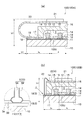
- FIG. 2 is an explanatory view showing an application example to an organic EL device.
- FIG. 2A is a partial sectional view showing an example provided with a conventional conductor connection structure
- FIG. 2B is a partial sectional view showing an example provided with a conductor connection structure according to an embodiment of the present invention. It is.
- the organic EL device 100 (100A, 100B) includes a base 10, a lower electrode 11 formed on the base 10 directly or via another layer, an organic layer 12 stacked on the lower electrode 11, and an organic layer.
- the organic EL element 100U is comprised by the lower electrode 11, the organic layer 12, and the upper electrode 13 on the base
- the upper electrode 13 formed on 12 is provided.
- the organic EL element 100 ⁇ / b> U is formed in a dot matrix in a portion partitioned by the insulating film 14 on the lower electrode 11.
- the lower electrode 11 is formed in a stripe shape, and a stripe-shaped partition wall 15 is formed on the insulating film 14 in a direction crossing the lower electrode 11.
- the organic EL element 100U is disposed in a sealing space S formed by bonding the base body 10 and the sealing base body 16 with the adhesive layer 17. On the outside of the sealing space S on the substrate 10, lead wires 18 connected to the lower electrode 11 or the upper electrode 13 are formed.
- the flexible substrate 20 on which the driving IC 21 is mounted is connected to the lead-out wiring 18 via the ACF 19.
- the substrate region inside the outermost organic EL elements 100U in 10 has become a light emitting region (active area) A L, a region outside the light emitting area A L in the substrate 10 in the frame area A D It has become.
- the frame area AD is inevitably wide in order to secure a pressure-bonding area (connection area) by the ACF 19. Thereby, the effective area
- the flexible substrate 20 is bent and disposed on the back side of the sealing substrate 16, a width W1 required for bending the flexible substrate 20 and a depth W2 for folding and storing the flexible substrate 20 are required. As a result, the space in the electronic device on which the organic EL device 100A is mounted has to be increased.
- the depth W2 is a total value of the width of the driving IC 21, the bending width of the flexible base 20, and the thickness of the base 10 in the thickness direction of the base 10.
- the circuit base 20A on which the driving IC 21 is mounted is disposed on the back surface of the sealing base 16, and the connection between the lead wiring 18 and the wiring on the circuit base 20A is shown in FIG. A wiring connection structure is used.
- the lead wiring 18 corresponds to the wiring 3 in FIG. 1
- the wiring 22 on the circuit base 20A corresponds to the wiring 4 in FIG.
- the lead wiring 18 and the wiring 22 are connected by a bonding wire 23 corresponding to the conductor 5.
- connection part of the bonding wire 23 and the lead-out wiring 18 is shown in the A part enlarged view.
- the bonding wire 23 corresponding to the conductor 5 includes a core portion 5A and a sheath portion 5B.
- the lead wiring 18 includes a conductive portion 3A and a protective portion 3B. The end portion of the bonding wire 23 corresponding to the conductor 5 passes through the protective portion 3B and is electrically connected to the conductive portion 3A.
- connection area in the lead-out wiring 18 can be made relatively small, and the light emission area (active area) A L can be reduced.
- the outer frame area AD can be made smaller than the conventional example shown in FIG.
- the flexible substrate can be eliminated by using the bonding wire 23, the space outside the substrate 10 and the depth W3 can be reduced, and the storage space of the housing for mounting the organic EL device 100B can be reduced. Electronic devices can be made smaller and thinner. Further, by connecting the conductive portion 3A and the bonding wire 23 through the protective portion 3B, the electrical connection can be reliably made to the lead-out wiring 18 covered with the protective portion 3B.
- an organic EL element 100U that is an electronic component connected to the lead-out wiring 18 is disposed on the base body 10 having the lead-out wiring 18 corresponding to the wiring 3, and the organic EL element 100U forms a light emitting portion.
- This light emitting unit may be either for display (display unit) or for illumination (illumination unit).
- display means displaying characters, displaying images, displaying colors, and the like. Illumination refers to illuminating a person or object, or adjusting the brightness of a room.
- the lead-out wiring 18 corresponding to the wiring 3 is provided outside the light emitting part, and is arranged on the outer peripheral part of the base body 10.
- a transparent conductive film for example, a film formed of a material such as ITO, IZO, or IGZO
- the transparent conductive film is patterned by photolithography to form the pattern of the lower electrode 11 and the pattern of the lead wiring 18.
- a first protective part that covers a part or the whole of the lead wiring 18 is formed on the substrate 10.
- a second lead wiring may be formed. That is, the first lead wiring is formed as a lead wiring electrically connected to the lower electrode, and the second lead wiring is formed as a lead wiring electrically connected to the second electrode described later.
- the second lead-out wiring is formed at a position different from the first lead-out wiring and around the light emitting portion (the outer peripheral portion of the base body 10).
- a metal film (aluminum film) is formed on the first protection portion formed on the base 10, and the metal film is formed by photolithography using the first protection portion.
- a second lead wiring is formed by pattern formation.
- a second protective portion for protecting the metal film is formed, and the second protective portion is patterned by photolithography.
- the organic EL element 100B is formed by vapor deposition, coating, sputtering, CVD, or the like. Later, a second protective portion is formed. If necessary, the third protective portion may be formed after the second protective portion is formed.
- a transparent conductive film film such as ITO
- a first protective film a metal film (aluminum film), and a second protective film are formed on the substrate 10 side, and a lead wiring 18 that is sequentially stacked is formed. Is done.
- the transparent conductive film and the first protective film may be patterned by photolithography.
- the metal film and the second protective part are formed so as to cover the first protective part and the substrate 10, and then the metal film and the second protective part are formed by photolithography. The part may be patterned.
- the first lead wire has a transparent conductive film: ITO (about 1.55 ⁇ m), a first protective portion. : An alloy of Ni and Mo (about 0.5 ⁇ m), the second lead wiring, as a first example, a metal film: Al (about 2.3 ⁇ m), a second protective part: an alloy of Mo and Nb, The third protective part is an alloy of Ni and Mo.
- the transparent conductive film ITO (about 1.55 ⁇ m)
- the first protective part an alloy of Mo and Nb (about 0.5 ⁇ m)
- the metal film can be an alloy of Al and Nb (about 3.0 ⁇ m)
- the second protective part can be an alloy of Ni and Nb.
- FIG. 3 is an explanatory view showing an application example to a liquid crystal device.
- the liquid crystal device 200 includes a first base 31, a second base 32, and a sealing member 33.
- the liquid crystal layer 30 is sandwiched between the first base 31 and the second base 32 and the periphery thereof is sealed. Sealed with a member 33.
- the first substrate 31 is a transparent substrate and includes a transparent electrode (not shown) on the liquid crystal layer 30 side, and further includes a color filter, a liquid crystal alignment film, and the like.
- the second substrate 32 is a transparent substrate and includes a transparent electrode (not shown) on the liquid crystal layer 30 side.
- the second base 32 includes a pixel electrode that forms a display pixel and a driving element (TFT element) that drives liquid crystal for each pixel in accordance with an image signal.
- TFT element driving element
- a lead-out wiring 35 is drawn outside the liquid crystal layer 30 in the first base 31 and a connection wiring 34 is patterned.
- One terminal 36B of the control element 36 is connected to the lead-out wiring 35, and the other terminal 36A of the control element 36 is connected to the connection wiring 34.
- an external connection member 38 is mounted on the first base 31 via an adhesive member 37.
- the wiring connection structure shown in FIG. 1 is used as a structure for connecting the connection wiring 34 and the external connection member 38.
- the connection wiring 34 is the wiring 3 in FIG. 1, and the wiring (not shown) on the external connection member 38 corresponds to the wiring 4 in FIG.
- These wires are connected by bonding wires 40 corresponding to the conductors 5. That is, the connection part (A part) of the bonding wire 40 and the connection wiring 34 has a structure as shown in the A part enlarged view shown in FIG.
- the external connection member 38, the bonding wire 40, the control element 36, and the connection wiring 34 can be covered with the sealing material 41.
- connection structure by employing the connection structure by the bonding wire 40, enables narrow dark circles of the connection region of the connection wiring 34, the display region (accession Dib area) A L outside the frame area A D can be reduced.
- the flexible substrate can be eliminated by adopting the bonding wire 40, the storage space of the housing in which the liquid crystal device 200 is mounted can be reduced, and the electronic device can be reduced in size and thickness.
- the conductive portion 3A and the bonding wire 40 through the protective portion 3B in the connection wiring 34, it is possible to reliably make an electrical connection to the connection wiring 34 covered with the protective portion 3B. it can.
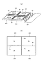
- the example shown in FIG. 4 is an example in which a plurality of light emitting or display devices 300 are combined in a plane to form one panel, and the wiring connection between the plurality of light emitting or display devices 300, 300 and the light emitting or display device.
- the wiring connection structure shown in FIG. 1 is used for the wiring connection between 300 and the external circuit 301.
- 4A shows the connection structure on the back side
- FIG. 4B shows the light emission or display surface.
- the lead-out wiring of one light emission or display device 300 is the wiring 3
- the lead-out wiring of another light emission or display device 300 is the wiring 4.
- a bonding wire 50 that connects between the different light emitting or display devices 300, 300 or between the light emitting or display device 300 and the external circuit 301 corresponds to the conductor 5.
- connection area can be made relatively small, and the frame area outside the display or light emitting area (active area) can be made small. be able to.
- the connection area can be made relatively small, and the frame area outside the display or light emitting area (active area) can be made small. be able to.
- FIG.4 (b) it can make it inconspicuous by narrowing the boundary part Ap as much as possible in the state which combined several display or light emission area
- the plurality of display devices 300 illustrated in FIG. 4 may be electronic devices such as a switch including the display device 300.
- connection structure between the wiring (first wiring) 3 on the first base 1 and the conductor 5 is the same as the wiring (second wiring) 4 on the second base 2 and the conductor 5. You may apply to this connection structure.
- the conductor connection structure according to the embodiment of the present invention is not limited to the application to the light emitting device and the display device as described above, but to various electronic devices including a semiconductor device, a switch having a touch panel, and the like. Applicable.
- the electronic device here is not limited to an electronic device that can be installed or carried by itself, but includes, for example, an electronic device that is installed in the interior of a car or in a house.
Landscapes
- Electroluminescent Light Sources (AREA)
Abstract
Le but de la présente invention est de restreindre la zone de connexion sur un corps de base tel qu'un dispositif émetteur de lumière, un dispositif d'affichage et ainsi de suite, de permettre une trame étroite, et ainsi d'obtenir un équipement électronique plus fin et plus petit. L'invention porte sur une section conductrice (3A) disposée sur un corps de base (1), une section protectrice (3B) pour recouvrir la section conductrice (3A), et un conducteur (5). Le conducteur (5) est connecté à la section conductrice (3A) par la section protectrice (3B) et le conducteur (5) est formé d'un matériau qui est plus dur que l'or.
Priority Applications (1)
| Application Number | Priority Date | Filing Date | Title |
|---|---|---|---|
| PCT/JP2012/065632 WO2013190638A1 (fr) | 2012-06-19 | 2012-06-19 | Structure de connexion de conducteur, équipement électronique |
Applications Claiming Priority (1)
| Application Number | Priority Date | Filing Date | Title |
|---|---|---|---|
| PCT/JP2012/065632 WO2013190638A1 (fr) | 2012-06-19 | 2012-06-19 | Structure de connexion de conducteur, équipement électronique |
Publications (1)
| Publication Number | Publication Date |
|---|---|
| WO2013190638A1 true WO2013190638A1 (fr) | 2013-12-27 |
Family
ID=49768269
Family Applications (1)
| Application Number | Title | Priority Date | Filing Date |
|---|---|---|---|
| PCT/JP2012/065632 Ceased WO2013190638A1 (fr) | 2012-06-19 | 2012-06-19 | Structure de connexion de conducteur, équipement électronique |
Country Status (1)
| Country | Link |
|---|---|
| WO (1) | WO2013190638A1 (fr) |
Cited By (5)
| Publication number | Priority date | Publication date | Assignee | Title |
|---|---|---|---|---|
| JP2014090036A (ja) * | 2012-10-29 | 2014-05-15 | Kaneka Corp | 有機el装置 |
| WO2014162802A1 (fr) * | 2013-04-01 | 2014-10-09 | パイオニア株式会社 | Dispositif optique |
| WO2015125309A1 (fr) * | 2014-02-24 | 2015-08-27 | パイオニア株式会社 | Dispositif électroluminescent |
| WO2015141088A1 (fr) * | 2014-03-20 | 2015-09-24 | パイオニア株式会社 | Dispositif émetteur de lumière |
| CN114175222A (zh) * | 2019-07-25 | 2022-03-11 | 日立能源瑞士股份公司 | 功率半导体模块 |
Citations (6)
| Publication number | Priority date | Publication date | Assignee | Title |
|---|---|---|---|---|
| JPS63148646A (ja) * | 1986-12-12 | 1988-06-21 | Toshiba Corp | 半導体装置 |
| JPH03116941A (ja) * | 1989-09-29 | 1991-05-17 | Fujitsu Ltd | 半導体装置の製造方法 |
| JPH0494752U (fr) * | 1990-12-29 | 1992-08-17 | ||
| JPH06333977A (ja) * | 1993-05-25 | 1994-12-02 | Nippon Steel Corp | 半導体装置及びその製造方法 |
| JP2003229517A (ja) * | 2002-01-31 | 2003-08-15 | Fujitsu Hitachi Plasma Display Ltd | 半導体チップ実装基板及びフラットディスプレイ |
| JP2012079944A (ja) * | 2010-10-01 | 2012-04-19 | Nippon Steel Materials Co Ltd | 複層銅ボンディングワイヤの接合構造 |
-
2012
- 2012-06-19 WO PCT/JP2012/065632 patent/WO2013190638A1/fr not_active Ceased
Patent Citations (6)
| Publication number | Priority date | Publication date | Assignee | Title |
|---|---|---|---|---|
| JPS63148646A (ja) * | 1986-12-12 | 1988-06-21 | Toshiba Corp | 半導体装置 |
| JPH03116941A (ja) * | 1989-09-29 | 1991-05-17 | Fujitsu Ltd | 半導体装置の製造方法 |
| JPH0494752U (fr) * | 1990-12-29 | 1992-08-17 | ||
| JPH06333977A (ja) * | 1993-05-25 | 1994-12-02 | Nippon Steel Corp | 半導体装置及びその製造方法 |
| JP2003229517A (ja) * | 2002-01-31 | 2003-08-15 | Fujitsu Hitachi Plasma Display Ltd | 半導体チップ実装基板及びフラットディスプレイ |
| JP2012079944A (ja) * | 2010-10-01 | 2012-04-19 | Nippon Steel Materials Co Ltd | 複層銅ボンディングワイヤの接合構造 |
Cited By (7)
| Publication number | Priority date | Publication date | Assignee | Title |
|---|---|---|---|---|
| JP2014090036A (ja) * | 2012-10-29 | 2014-05-15 | Kaneka Corp | 有機el装置 |
| WO2014162802A1 (fr) * | 2013-04-01 | 2014-10-09 | パイオニア株式会社 | Dispositif optique |
| WO2015125309A1 (fr) * | 2014-02-24 | 2015-08-27 | パイオニア株式会社 | Dispositif électroluminescent |
| JPWO2015125309A1 (ja) * | 2014-02-24 | 2017-03-30 | パイオニア株式会社 | 発光装置 |
| WO2015141088A1 (fr) * | 2014-03-20 | 2015-09-24 | パイオニア株式会社 | Dispositif émetteur de lumière |
| CN114175222A (zh) * | 2019-07-25 | 2022-03-11 | 日立能源瑞士股份公司 | 功率半导体模块 |
| CN114175222B (zh) * | 2019-07-25 | 2025-05-23 | 日立能源有限公司 | 功率半导体模块 |
Similar Documents
| Publication | Publication Date | Title |
|---|---|---|
| CN107706156B (zh) | 一种柔性显示基板及其制备方法、柔性显示装置 | |
| CN108228002B (zh) | 触控面板及应用其的触控显示装置 | |
| JP2021170118A (ja) | 電子機器 | |
| CN108206202B (zh) | 柔性显示装置 | |
| CN113555375B (zh) | 显示设备 | |
| US20140138141A1 (en) | Peripheral circuit structure | |
| US10288959B2 (en) | Display device comprising first and second oxide conductive films that cover a terminal wire | |
| US20160274701A1 (en) | Touch Window | |
| KR20200110491A (ko) | 표시 장치 | |
| KR102053427B1 (ko) | 터치 센서 및 이를 포함하는 화상 표시 장치 | |
| CN113366419B (zh) | 触摸传感器以及包括该触摸传感器的窗口层叠体和图像显示装置 | |
| JP2018054678A (ja) | 表示装置及びその製造方法 | |
| JP4815868B2 (ja) | 表示装置 | |
| CN112951880B (zh) | 包括连接结构的有机发光显示装置 | |
| KR102819881B1 (ko) | 터치 센서 및 이를 포함하는 화상 표시 장치 | |
| JP5591411B1 (ja) | 有機el装置 | |
| US10304855B2 (en) | Display panel, touch display device and wire structure | |
| JP2008294290A (ja) | 基板及び電気光学装置並びに電子機器 | |
| WO2011016286A1 (fr) | Substrat de matrice active, panneau et dispositif d'affichage à cristaux liquides, et procédé de fabrication d'un substrat de matrice active | |
| JP2015015246A (ja) | 有機el装置 | |
| CN112955813A (zh) | 绑定背板及其制作方法、背光模组及显示装置 | |
| EP4300470A1 (fr) | Substrat d'attaque et son procédé de préparation, et appareil électroluminescent | |
| CN112864658B (zh) | 包括连接器的显示设备 | |
| JP2019045718A (ja) | 表示パネルおよびタイリング表示装置 | |
| JP2006072286A (ja) | ディスプレイ装置の導線端子構造 |
Legal Events
| Date | Code | Title | Description |
|---|---|---|---|
| 121 | Ep: the epo has been informed by wipo that ep was designated in this application |
Ref document number: 12879520 Country of ref document: EP Kind code of ref document: A1 |
|
| NENP | Non-entry into the national phase |
Ref country code: DE |
|
| 122 | Ep: pct application non-entry in european phase |
Ref document number: 12879520 Country of ref document: EP Kind code of ref document: A1 |
|
| NENP | Non-entry into the national phase |
Ref country code: JP |